EP1146393A2 - Verfahren zur Herstellung von Masken für die Fertigung von Halbleiterstrukturen - Google Patents
Verfahren zur Herstellung von Masken für die Fertigung von Halbleiterstrukturen Download PDFInfo
- Publication number
- EP1146393A2 EP1146393A2 EP01107628A EP01107628A EP1146393A2 EP 1146393 A2 EP1146393 A2 EP 1146393A2 EP 01107628 A EP01107628 A EP 01107628A EP 01107628 A EP01107628 A EP 01107628A EP 1146393 A2 EP1146393 A2 EP 1146393A2
- Authority
- EP
- European Patent Office
- Prior art keywords
- layout data
- mask
- layout
- edges
- geometric
- Prior art date
- Legal status (The legal status is an assumption and is not a legal conclusion. Google has not performed a legal analysis and makes no representation as to the accuracy of the status listed.)
- Granted
Links
Images


Classifications
-
- G—PHYSICS
- G03—PHOTOGRAPHY; CINEMATOGRAPHY; ANALOGOUS TECHNIQUES USING WAVES OTHER THAN OPTICAL WAVES; ELECTROGRAPHY; HOLOGRAPHY
- G03F—PHOTOMECHANICAL PRODUCTION OF TEXTURED OR PATTERNED SURFACES, e.g. FOR PRINTING, FOR PROCESSING OF SEMICONDUCTOR DEVICES; MATERIALS THEREFOR; ORIGINALS THEREFOR; APPARATUS SPECIALLY ADAPTED THEREFOR
- G03F1/00—Originals for photomechanical production of textured or patterned surfaces, e.g., masks, photo-masks, reticles; Mask blanks or pellicles therefor; Containers specially adapted therefor; Preparation thereof
- G03F1/68—Preparation processes not covered by groups G03F1/20 - G03F1/50
- G03F1/70—Adapting basic layout or design of masks to lithographic process requirements, e.g., second iteration correction of mask patterns for imaging
Definitions
- the present invention relates to a method for manufacturing of masks for the production of semiconductor structures, in which the production of a mask based on layout data the information for defining a mask layout included, which has individual geometric structural elements.
- auxiliary structures are used, for example, for planarization. They are not electrically effective and do allow certain geometric freedom in the design of the corresponding Mask structure. Examples of technological advantages which can be achieved by modifying mask structures, are improvement of imaging properties, process window enlargement (Process window as a general term for allowed Scattering of process parameters), improvement of Planarization properties, increase in yield or more robust design.
- the process for the production of masks is carried out a mask usually based on generated layout data, contain the information for defining a mask layout.
- the mask layout has individual geometric ones Structure elements that represent the mask structures. Often when generating the layout data is the generation Multiple mask levels necessary to complete the manufacturing process to optimize.
- the object of the present invention is a method for the production of masks for the production of semiconductor structures specify where a modification of generated Layout data of a mask to be produced to eliminate Generation errors occur, so that the manufacturability of the Mask is guaranteed, and a relatively quick Modification of the layout data and its technology-dependent Optimization allowed.
- the Structural elements and their design requirements through so-called characterize attributes describing the situation to let. For example, isolated lines through the attribute from that at a certain distance no neighboring Structures are. Structures for certain mask levels Planarization properties are improved by the attribute of a sufficiently large structure on the one to be planarized Mask level described. Leave such attributes with a software for physical verification (e.g. Find and classify "Vampires"). This classified Attributes are also called “markers”. These markers are now used to lay out the data to modify depending on the situation.
- the other layout data that the information included to set the correction figures, with consideration generated to the mask requirements.
- the other layout data are modified, for example, by modifying the layout data of the respective fault locations.
- layout data to be produced Creates a mask for one or more mask layers, so the method can be beneficial for each of the mask planes be performed.
- the method according to the invention allows the generation the layout data of a mask to be produced Errors completely, fully automatically and according to technological to fix predefined optimization criteria.
- the process can be implemented relatively easily in existing standard design processes (Design flows) can be integrated. It can have different technological constraints for the Generation of the layout data can be specified so that a optimized solution can be found according to these boundary conditions can.
- the method can be designed so that Manual rework can be omitted, making the process is accelerated overall.
- the generation errors can be corrected by adding correction figures at the corresponding fault locations or by cutting back of the structural elements at the fault locations become.
- the layout data is sent to the respective Fault locations with the other layout data to be determined of the correction figures additively linked.
- the layout data of the respective fault locations with the others Layout data subtractively linked (subtractive correction figures).
- the method is used to manufacture masks for Manufacture of semiconductor structures of an integrated circuit, which are electrically effective, is when performing the procedure to ensure that the so-called Connectivity relationships between the structural elements of the Mask not changed when modifying layout data become.
- the associated geometrical configurations Store correction figures in a data library and to reuse the results.
- the Layout data of a mask to be produced and the respective associated one further layout data for defining associated correction figures stored in a data library are identical to each other.
- any errors in the modification of the layout data arise (so-called secondary errors) eliminated iteratively.
- secondary errors To are the steps of checking the layout data, the Localization of the fault locations, generation of further layout data and linking the layout data with the others Layout data carried out in succession until no design requirements get hurt more. Existing secondary errors are repeated application of the test and modification steps eliminated.
- the correction figures can be parameterized.
- the further layout data is generated such that the edges of the correction figures are parameterized.
- the context of the parameterized edges becomes inequalities for the edges of the correction figures that the describe the potential positions of the edges. It becomes an optimization criterion regarding the geometric requirements of the correction figures.
- To determine the respective Laying the edges becomes a mathematical optimization process applied so that in each case the inequalities and the optimization criterion are met. Thereby are the correction figures due to the specific positions of the edges fixed.
- the correction figures can be context-dependent and according to the optimization criterion exactly in the required form. So there are no secondary errors.
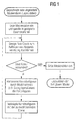
- layout data is first of all to produce mask in the form of drawn or derived Mask data generated. These are used for further processing read into a processing device and into suitable Data structures converted.
- design rule check carried out, for example, using verification software to find distance violations.
- Violation of design requirements will be the appropriate Fault locations in the mask layout are localized based on the layout data.
- layout data to define Correction figures generated. These can be, for example, by Modifications such as Sizing operations of the error figures be constructed.
- FIG. 2a A configuration of a mask layout 1 is shown in FIG. 2a Structural elements 2 shown that a distance violation have in the form of the fault location or the fault figure 10.
- the error figure 10 is modified, so that the correction figure 11 is generated.
- Figure 2c shows with the existing structural elements connected.
- the error figure 12 is the same Way as described above by overlaying the Correction figure 13 modified ( Figure 2d).
- Figure 2e shown a new configuration is created after this second iteration step with a new distance violation in the form of the error figure 14.
- By overlaying another The producible configuration is created according to the corrective figure without distance violations after three iteration steps, as shown in Figure 2f.
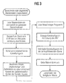
- the layout data are similar to the example in FIG generated and read.
- parameterized correction figures generated. These are initially generated in such a way that the edges of the correction figures are parameterized. Out the geometric context of the parameterized edges the linear inequalities for the edges of the correction figures set up, which describe potential positions of the edges.
- an optimization criterion or an objective function regarding the geometric requirements of the correction figures set up With the help of a mathematical optimization process, e.g. a so-called mixed integer programming process, become layers of the edges of the correction figures which determines the inequalities and meet the optimization criterion. The correction figures are thus determined by the specific positions of the edges.
- MIP mixed integer programming method
- the optimization criterion is, for example around a linear polynomial in the possible for the description Edge layers used variables. For example, there is Optimization criterion that the edges of the correction figures, based on their starting position, shifted as little as possible become. Another optimization criterion is, for example assumes that the surfaces of the correction figures are as possible are small. In this way, different Create variants of an optimization criterion so that different ones geometric arrangements of the correction figures can be optimized.
- FIG. 4a shows a configuration of a mask layout 1 with Structural elements 2 with distance violations in the form of the error figures 20 and 21.
- Correction figures 22 generated with parameterized edges. there is the position of each of the edges in a certain area freely selectable, the conditions between the edges are given by the inequalities established.
- Figure 4c are exemplary relationships between the edges for determination the inequalities and the objective function.
- the individual correction figures are determined in such a way that no more distance violation occurs, here also secondary Width injuries are avoided.
- Figure 4d shown a producible configuration without distance violations. Since the respective correction figures through targeted parameterization can be generated under certain circumstances a higher Accuracy compared to the iterative process become.
Landscapes
- Physics & Mathematics (AREA)
- General Physics & Mathematics (AREA)
- Preparing Plates And Mask In Photomechanical Process (AREA)
- Design And Manufacture Of Integrated Circuits (AREA)
Abstract
Description
- es werden Layoutdaten eines herzustellenden Maskenlayouts erzeugt,
- es werden geometrische Design-Anforderungen für einzelne Strukturelemente und deren Anordnung festgelegt,
- es werden die Layoutdaten dahingehend überprüft, ob die geometrischen Design-Anforderungen für die einzelnen Strukturelemente und deren Anordnung erfüllt sind,
- im Falle der Verletzung von Design-Anforderungen werden die entsprechenden Fehlerorte im Maskenlayout anhand der Layoutdaten lokalisiert,
- es werden weitere Layoutdaten erzeugt, die Information zum Festlegen von Korrekturfiguren zur Korrektur der jeweiligen Fehlerorte enthalten,
- es werden die Layoutdaten mit den weiteren Layoutdaten verknüpft, so daß die Layoutdaten modifiziert werden.
- Figur 1
- ein Flußdiagramm einer Ausführungsform des erfindungsgemäßen Verfahrens,
- Figur 2
- ein geometrisches Beispiel zur Durchführung des Verfahrens gemäß Figur 1,
- Figur 3
- ein Flußdiagramm einer weiteren Ausführungsform des erfindungsgemäßen Verfahrens,
- Figur 4
- ein geometrisches Beispiel zur Durchführung des Verfahrens gemäß Figur 3.
Claims (10)
- Verfahren zur Herstellung von Masken für die Fertigung von Halbleiterstrukturen, bei dem die Herstellung einer Maske anhand von Layoutdaten erfolgt, die Information zum Festlegen eines Maskenlayouts (1) enthalten, das einzelne geometrische Strukturelemente (2) aufweist,
mit den Merkmalen:es werden Layoutdaten eines herzustellenden Maskenlayouts (1) erzeugt,es werden geometrische Design-Anforderungen für einzelne Strukturelemente (2) und deren Anordnung festgelegt,es werden die Layoutdaten dahingehend überprüft, ob die geometrischen Design-Anforderungen für die einzelnen Strukturelemente (2) und deren Anordnung erfüllt sind,im Falle der Verletzung von Design-Anforderungen werden die entsprechenden Fehlerorte (10, 20) im Maskenlayout (1) anhand der Layoutdaten lokalisiert,es werden weitere Layoutdaten erzeugt, die Information zum Festlegen von Korrekturfiguren (11, 22) zur Korrektur der jeweiligen Fehlerorte (10, 20) enthalten,es werden die Layoutdaten mit den weiteren Layoutdaten verknüpft, so daß die Layoutdaten modifiziert werden. - Verfahren nach Anspruch 1,
dadurch gekennzeichnet, daß
die weiteren Layoutdaten durch Modifikation der Layoutdaten der jeweiligen Fehlerorte (10, 20) erzeugt werden. - Verfahren nach einem der Ansprüche 1 oder 2,
dadurch gekennzeichnet, daß
Layoutdaten für eine oder mehrere Maskenebenen erzeugt werden und das Verfahren für jede der Maskenebenen durchgeführt wird. - Verfahren nach einem der Ansprüche 1 bis 3,
dadurch gekennzeichnet, daß
die Schritte der Überprüfung der Layoutdaten, der Lokalisierung der Fehlerorte (10, 20), der Erzeugung der weiteren Layoutdaten und der Verknüpfung der Layoutdaten mit den weiteren Layoutdaten solange nacheinander durchgeführt werden, bis keine Design-Anforderungen mehr verletzt werden. - Verfahren nach einem der Ansprüche 1 bis 3,
dadurch gekennzeichnet, daßdie weiteren Layoutdaten derart erzeugt werden, daß die Kanten der Korrekturfiguren (22) parametrisiert sind,aus dem geometrischen Kontext der parametrisierten Kanten Ungleichungen für die Kanten der Korrekturfiguren (22) aufgestellt werden, die potentielle Lagen der Kanten beschreiben,ein Optimierungskriterium bezüglich den geometrischen Anforderungen der Korrekturfiguren (22) aufgestellt wird,ein mathematisches Optimierungsverfahren angewandt wird zur Bestimmung der jeweiligen Lagen der Kanten, so daß jeweils die aufgestellten Ungleichungen und das Optimierungskriterium erfüllt sind,die Korrekturfiguren (22) durch die bestimmten Lagen der Kanten festgelegt sind. - Verfahren nach Anspruch 5,
dadurch gekennzeichnet, daß
als mathematisches Optimierungsverfahren ein Mixed-Integer-Programming-Verfahren verwendet wird. - Verfahren nach einem der Ansprüche 1 bis 6,
dadurch gekennzeichnet, daß
die Layoutdaten mit den weiteren Layoutdaten additiv oder subtraktiv verknüpft werden. - Verfahren nach einem der Ansprüche 1 bis 7,
dadurch gekennzeichnet, daß
die Layoutdaten und die jeweils zugehörigen weiteren Layoutdaten in einer Datenbibliothek gespeichert werden. - Verfahren nach einem der Ansprüche 1 bis 8,
dadurch gekennzeichnet, daß
die Layoutdaten eine hierarchische Struktur aufweisen und die Layoutdaten anhand des Verfahrens nacheinander gemäß ihrer hierarchischen Struktur unter Berücksichtigung des jeweiligen geometrischen Kontexts modifiziert werden. - Verfahren nach einem der Ansprüche 1 bis 9,
dadurch gekennzeichnet, daß
die Maske zur Fertigung von Hilfsstrukturen einer integrierten Schaltung dient, die in der integrierten Schaltung elektrisch nicht wirksam sind.
Applications Claiming Priority (2)
| Application Number | Priority Date | Filing Date | Title |
|---|---|---|---|
| DE10017767A DE10017767A1 (de) | 2000-04-10 | 2000-04-10 | Verfahren zur Herstellung von Masken für die Fertigung von Halbleiterstrukturen |
| DE10017767 | 2000-04-10 |
Publications (3)
| Publication Number | Publication Date |
|---|---|
| EP1146393A2 true EP1146393A2 (de) | 2001-10-17 |
| EP1146393A3 EP1146393A3 (de) | 2005-07-20 |
| EP1146393B1 EP1146393B1 (de) | 2016-11-02 |
Family
ID=7638222
Family Applications (1)
| Application Number | Title | Priority Date | Filing Date |
|---|---|---|---|
| EP01107628.8A Expired - Lifetime EP1146393B1 (de) | 2000-04-10 | 2001-03-27 | Verfahren zur Herstellung von Masken für die Fertigung von Halbleiterstrukturen |
Country Status (4)
| Country | Link |
|---|---|
| US (1) | US6493865B2 (de) |
| EP (1) | EP1146393B1 (de) |
| DE (1) | DE10017767A1 (de) |
| TW (1) | TW565750B (de) |
Cited By (1)
| Publication number | Priority date | Publication date | Assignee | Title |
|---|---|---|---|---|
| US10216890B2 (en) | 2004-04-21 | 2019-02-26 | Iym Technologies Llc | Integrated circuits having in-situ constraints |
Families Citing this family (7)
| Publication number | Priority date | Publication date | Assignee | Title |
|---|---|---|---|---|
| US6899981B1 (en) * | 2001-11-21 | 2005-05-31 | Dupont Photomasks, Inc. | Photomask and method for detecting violations in a mask pattern file using a manufacturing rule |
| DE10206658B4 (de) * | 2002-02-15 | 2011-11-17 | Qimonda Ag | Verfahren zum Überprüfen einer integrierten elektrischen Schaltung |
| US7093228B2 (en) * | 2002-12-20 | 2006-08-15 | Lsi Logic Corporation | Method and system for classifying an integrated circuit for optical proximity correction |
| US6904587B2 (en) * | 2002-12-20 | 2005-06-07 | Synopsys, Inc. | Incremental lithography mask layout design and verification |
| KR100576831B1 (ko) * | 2004-11-02 | 2006-05-10 | 삼성전자주식회사 | 데이터 변환 장비의 데이터 검증 방법 |
| US10282221B2 (en) | 2011-12-09 | 2019-05-07 | International Business Machines Corporation | Controlling usage of virtual disks before their attachment to virtual machines |
| JP6782769B2 (ja) | 2015-09-28 | 2020-11-11 | エーエスエムエル ネザーランズ ビー.ブイ. | 2次元又は3次元の形状の階層的表現 |
Family Cites Families (13)
| Publication number | Priority date | Publication date | Assignee | Title |
|---|---|---|---|---|
| JP2509755B2 (ja) * | 1990-11-22 | 1996-06-26 | 株式会社東芝 | 半導体集積回路製造方法 |
| US5535134A (en) * | 1994-06-03 | 1996-07-09 | International Business Machines Corporation | Object placement aid |
| KR960002536A (de) | 1994-06-29 | 1996-01-26 | ||
| JPH08297692A (ja) | 1994-09-16 | 1996-11-12 | Mitsubishi Electric Corp | 光近接補正装置及び方法並びにパタン形成方法 |
| JP2996127B2 (ja) | 1995-02-17 | 1999-12-27 | 日本電気株式会社 | パターン形成方法 |
| US5801954A (en) * | 1996-04-24 | 1998-09-01 | Micron Technology, Inc. | Process for designing and checking a mask layout |
| JP3373748B2 (ja) | 1997-02-07 | 2003-02-04 | 株式会社東芝 | 半導体装置の製造方法 |
| JP3011120B2 (ja) * | 1997-02-13 | 2000-02-21 | 日本電気株式会社 | レイアウト情報生成装置及びレイアウト情報生成方法 |
| JP3367378B2 (ja) * | 1997-04-25 | 2003-01-14 | 豊田合成株式会社 | エアバッグモジュール |
| DE19818440C2 (de) | 1998-04-24 | 2002-10-24 | Pdf Solutions Gmbh | Verfahren zur Erzeugung von Daten für die Herstellung einer durch Entwurfsdaten definierten Struktur |
| TW376465B (en) | 1998-09-03 | 1999-12-11 | United Microelectronics Corp | Method for automatically generating assist phase shifting mask (PSM) |
| TW372283B (en) | 1998-09-05 | 1999-10-21 | United Microelectronics Corp | Method for automatically generating annular phase shifting mask |
| JP3751762B2 (ja) * | 1998-12-08 | 2006-03-01 | 株式会社東芝 | 半導体装置の製造方法および原板 |
-
2000
- 2000-04-10 DE DE10017767A patent/DE10017767A1/de not_active Ceased
-
2001
- 2001-03-27 EP EP01107628.8A patent/EP1146393B1/de not_active Expired - Lifetime
- 2001-04-09 TW TW090108422A patent/TW565750B/zh not_active IP Right Cessation
- 2001-04-10 US US09/829,870 patent/US6493865B2/en not_active Expired - Lifetime
Cited By (3)
| Publication number | Priority date | Publication date | Assignee | Title |
|---|---|---|---|---|
| US10216890B2 (en) | 2004-04-21 | 2019-02-26 | Iym Technologies Llc | Integrated circuits having in-situ constraints |
| US10846454B2 (en) | 2004-04-21 | 2020-11-24 | Iym Technologies Llc | Integrated circuits having in-situ constraints |
| US10860773B2 (en) | 2004-04-21 | 2020-12-08 | Iym Technologies Llc | Integrated circuits having in-situ constraints |
Also Published As
| Publication number | Publication date |
|---|---|
| DE10017767A1 (de) | 2001-10-18 |
| TW565750B (en) | 2003-12-11 |
| EP1146393A3 (de) | 2005-07-20 |
| US20020112222A1 (en) | 2002-08-15 |
| US6493865B2 (en) | 2002-12-10 |
| EP1146393B1 (de) | 2016-11-02 |
Similar Documents
| Publication | Publication Date | Title |
|---|---|---|
| DE60116769T2 (de) | Verfahren und system zur hierarchischen metallenden-, einschliessungs- und belichtungsprüfung | |
| DE69521507T2 (de) | System und verfahren zur auf einem modell basierender prüfung von lokalen entwurfsregeln | |
| DE69813892T2 (de) | Polygon darstellung im layout eines integrierten schaltkreises | |
| DE102015200694A1 (de) | Verfahren, computersystem und computerlesbares speichermedium zum erzeugen eines layouts eines integrierten schaltkreises | |
| DE10025583A1 (de) | Verfahren zur Optimierung integrierter Schaltungen, Vorrichtung zum Entwurf von Halbleitern und Programmobjekt zum Entwerfen integrierter Schaltungen | |
| DE68929052T2 (de) | Verfahren zur Knotenpositionierung in einem graphen-basierenden Diagramm | |
| DE3900750A1 (de) | Wissensbasis - verfahren - vorrichtung zum entwerfen integrierter schaltungen mittels funktionaler spezifikationen | |
| DE112013005820T5 (de) | Graphische Benutzerschnittstelle für ein Werkzeug zur Lageplanerstellung bei der Entwurfsautomatisierung elektronischer Systeme | |
| DE102019116952B4 (de) | Integrierte-schaltkreis-struktur, layout-schaubild-verfahren und system | |
| DE3854755T2 (de) | Prozess zur Herstellung von Halbleitern, bei dem die Bildverzeichnung zwischen dem Muster auf der Halbleiteroberfläche und der dieses erzeugenden Maske kompensiert wird. | |
| DE102019123621A1 (de) | Routungsressourcenverbesserndes verfahren zum generieren von layout-diagrammen, und system dafür | |
| EP1146393B1 (de) | Verfahren zur Herstellung von Masken für die Fertigung von Halbleiterstrukturen | |
| DE10205330A1 (de) | Verfahren zur Korrektur optischer Nachbarschaftseffekte | |
| DE10138142B4 (de) | Verfahren zur Analyse einer integrierten elektrischen Schaltung | |
| DE3337300A1 (de) | Verfahren zum herstellen integrierter halbleiterschaltkreise | |
| EP1543452B1 (de) | Verfahren zum bestimmen der anordnung von kontaktflächen auf der aktiven oberseite eines halbleiterchips | |
| DE102021119949A1 (de) | Geometrische maskenregelkontrolle mit günstigen und ungünstigen zonen | |
| DE10063099A1 (de) | Verfahren zum überprüfen von über einer Photomaske ausgebildeten Belichtungsmustern | |
| DE10206658B4 (de) | Verfahren zum Überprüfen einer integrierten elektrischen Schaltung | |
| DE102005003001A1 (de) | Verfahren zur Korrektur des optischen Proximity-Effektes | |
| DE10149021B4 (de) | Datenverarbeitungssystem zum Entwurf eines Layouts einer integrierten elektronischen Schaltung aus einer Vielzahl von elektronischen Bauelementen | |
| DE10304674A1 (de) | Verfahren zum Belichten eines Substrates mit einem den optischen Proximity-Effekt ausgleichenden Strukturmuster | |
| DE10245621A1 (de) | Verfahren zur Übergabe einer Meßposition eines auf einer Maske zu bildenden Strukturelementes | |
| DE102005039394B4 (de) | Verfahren zum Suchen potentieller Fehler eines Layouts einer integrierten Schaltung | |
| DE102017104049B4 (de) | Verfahren und vorrichtung zum überprüfen der zuverlässigkeit eines chips |
Legal Events
| Date | Code | Title | Description |
|---|---|---|---|
| PUAI | Public reference made under article 153(3) epc to a published international application that has entered the european phase |
Free format text: ORIGINAL CODE: 0009012 |
|
| AK | Designated contracting states |
Kind code of ref document: A2 Designated state(s): AT BE CH CY DE DK ES FI FR GB GR IE IT LI LU MC NL PT SE TR |
|
| AX | Request for extension of the european patent |
Free format text: AL;LT;LV;MK;RO;SI |
|
| PUAL | Search report despatched |
Free format text: ORIGINAL CODE: 0009013 |
|
| AK | Designated contracting states |
Kind code of ref document: A3 Designated state(s): AT BE CH CY DE DK ES FI FR GB GR IE IT LI LU MC NL PT SE TR |
|
| AX | Request for extension of the european patent |
Extension state: AL LT LV MK RO SI |
|
| RIC1 | Information provided on ipc code assigned before grant |
Ipc: 7G 06F 17/50 B Ipc: 7G 03F 1/00 B Ipc: 7G 03F 1/14 A |
|
| 17P | Request for examination filed |
Effective date: 20060120 |
|
| AKX | Designation fees paid |
Designated state(s): DE FR GB IE IT NL |
|
| 17Q | First examination report despatched |
Effective date: 20060622 |
|
| RAP1 | Party data changed (applicant data changed or rights of an application transferred) |
Owner name: INFINEON TECHNOLOGIES AG |
|
| RAP1 | Party data changed (applicant data changed or rights of an application transferred) |
Owner name: QIMONDA AG |
|
| RAP1 | Party data changed (applicant data changed or rights of an application transferred) |
Owner name: INFINEON TECHNOLOGIES AG |
|
| RAP1 | Party data changed (applicant data changed or rights of an application transferred) |
Owner name: POLARIS INNOVATIONS LIMITED |
|
| REG | Reference to a national code |
Ref country code: DE Ref legal event code: R079 Ref document number: 50116591 Country of ref document: DE Free format text: PREVIOUS MAIN CLASS: G03F0001140000 Ipc: G03F0001000000 |
|
| GRAP | Despatch of communication of intention to grant a patent |
Free format text: ORIGINAL CODE: EPIDOSNIGR1 |
|
| RIC1 | Information provided on ipc code assigned before grant |
Ipc: G03F 1/70 20120101ALI20160419BHEP Ipc: G03F 1/00 20120101AFI20160419BHEP |
|
| INTG | Intention to grant announced |
Effective date: 20160511 |
|
| GRAS | Grant fee paid |
Free format text: ORIGINAL CODE: EPIDOSNIGR3 |
|
| GRAA | (expected) grant |
Free format text: ORIGINAL CODE: 0009210 |
|
| AK | Designated contracting states |
Kind code of ref document: B1 Designated state(s): DE FR GB IE IT NL |
|
| REG | Reference to a national code |
Ref country code: GB Ref legal event code: FG4D Free format text: NOT ENGLISH |
|
| REG | Reference to a national code |
Ref country code: IE Ref legal event code: FG4D Free format text: LANGUAGE OF EP DOCUMENT: GERMAN |
|
| REG | Reference to a national code |
Ref country code: DE Ref legal event code: R096 Ref document number: 50116591 Country of ref document: DE |
|
| REG | Reference to a national code |
Ref country code: FR Ref legal event code: PLFP Year of fee payment: 17 |
|
| REG | Reference to a national code |
Ref country code: NL Ref legal event code: MP Effective date: 20161102 |
|
| PG25 | Lapsed in a contracting state [announced via postgrant information from national office to epo] |
Ref country code: NL Free format text: LAPSE BECAUSE OF FAILURE TO SUBMIT A TRANSLATION OF THE DESCRIPTION OR TO PAY THE FEE WITHIN THE PRESCRIBED TIME-LIMIT Effective date: 20161102 |
|
| PGFP | Annual fee paid to national office [announced via postgrant information from national office to epo] |
Ref country code: FR Payment date: 20170213 Year of fee payment: 17 Ref country code: DE Payment date: 20170321 Year of fee payment: 17 |
|
| PGFP | Annual fee paid to national office [announced via postgrant information from national office to epo] |
Ref country code: GB Payment date: 20170322 Year of fee payment: 17 |
|
| REG | Reference to a national code |
Ref country code: DE Ref legal event code: R097 Ref document number: 50116591 Country of ref document: DE |
|
| PG25 | Lapsed in a contracting state [announced via postgrant information from national office to epo] |
Ref country code: IT Free format text: LAPSE BECAUSE OF FAILURE TO SUBMIT A TRANSLATION OF THE DESCRIPTION OR TO PAY THE FEE WITHIN THE PRESCRIBED TIME-LIMIT Effective date: 20161102 |
|
| PLBE | No opposition filed within time limit |
Free format text: ORIGINAL CODE: 0009261 |
|
| STAA | Information on the status of an ep patent application or granted ep patent |
Free format text: STATUS: NO OPPOSITION FILED WITHIN TIME LIMIT |
|
| 26N | No opposition filed |
Effective date: 20170803 |
|
| REG | Reference to a national code |
Ref country code: IE Ref legal event code: MM4A |
|
| PG25 | Lapsed in a contracting state [announced via postgrant information from national office to epo] |
Ref country code: IE Free format text: LAPSE BECAUSE OF NON-PAYMENT OF DUE FEES Effective date: 20170327 |
|
| REG | Reference to a national code |
Ref country code: DE Ref legal event code: R119 Ref document number: 50116591 Country of ref document: DE |
|
| GBPC | Gb: european patent ceased through non-payment of renewal fee |
Effective date: 20180327 |
|
| PG25 | Lapsed in a contracting state [announced via postgrant information from national office to epo] |
Ref country code: DE Free format text: LAPSE BECAUSE OF NON-PAYMENT OF DUE FEES Effective date: 20181002 |
|
| PG25 | Lapsed in a contracting state [announced via postgrant information from national office to epo] |
Ref country code: GB Free format text: LAPSE BECAUSE OF NON-PAYMENT OF DUE FEES Effective date: 20180327 |
|
| PG25 | Lapsed in a contracting state [announced via postgrant information from national office to epo] |
Ref country code: FR Free format text: LAPSE BECAUSE OF NON-PAYMENT OF DUE FEES Effective date: 20180331 |