EP1143508A2 - Vorrichtung zum Verpacken von elektronischen Bauteilen - Google Patents
Vorrichtung zum Verpacken von elektronischen Bauteilen Download PDFInfo
- Publication number
- EP1143508A2 EP1143508A2 EP01106481A EP01106481A EP1143508A2 EP 1143508 A2 EP1143508 A2 EP 1143508A2 EP 01106481 A EP01106481 A EP 01106481A EP 01106481 A EP01106481 A EP 01106481A EP 1143508 A2 EP1143508 A2 EP 1143508A2
- Authority
- EP
- European Patent Office
- Prior art keywords
- plastic
- mounting frame
- intermediate carrier
- semiconductor chips
- semiconductor chip
- Prior art date
- Legal status (The legal status is an assumption and is not a legal conclusion. Google has not performed a legal analysis and makes no representation as to the accuracy of the status listed.)
- Withdrawn
Links
Images



Classifications
-
- H—ELECTRICITY
- H10—SEMICONDUCTOR DEVICES; ELECTRIC SOLID-STATE DEVICES NOT OTHERWISE PROVIDED FOR
- H10W—GENERIC PACKAGES, INTERCONNECTIONS, CONNECTORS OR OTHER CONSTRUCTIONAL DETAILS OF DEVICES COVERED BY CLASS H10
- H10W72/00—Interconnections or connectors in packages
- H10W72/01—Manufacture or treatment
- H10W72/0198—Manufacture or treatment batch processes
-
- H—ELECTRICITY
- H10—SEMICONDUCTOR DEVICES; ELECTRIC SOLID-STATE DEVICES NOT OTHERWISE PROVIDED FOR
- H10W—GENERIC PACKAGES, INTERCONNECTIONS, CONNECTORS OR OTHER CONSTRUCTIONAL DETAILS OF DEVICES COVERED BY CLASS H10
- H10W74/00—Encapsulations, e.g. protective coatings
- H10W74/01—Manufacture or treatment
-
- H—ELECTRICITY
- H10—SEMICONDUCTOR DEVICES; ELECTRIC SOLID-STATE DEVICES NOT OTHERWISE PROVIDED FOR
- H10W—GENERIC PACKAGES, INTERCONNECTIONS, CONNECTORS OR OTHER CONSTRUCTIONAL DETAILS OF DEVICES COVERED BY CLASS H10
- H10W74/00—Encapsulations, e.g. protective coatings
- H10W74/01—Manufacture or treatment
- H10W74/014—Manufacture or treatment using batch processing
-
- H—ELECTRICITY
- H10—SEMICONDUCTOR DEVICES; ELECTRIC SOLID-STATE DEVICES NOT OTHERWISE PROVIDED FOR
- H10W—GENERIC PACKAGES, INTERCONNECTIONS, CONNECTORS OR OTHER CONSTRUCTIONAL DETAILS OF DEVICES COVERED BY CLASS H10
- H10W76/00—Containers; Fillings or auxiliary members therefor; Seals
- H10W76/40—Fillings or auxiliary members in containers, e.g. centering rings
- H10W76/42—Fillings
- H10W76/47—Solid or gel fillings
Definitions
- the invention relates to a device for packaging electronic components and a method for packaging electronic components.
- BGA packages ball grid array housing
- the device for packaging electronic components in BGA packages has a mounting frame, the plastic intermediate carrier framed and holds.
- the plastic intermediate carrier points a large number of contact bumps with connected conductor tracks on that to a variety of semiconductor positions lead within the associated mounting frame.
- These Semiconductor chip positions are attached to semiconductor chips whose Contact areas with the conductor tracks of the plastic intermediate carrier are connected.
- Spacers also ensure or plastic spacers for the Semiconductor chips on the plastic intermediate carrier in the semiconductor chip positions being held. To do this, the spacers or spacer layers made of a silicone mass exist, be coated with adhesive.
- Plastic casting compound For packaging the large number of semiconductor chips with one Plastic casting compound is used to fill the gaps between the semiconductor chips with each other and the cavities between the semiconductor chips and the plastic intermediate carrier and potted the mounting frame. Then the plastic intermediate carrier in the area of the plastic casting compound between sawed the semiconductor chips and thus the packaging of the electronic components ended.
- the saw blade When cutting, the saw blade is essentially characterized by the Existing silicone molding compound led. With this Separation processes result in sticky deposits of the sawdust, like silicone balls, so that these deposits in another cleaning process can be removed mechanically. Such a cleaning process is expensive and complex. In addition, remain without this mechanical cleaning process the external dimensions and the external shape of the housing are undefined. In addition, in subsequent manufacturing steps the sawing residues fall off and subsequent facilities, such as. Test base, dirty. Beyond that shown that a housing whose bump arrangement on the plastic intermediate carrier in the area expansion essential is larger than the semiconductor chip itself, mechanically extreme is unstable because the plastic intermediate carrier with the Contact bumps usually made of a flexible with metal coated polyamide. A stabilization of the extreme unstable outer edge that over the semiconductor chip dimensions protruding is so far only with this type of housing through complex application of individual housing frames with one time-consuming and cost-intensive procedures with increased requirements attainable accuracy.
- the object of the present invention is therefore a Device for packaging electronic components and specify a method for packaging such components, this has the above disadvantages when separating BGA packages overcomes a plastic intermediate carrier and allows sawing, no sticky deposits of sawdust creates.
- plastic grid arranged on the plastic intermediate carrier which surrounds each semiconductor chip like a frame and which for packaging the large number of semiconductor chips with one Plastic casting compound between semiconductor chips and plastic grid is provided.
- Such a device has the advantage that when sawing no longer the thermoplastic Plastic casting compound comes into contact with the saw blade and can form sticky residues or deposits, such as. Silicone balls, if the casting compound is made of silicone, but to separate the device for packaging electronic components into individual electronic components the saw blade can be passed through the plastic grid, so that there is no contact at the interfaces with the Has plastic casting compound.
- plastic grid By placing a plastic grid in a conventional one Mounting frame, so that sometimes the usual Plastic casting compound is replaced by the plastic grid, can on the one hand a considerable proportion of plastic casting compound can be saved, and on the other hand, the previous ones Devices for packaging electronic components without Restriction can still be used.
- a mounting frame is used to pack electronic components with a single large opening for one Numerous semiconductor chip positions on the plastic intermediate carrier replaced by an improved according to the invention new mounting frame, which has a variety of individual openings has in the form and size of the electronic to be formed Components correspond, so that in this embodiment the invention the manufacture and assembly of a plastic grid before casting with a plastic casting compound is saved.
- the plastic intermediate carrier with its multitude of semiconductor chip positions can still for the invention improved mounting frame find a use.
- This has the advantage that the design or construction of the Plastic intermediate carrier with the semiconductor chip positions and the semiconductor chips arranged thereon and their connections to the contact bumps via conductor tracks of the plastic intermediate carrier can be fully maintained.
- the Advantage over a device with a single large area Opening is that when the Large number of electronic components for individual BGA packages the saw blades are no longer covered by a plastic casting compound be carried out, but completely in the material of the Mounting frame are performed. So even with this solution the formation of sticky deposits during the separation process avoided.
- the plastic mass a thermoplastic silicone mass. This has the advantage that a flexible, the different thermal expansion behavior of inner semiconductor chip and outer plastic grid be balanced by the thermoplastic silicone mass can, so no tension on the from the plastic grid created protective frame or on the inside of the protective frame lying semiconductor chip is exercised.
- the Mounting frame made of a dimensionally stable plastic.
- the dimensionally stable plastic can preferably made of polyethylene, polypropylene, polyamides or polycarbonates, Polyvinyl chloride or polytetrafluoroethylene with corresponding Fillers exist.
- the mounting frame also be made from a thermoset, such as one Epoxy resin or other two component plastics.
- a thermoset such as one Epoxy resin or other two component plastics.
- Such plastics have the advantage that they in particular no thermoplastic and sticky residues when sawing or form deposits, but machined can be.
- the mounting frame and the plastic grid made of the same material be made so that the same boundary and initial conditions when sawing and the same sawing rates can be achieved.
- the mounting frame and the plastic grille in one piece integral component with openings for each semiconductor chip form are the mounting frame and that Plastic grids made from the same material from the outset.
- the semiconductor chip positions on the plastic intermediate carrier arranged in rows and columns. That has the advantage, that separating into individual electronic components by simple linear sawing of the device for Packaging of electronic components becomes possible. To do this only between the rows and columns of the semiconductor chip positions one saw cut each.
- the plastic intermediate carrier is band-shaped, which is the advantage has that individual strips cut from the tape and to Structure of the device for packaging electronic components can be connected to the dimensionally stable mounting frame.
- the band-shaped structure also has the advantage that in mass production both the application of the semiconductor chips on the intermediate carrier as well as forming bumps preferably from contact solder balls continuously and can be manufactured in a continuous process.
- the plastic intermediate carrier is preferably made of one flexible polyamide with metal coating structured into conductor tracks manufactured.
- This flexible polyamide has one Thickness up to 100 microns, while the metal coating for the conductor paths are between 0.3 ⁇ m and 5 ⁇ m.
- the plastic grid has longitudinal and transverse webs that are wider than a saw blade width of a saw for cutting the semiconductor chip positions to individually packaged electronic Components with contact bumps.
- the width of the crossbars and the width of the longitudinal webs do not have to be the same but can have different widths, as long as these widths are larger than the saw blade width when separating the semiconductor chip positions, so that a sufficiently wide protective edge for each electronic component when separating the large number of electronic components can arise.
- the plastic grid of the invention thus preferably forms Device a protective frame around each of the Variety of semiconductor chips. Even if the plastic cantilever Plastic intermediate carrier not much larger than the semiconductor chip is, every electronic component, that is packaged with the device according to the invention, automatically provided with a protective frame, which in particular then has meaning if the bump-bearing plastic intermediate carrier much larger than the semiconductor chip is, because in this case takes over from the invention Device for packaging electronic components emerging protective frames around each of the variety of semiconductor chips stabilizing the resulting plastic housing.
- the accuracy and precision of the electronic components and their outside dimensions do not depend on how exactly and precisely a single frame for an electronic component is arranged, but is only dependent on the precision of the saw cut through the plastic grid or the mounting frame with one-piece integrated plastic grille.
- the process for packaging electronic components depends with its process steps on whether an inventive Plastic grid in a conventional mounting frame is arranged or whether the plastic grid according to the invention with the mounting frame a newly constructed one-piece integral component with openings for each of the Semiconductor chips is provided. Accordingly, it will Process according to the invention with different process steps be feasible.
- a conventional mounting frame is included an opening for fitting a strip-shaped plastic intermediate carrier provided.
- the plastic intermediate carrier comes with a variety of bump positions with connectable traces that lead to a variety lead from semiconductor chip positions, provided and points in these positions on semiconductor chips, their contact areas connected to the traces while spacers or spacing layers of plastic Large number of semiconductor chips on the plastic intermediate carrier hold in the semiconductor chip positions.
- the plurality of semiconductor chips is then passed through Pour the space between with a plastic casting compound between Semiconductor chips and plastic grids as well as all cavities between semiconductor chip and plastic intermediate carrier sealed. Finally, the plastic grid is divided into individual ones protective frames surrounding each semiconductor chip are formed of a packaged electronic component with a dimensionally stable Protective frame separated.
- This method has the advantage of being independent of the proportions between semiconductor chip and bump-bearing Plastic intermediate carrier basically a stable protective frame around each of the emerging and packaged electronic Components is formed. So there are no sticky ones Sawing residues on the edge of the housing by using a suitable grid material for an exact sawing and therefore for an exact geometry is selected.
- a protective frame surrounding each semiconductor chip electronic component formed with protective frame.
- the mounting frame can be made of a dimensionally stable plastic be produced by means of an injection molding process or by mixing two resin components into a thermoset in be cast in a suitable shape. Both procedures are also suitable for the mounting frame and the plastic grid to be made in one piece from the same material.
- the plastic intermediate carrier made of a flexible polyamide can be by means of galvanic deposition with a metal coating are provided, which subsequently become conductor tracks and contact pads is structured.
- the contact bumps can preferably be in the inventive Method and the device according to the invention by melting be made from solder contact balls.
- FIG. 1 shows a top view of a device for packaging of electronic components according to a first embodiment the invention.
- the device has in this embodiment for packaging electronic components Mounting frame 1, which frames a single large opening 14, that of a plastic intermediate carrier 2 with a A variety of semiconductor chip positions 4 is filled, which thus lie within the mounting frame.
- the plastic intermediate carrier is not visible with its in Figure 1 Edge zones connected to the mounting frame.
- the mounting frame consists essentially of a dimensionally stable Plastic or a metal, which is a plastic intermediate carrier Hold precisely from flexible plastic material and can position.
- the plastic intermediate carrier points a large number of contact bumps, as shown in FIGS. 6 to 8 can be seen on the conductor tracks of a conductor track layer of the plastic intermediate carrier are connected.
- the conductor tracks lead to the large number of semiconductor chip positions 4 within the mounting frame 1, which semiconductor chips 5 have.
- the contact areas of the semiconductor chips 5 are connected to the conductor tracks and spacers or Spacer layers made of plastic hold the semiconductor chips 5 on the plastic intermediate carrier 2 in the semiconductor chip positions 4 fixed.
- each Semiconductor chip 5 surrounds like a frame and which for packaging the plurality of semiconductor chips 5 with a plastic sealing compound 7 between semiconductor chips 5 and plastic grid 6 is provided.
- the plastic potting compound 7 is in this embodiment a thermoplastic silicone mass.
- the mounting frame 1 is made of a dimensionally stable plastic or a metal manufactured so that the band-shaped plastic intermediate carrier 2 in a stable position in the opening 14 of the mounting frame 1 can be held.
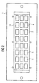
- Figure 2 shows a plan view of a mounting frame 1 with positioned plastic intermediate carrier 2, which is a variety of semiconductor chips 5 carries.
- the Device for packaging electronic components not yet the plastic grid according to the invention, which is shown in Fig. 1 can be seen, installed, so that the rows and columns Arrangement of the semiconductor chip positions 4 in the opening 14 of the mounting frame 1 can be seen.
- Figure 3 shows a plan view of a plastic grid 6, the in the first embodiment of the invention according to FIG. 1 is used due to the row and column arrangement the semiconductor chip positions 4 is the plastic grid constructed from cross and longitudinal webs 8 and 9.
- the width of the Crosspieces are wider than the saw blade width b, as shown in the figure 7 is shown.
- the cross and longitudinal webs 8 and 9 of the plastic grid 6 leave openings 16 free in their external dimensions are larger than the semiconductor chip dimensions of the semiconductor chips 5 at the semiconductor chip positions 4.
- the plastic grid for packaging electronic components on the plastic intermediate carrier 2, which is in Fig. 1 and 2nd is shown to be positioned. So that through Plastic grid 6 a part of the plastic molding compound 7 for packaging replaced by electronic components.
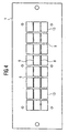
- Figure 4 shows a plan view of a mounting frame 1 a second embodiment of the invention. If for new designs an improved mounting frame 1 is to be constructed, can this be a one-piece integral component with the invention Form plastic grid 6.
- the invention in the Mounting frame 1 according to a second preferred embodiment the invention, as shown in Figure 4, a variety of Openings provided the dimensions in their dimensions of the semiconductor chips 5, as shown in FIG. 5, correspond.
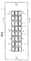
- Figure 5 shows a plan view of the mounting frame 1 of the figure 4 with a multiplicity of positioned semiconductor chips 5 in one Variety of openings 13 of the mounting frame 1.
- the Plastic intermediate carrier 2 is essentially in Figure 5 covered by the mounting frame 1 shown in Figure 4. Only the semiconductor chips 5 of the plastic intermediate carrier are in position within the plurality of openings 13 of the mounting frame 1 can be seen.
- Figure 6 shows a cross section of the second embodiment of the invention after the plastic molding compound 7 has been introduced along the sectional plane A-A of Figure 5 in cross section.
- the Mounting frame 1 and the plastic grid 6 are in this Embodiment of the same material and form a one-piece integral component that is a semiconductor chip with each opening 13 5 surrounds.
- the plastic intermediate carrier 2 with its Bumps 3 and the conductor tracks 4, not shown, carries the semiconductor chip 5 and the space between the semiconductor chip 5, mounting frame 1 or plastic grid 6 and plastic intermediate carrier 2 is with plastic casting compound 7, which in this embodiment consists of a silicone mass, filled.
- Figure 7 shows the cross section of the embodiment of Figure 6 with saw blades 15, the electronic in the separation step Separate components 11.
- the saw blade width b is smaller than the web width of the webs 8, 9, so that in the separation step A protective frame 12, as shown in Figure 8, is created.
- Figure 8 shows the cross section of the embodiment of Figure 6 after the separation step. After this step, isolated ones arise electronic components 11 with one by one Plastic frame 12 reinforced housing from which the bumps 3 protrude, and that the semiconductor chip 5 in its Edge area completely surrounded by plastic casting compound 7.
- plastic casting compound 7 By potting the device for packaging electronic Components with a plastic casting compound in a vacuum it also ensures that all voids between Semiconductor chip 5 and plastic intermediate carrier 2 with the Plastic casting compound 5 are filled, so that a dimensionally stable electronic component can be manufactured.
Landscapes
- Structures Or Materials For Encapsulating Or Coating Semiconductor Devices Or Solid State Devices (AREA)
- Encapsulation Of And Coatings For Semiconductor Or Solid State Devices (AREA)
Abstract
Description
Claims (20)
- Vorrichtung zum Verpacken von elektronischen Bauteilen mit Montagerahmen (1), der einen Kunststoffzwischenträger (2) umrahmt und hält, wobei der Kunststoffzwischenträger (2) an eine Vielzahl von Kontakthöckern (3) angeschließbare Leiterbahnen aufweist, die zu einer Vielzahl von Halbleiterchippositionen (4) innerhalb des Montagerahmens (1) führen und in diesen Positionen Halbleiterchips (5) aufweisen, deren Kontaktflächen mit den Leiterbahnen verbunden sind, während Abstandhalter aus Kunststoff die Halbleiterchips (5) auf dem Kunststoffzwischenträger (2) in den Halbleiterchippositionen (4) halten, wobei zusätzlich zu den Halbleiterchips (5) ein Kunststoffgitter (6) auf dem Kunststoffzwischenträger (2) angeordnet ist, welches jedes Halbleiterchip (5) rahmenartig umgibt und welches zum Verpacken der Vielzahl von Halbleiterchips mit einer Kunststoffgußmasse (7) zwischen Halbleiterchips (5) und Kunststoffgitter (6) versehen ist.
- Vorrichtung nach Anspruch 1,
dadurch gekennzeichnet, daß
die Kunststoffgußmasse (7) eine thermoplastische Siliconmasse ist. - Vorrichtung nach Anspruch 1 oder Anspruch 2,
dadurch gekennzeichnet, daß
der Montagerahmen (1) aus einem formstabilen Kunststoff oder einem Metall hergestellt ist. - Vorrichtung nach Anspruch 1 oder Anspruch 2,
dadurch gekennzeichnet, daß
der Montagerahmen (1) aus einem Duroplast hergestellt ist. - Vorrichtung nach einem der vorhergehenden Ansprüche,
dadurch gekennzeichnet, daß
der Montagerahmen (1) und das Kunststoffgitter (6) aus dem gleichen Material hergestellt sind. - Vorrichtung nach einem der vorhergehenden Ansprüche,
dadurch gekennzeichnet, daß
die Halbleiterchippositionen (4) auf dem Kunststoffzwischenträger (2) reihen- und spaltenweise angeordnet sind. - Vorrichtung nach einem der vorhergehenden Ansprüche,
dadurch gekennzeichnet, daß
der Kunststoffzwischenträger (2) bandförmig ist. - Vorrichtung nach einem der vorhergehenden Ansprüche,
dadurch gekennzeichnet, daß
der Kunststoffzwischenträger (2) aus einem flexiblen Polyamid mit zu Leiterbahnen strukturierter Metallbeschichtung hergestellt ist. - Vorrichtung nach einem der vorhergehenden Ansprüche,
dadurch gekennzeichnet, daß
das Kunststoffgitter (6) Längs-(8) und Querstege (9) aufweist, die breiter sind als eine Sägeblattbreite (b) einer Säge (10) zum Trennen der Halbleiterchippositionen (4) zu einzelnen verpackten elektronischen Bauteilen (11) mit Kontakthöckern (3). - Vorrichtung nach einem der vorhergehenden Ansprüche,
dadurch gekennzeichnet, daß
das Kunststoffgitter (6) einen Schutzrahmen (12) um jedes einzelne der Vielzahl von Halbleiterchips (5) bildet. - Vorrichtung nach einem der vorhergehenden Ansprüche,
dadurch gekennzeichnet, daß
der Montagerahmen (1) und das Kunststoffgitter (6) ein einstückiges integrales Bauteil sind mit Öffnungen (13) für jedes Halbleiterchip (5). - Vorrichtung nach einem der vorhergehenden Ansprüche,
dadurch gekennzeichnet, daß
der Montagerahmen (1), der die Öffnungen (13) für die Halbleiterchips (5) umgibt, breiter ist als eine Sägeblattbreite (b) einer Säge (10) zum Trennen der Halbleiterchippositionen (4) zu einzelnen verpackten elektronischen Bauteilen (11) mit Kontakthöckern (3). - Verfahren zum Verpacken von elektronischen Bauteilen (11) gemäß einem der Ansprüche 1 bis 12 mit folgenden Verfahrensschritten:Bereitstellen eines Montagerahmens (1) mit einer Öffnung (14) zum Einpassen eines streifenförmigen Kunststoffzwischenträgers (2),Bereitstellen eines Kunststoffzwischenträgers (2) für eine Vielzahl von Kontakthöckern (3) mit anschließbaren Leiterbahnen, die zu einer Vielzahl von Halbleiterchippositionen (4) führen und in diesen Positionen Halbleiterchips (5) aufweisen, deren Kontaktflächen mit den Leiterbahnen verbunden sind, während Abstandhalter aus Kunststoff die Vielzahl der Halbleiterchips (5) auf dem Kunststoffzwischenträger (1) in den Halbleiterchippositionen (4) halten,Positionieren der Vielzahl von Halbleiterchips (5) in der Öffnung (14) des Montagerahmens (1) unter Aufbringen des Kunststoffzwischenträgers (2) auf dem Montagerahmen (1),Positionieren eines Kunststoffgitters (6) auf dem Kunststoffzwischenträger (2), so daß die Vielzahl der Halbleiterchips (5) von dem Kunststoffgitter (6) rahmenartig umgeben wird,Versiegeln der Vielzahl von Halbleiterchips (5) durch Vergießen des Zwischenraums zwischen Halbleiterchips (5) und Kunststoffgitter (6) mit einer Kunststoffgußmasse (15), sowie aller Hohlräume zwischen Halbleiterchip (5) und Kunststoffzwischenträger (2) undTrennen des Kunststoffgitters (6) zu einzelnen jedes Halbleiterchip (5) umgebenden Schutzrahmen (12) unter Bilden eines verpackten elektronischen Bauteils (11) mit formstabilen Schutzrahmen (12).
- Verfahren zum Verpacken von elektronischen Bauteilen gemäß einem der Ansprüche 1 bis 12, gekennzeichnet durch folgende Verfahrensschritte:Bereitstellen eines Montagerahmens (1) mit einer Vielzahl von Öffnungen (13) zum Einpassen einer Vielzahl auf einem Kunststoffzwischenträger (2) an Halbleiterchippositionen (4) getragener Halbleiterchips (5) in die Öffnungen (13),Bereitstellen eines Kunststoffzwischenträgers (2) mit einer Vielzahl von Kontakthöckern (3) mit angeschlossenen Leiterbahnen, die zu einer Vielzahl von Halbleiterchippositionen (4) führen und in diesen Positionen Halbleiterchips (5) aufweisen, deren Kontaktflächen mit den Leiterbahnen verbunden sind, während Abstandhalter aus Kunststoff die Vielzahl der Halbleiterchips (5) auf dem Kunststoffzwischenträger (2) in den Halbleiterchippositionen (4) halten,Positionieren der Vielzahl von Halbleiterchips (5) in den Öffnungen (13) des Montagerahmens (1) unter Aufbringen des Kunststoffzwischenträgers (1) auf dem Montagerahmen (1), so daß jedes der Halbleiterchips (5) von dem Montagerahmen (1) umgeben wird,Verpacken der Vielzahl von Halbleiterchips (5) durch Vergießen des Zwischenraums mit einer Kunststoffgußmasse (7) zwischen Halbleiterchips (5) und Montagerahmen (1), sowie aller Hohlräume zwischen Halbleiterchip (1) und Kunststoffzwischenträger (2), undTrennen des Montagerahmens (1) zu einzelnen jedes Halbleiterchip (5) umgebenden Schutzrahmen (12) unter Bilden eines verpackten elektronischen Bauteils (11) mit Schutzrahmen (12).
- Verfahren nach Anspruch 13 oder 14,
dadurch gekennzeichnet, daß
als Kunststoffgußmasse (15) eine thermoplastische Siliconmasse eingesetzt wird. - Verfahren nach einem der Ansprüche 13 bis 15,
dadurch gekennzeichnet, daß
der Montagerahmen (1) aus einem formstabilen Kunststoff mittels eines Spriztgußverfahrens hergestellt wird. - Verfahren nach einem der Ansprüche 13 bis 16,
dadurch gekennzeichnet, daß
der Montagerahmen (1) aus einem Duroplast durch Mischen zweier Harzkomponenten hergestellt wird. - Verfahren nach einem der Ansprüche 13 bis 17,
dadurch gekennzeichnet, daß
der Montagerahmen (1) und das Kunststoffgitter (6) aus dem gleichen Material in einem Spritzgußverfahren hergestellt werden. - Verfahren nach einem der Ansprüche 13 bis 18,
dadurch gekennzeichnet, daß
der Kunststoffzwischenträger (2) aus einem flexiblen Polyamid mit zu Leiterbahnen strukturierter Metallbeschichtung, die mittels galvanischer Abscheidung und anschließender Strukturierung hergestellt wird. - Verfahren nach einem der Ansprüche 13 bis 19,
dadurch gekennzeichnet, daß
die Kontakthöcker (3) durch Anschmelzen von Lötkontaktkugeln hergestellt werden.
Applications Claiming Priority (2)
| Application Number | Priority Date | Filing Date | Title |
|---|---|---|---|
| DE10014380 | 2000-03-23 | ||
| DE10014380A DE10014380A1 (de) | 2000-03-23 | 2000-03-23 | Vorrichtung zum Verpacken von elektronischen Bauteilen |
Publications (2)
| Publication Number | Publication Date |
|---|---|
| EP1143508A2 true EP1143508A2 (de) | 2001-10-10 |
| EP1143508A3 EP1143508A3 (de) | 2004-06-23 |
Family
ID=7636012
Family Applications (1)
| Application Number | Title | Priority Date | Filing Date |
|---|---|---|---|
| EP01106481A Withdrawn EP1143508A3 (de) | 2000-03-23 | 2001-03-23 | Vorrichtung zum Verpacken von elektronischen Bauteilen |
Country Status (3)
| Country | Link |
|---|---|
| US (1) | US6521988B2 (de) |
| EP (1) | EP1143508A3 (de) |
| DE (1) | DE10014380A1 (de) |
Cited By (2)
| Publication number | Priority date | Publication date | Assignee | Title |
|---|---|---|---|---|
| DE10127009A1 (de) * | 2001-06-05 | 2002-12-12 | Infineon Technologies Ag | Kunststoffgehäuse mit mehreren Halbleiterchips und einer Umverdrahtungsplatte sowie ein Verfahren zur Herstellung des Kunststoffgehäuses in einer Spritzgußform |
| DE10154199A1 (de) * | 2001-11-07 | 2003-02-06 | Infineon Technologies Ag | Elektronisches Bauteil mit Halbleiterchip und Systemträger mit Bauteilpositionen und Verfahren zu deren Herstellung |
Families Citing this family (16)
| Publication number | Priority date | Publication date | Assignee | Title |
|---|---|---|---|---|
| US20060191215A1 (en) * | 2002-03-22 | 2006-08-31 | Stark David H | Insulated glazing units and methods |
| US6962834B2 (en) * | 2002-03-22 | 2005-11-08 | Stark David H | Wafer-level hermetic micro-device packages |
| US6627814B1 (en) * | 2002-03-22 | 2003-09-30 | David H. Stark | Hermetically sealed micro-device package with window |
| US7832177B2 (en) * | 2002-03-22 | 2010-11-16 | Electronics Packaging Solutions, Inc. | Insulated glazing units |
| DE10224124A1 (de) * | 2002-05-29 | 2003-12-18 | Infineon Technologies Ag | Elektronisches Bauteil mit äußeren Flächenkontakten und Verfahren zu seiner Herstellung |
| US20040187437A1 (en) * | 2003-03-27 | 2004-09-30 | Stark David H. | Laminated strength-reinforced window assemblies |
| US7265317B2 (en) * | 2004-01-28 | 2007-09-04 | Boston Scientific Scimed, Inc. | Method of cutting material with hybrid liquid-jet/laser system |
| US20050257877A1 (en) * | 2004-04-19 | 2005-11-24 | Stark David H | Bonded assemblies |
| KR100645897B1 (ko) | 2005-07-22 | 2006-11-14 | 세크론 주식회사 | 비지에이 패키지의 소잉소터시스템 및 방법 |
| US7989040B2 (en) | 2007-09-14 | 2011-08-02 | Electronics Packaging Solutions, Inc. | Insulating glass unit having multi-height internal standoffs and visible decoration |
| WO2010019484A2 (en) | 2008-08-09 | 2010-02-18 | Eversealed Windows, Inc. | Asymmetrical flexible edge seal for vacuum insulating glass |
| US8512830B2 (en) | 2009-01-15 | 2013-08-20 | Eversealed Windows, Inc. | Filament-strung stand-off elements for maintaining pane separation in vacuum insulating glazing units |
| US8329267B2 (en) | 2009-01-15 | 2012-12-11 | Eversealed Windows, Inc. | Flexible edge seal for vacuum insulating glazing units |
| US8950162B2 (en) | 2010-06-02 | 2015-02-10 | Eversealed Windows, Inc. | Multi-pane glass unit having seal with adhesive and hermetic coating layer |
| US9328512B2 (en) | 2011-05-05 | 2016-05-03 | Eversealed Windows, Inc. | Method and apparatus for an insulating glazing unit and compliant seal for an insulating glazing unit |
| DE102021119190A1 (de) * | 2021-07-23 | 2023-01-26 | Infineon Technologies Ag | Verfahren zum Herstellen einer Dokumentenstruktur und Dokumentenstruktur |
Family Cites Families (13)
| Publication number | Priority date | Publication date | Assignee | Title |
|---|---|---|---|---|
| US5023202A (en) * | 1989-07-14 | 1991-06-11 | Lsi Logic Corporation | Rigid strip carrier for integrated circuits |
| JPH07106638A (ja) * | 1993-09-30 | 1995-04-21 | Rohm Co Ltd | チップ型発光ダイオードの製造方法 |
| TW272311B (de) * | 1994-01-12 | 1996-03-11 | At & T Corp | |
| US5467253A (en) * | 1994-06-30 | 1995-11-14 | Motorola, Inc. | Semiconductor chip package and method of forming |
| US5612513A (en) * | 1995-09-19 | 1997-03-18 | Micron Communications, Inc. | Article and method of manufacturing an enclosed electrical circuit using an encapsulant |
| JP2867954B2 (ja) * | 1996-05-20 | 1999-03-10 | 日本電気株式会社 | チップ型半導体装置の製造方法 |
| US5990545A (en) * | 1996-12-02 | 1999-11-23 | 3M Innovative Properties Company | Chip scale ball grid array for integrated circuit package |
| JPH10284525A (ja) * | 1997-04-03 | 1998-10-23 | Shinko Electric Ind Co Ltd | 半導体装置の製造方法 |
| JP3859318B2 (ja) * | 1997-08-29 | 2006-12-20 | シチズン電子株式会社 | 電子回路のパッケージ方法 |
| JPH1197466A (ja) * | 1997-09-18 | 1999-04-09 | Miyota Kk | Icチップのパッケージ方法 |
| JPH11219959A (ja) * | 1998-02-03 | 1999-08-10 | Hitachi Cable Ltd | 半導体装置製造用キャリア |
| JP3127889B2 (ja) * | 1998-06-25 | 2001-01-29 | 日本電気株式会社 | 半導体パッケージの製造方法およびその成形用金型 |
| JP3825181B2 (ja) * | 1998-08-20 | 2006-09-20 | 沖電気工業株式会社 | 半導体装置の製造方法及び半導体装置 |
-
2000
- 2000-03-23 DE DE10014380A patent/DE10014380A1/de not_active Withdrawn
-
2001
- 2001-03-23 US US09/816,929 patent/US6521988B2/en not_active Expired - Lifetime
- 2001-03-23 EP EP01106481A patent/EP1143508A3/de not_active Withdrawn
Cited By (2)
| Publication number | Priority date | Publication date | Assignee | Title |
|---|---|---|---|---|
| DE10127009A1 (de) * | 2001-06-05 | 2002-12-12 | Infineon Technologies Ag | Kunststoffgehäuse mit mehreren Halbleiterchips und einer Umverdrahtungsplatte sowie ein Verfahren zur Herstellung des Kunststoffgehäuses in einer Spritzgußform |
| DE10154199A1 (de) * | 2001-11-07 | 2003-02-06 | Infineon Technologies Ag | Elektronisches Bauteil mit Halbleiterchip und Systemträger mit Bauteilpositionen und Verfahren zu deren Herstellung |
Also Published As
| Publication number | Publication date |
|---|---|
| US6521988B2 (en) | 2003-02-18 |
| US20010045641A1 (en) | 2001-11-29 |
| DE10014380A1 (de) | 2001-10-04 |
| EP1143508A3 (de) | 2004-06-23 |
Similar Documents
| Publication | Publication Date | Title |
|---|---|---|
| EP1143508A2 (de) | Vorrichtung zum Verpacken von elektronischen Bauteilen | |
| DE69737248T2 (de) | Verfahren zum Einkapseln einer integrierten Halbleiterschaltung | |
| DE2931449C2 (de) | ||
| DE3814469C2 (de) | ||
| DE4318727C2 (de) | Verfahren zur Herstellung einer Halbleitervorrichtung mit LOC-Struktur sowie dazugehöriger Zuführungsdrahtrahmen | |
| DE68928185T2 (de) | Herstellung elektronischer Bauelemente mit Hilfe von Leiterrahmen | |
| DE69534483T2 (de) | Leiterrahmen und Halbleiterbauelement | |
| DE102004013056B4 (de) | Verfahren zur Herstellung eines Halbleiterbauelements | |
| DE10229182A1 (de) | Gestapelte Chip-Packung und Herstellungsverfahren hierfür | |
| DE10222608B4 (de) | Halbleitervorrichtung und Verfahren zum Herstellen derselben | |
| CH686325A5 (de) | Elektronikmodul und Chip-Karte. | |
| DE102013103580B4 (de) | Dreidimensional gestapelte Gehäuseanordnung und Verfahren zum Herstellen derselben | |
| DE102013224581A1 (de) | Optoelektronisches Bauelement und Verfahren zu seiner Herstellung | |
| DE2363833C2 (de) | Verfahren zum elektrischen und mechanischen Verbinden einer Vielzahl von mit streifenförmigen Leitern (beamlead) kontaktierten Halbleiterchips mit jeweils einem äußeren Leiterrahmen | |
| DE102014100509A1 (de) | Verfahren zur herstellung und testung eines chipgehäuses | |
| DE102012104882B4 (de) | Verfahren zur Herstellung von optoelektronischen Halbleiterbauteilen und damit hergestelltes optoelektronisches Halbleiterbauteil | |
| DE10127009A1 (de) | Kunststoffgehäuse mit mehreren Halbleiterchips und einer Umverdrahtungsplatte sowie ein Verfahren zur Herstellung des Kunststoffgehäuses in einer Spritzgußform | |
| DE69609921T2 (de) | Herstellungsverfahren einer halbleiteranordnung geeignet zur oberflächenmontage | |
| DE10206661A1 (de) | Elektronisches Bauteil mit einem Halbleiterchip | |
| DE102015107232A1 (de) | Verfahren zur Vereinzelung von Packages und Leadframe | |
| DE112016000307B4 (de) | Leiterrahmen und Verfahren zum Herstellen eines Chipgehäuses sowie Verfahren zum Herstellen eines optoelektronischen Bauelements | |
| DE19609113A1 (de) | Anguß-Trennvorrichtung und Anguß-Trennverfahren | |
| DE69317373T2 (de) | Hohlgeformte Plastikpackung für Halbleiteranordnung und Herstellungsverfahren | |
| DE19929215A1 (de) | Verfahren zur Herstellung eines BGA-Halbleiterbauelements, ein TAB-Band für ein BGA-Halbleiterbauelement und ein BGA-Halbleiterbauelement | |
| DE112006003664B4 (de) | Herstellung eines QFN-Gehäuses für eine integrierte Schaltung und damit hergestelltes QFN-Gehäuse und Verwendung eines Leiterrahmens dabei |
Legal Events
| Date | Code | Title | Description |
|---|---|---|---|
| PUAI | Public reference made under article 153(3) epc to a published international application that has entered the european phase |
Free format text: ORIGINAL CODE: 0009012 |
|
| AK | Designated contracting states |
Kind code of ref document: A2 Designated state(s): AT BE CH CY DE DK ES FI FR GB GR IE IT LI LU MC NL PT SE TR |
|
| AX | Request for extension of the european patent |
Free format text: AL;LT;LV;MK;RO;SI |
|
| PUAL | Search report despatched |
Free format text: ORIGINAL CODE: 0009013 |
|
| AK | Designated contracting states |
Kind code of ref document: A3 Designated state(s): AT BE CH CY DE DK ES FI FR GB GR IE IT LI LU MC NL PT SE TR |
|
| AX | Request for extension of the european patent |
Extension state: AL LT LV MK RO SI |
|
| 17P | Request for examination filed |
Effective date: 20040802 |
|
| AKX | Designation fees paid |
Designated state(s): DE |
|
| RBV | Designated contracting states (corrected) |
Designated state(s): DE |
|
| 17Q | First examination report despatched |
Effective date: 20070927 |
|
| STAA | Information on the status of an ep patent application or granted ep patent |
Free format text: STATUS: THE APPLICATION IS DEEMED TO BE WITHDRAWN |
|
| 18D | Application deemed to be withdrawn |
Effective date: 20080208 |