EP1142125B1 - System zur quantisierung eines analogen signals mit einer brücke von dioden mit resonantem tunneleffekt - Google Patents
System zur quantisierung eines analogen signals mit einer brücke von dioden mit resonantem tunneleffekt Download PDFInfo
- Publication number
- EP1142125B1 EP1142125B1 EP00905537A EP00905537A EP1142125B1 EP 1142125 B1 EP1142125 B1 EP 1142125B1 EP 00905537 A EP00905537 A EP 00905537A EP 00905537 A EP00905537 A EP 00905537A EP 1142125 B1 EP1142125 B1 EP 1142125B1
- Authority
- EP
- European Patent Office
- Prior art keywords
- terminal
- bridge
- clock
- amplifier
- input
- Prior art date
- Legal status (The legal status is an assumption and is not a legal conclusion. Google has not performed a legal analysis and makes no representation as to the accuracy of the status listed.)
- Expired - Lifetime
Links
Images

Classifications
-
- H—ELECTRICITY
- H03—ELECTRONIC CIRCUITRY
- H03M—CODING; DECODING; CODE CONVERSION IN GENERAL
- H03M1/00—Analogue/digital conversion; Digital/analogue conversion
- H03M1/12—Analogue/digital converters
- H03M1/34—Analogue value compared with reference values
-
- B—PERFORMING OPERATIONS; TRANSPORTING
- B82—NANOTECHNOLOGY
- B82Y—SPECIFIC USES OR APPLICATIONS OF NANOSTRUCTURES; MEASUREMENT OR ANALYSIS OF NANOSTRUCTURES; MANUFACTURE OR TREATMENT OF NANOSTRUCTURES
- B82Y10/00—Nanotechnology for information processing, storage or transmission, e.g. quantum computing or single electron logic
-
- H—ELECTRICITY
- H03—ELECTRONIC CIRCUITRY
- H03M—CODING; DECODING; CODE CONVERSION IN GENERAL
- H03M1/00—Analogue/digital conversion; Digital/analogue conversion
- H03M1/06—Continuously compensating for, or preventing, undesired influence of physical parameters
- H03M1/0617—Continuously compensating for, or preventing, undesired influence of physical parameters characterised by the use of methods or means not specific to a particular type of detrimental influence
- H03M1/0675—Continuously compensating for, or preventing, undesired influence of physical parameters characterised by the use of methods or means not specific to a particular type of detrimental influence using redundancy
- H03M1/0678—Continuously compensating for, or preventing, undesired influence of physical parameters characterised by the use of methods or means not specific to a particular type of detrimental influence using redundancy using additional components or elements, e.g. dummy components
- H03M1/068—Continuously compensating for, or preventing, undesired influence of physical parameters characterised by the use of methods or means not specific to a particular type of detrimental influence using redundancy using additional components or elements, e.g. dummy components the original and additional components or elements being complementary to each other, e.g. CMOS
- H03M1/0682—Continuously compensating for, or preventing, undesired influence of physical parameters characterised by the use of methods or means not specific to a particular type of detrimental influence using redundancy using additional components or elements, e.g. dummy components the original and additional components or elements being complementary to each other, e.g. CMOS using a differential network structure, i.e. symmetrical with respect to ground
Definitions
- This invention relates generally to electronic quantizing and more particularly to a system for quantizing an analog signal utilizing a resonant tunneling diode bridge.
- Analog-to-digital converters have been formed in a variety of architectures. Conventionally, these architectures have been implemented with transistors. For example, one common implementation includes a cross-coupled pair of transistors. However, there are several disadvantages associated with using transistors to implement an analog-to-digital converter.
- This object can be achieved by a system for quantizing an analog signal with the features of independent claim 1.
- a system for quantizing an analog signal utilizing a resonant tunneling diode bridge is provided that substantially eliminates or reduces the disadvantages or problems associated with previously developed quantizers.
- a system for quantizing an analog signal comprises a first negative-resistance device.
- the first negative-resistance device has a first terminal coupled to receive a clock signal and a second terminal coupled to receive a first input signal.
- a second negative-resistance device has a first terminal coupled to receive the clock signal and a second terminal coupled to receive a second input signal.
- a third negative-resistance device has a first terminal coupled to receive the first input signal and a second terminal coupled to receive the inverted clock signal.
- a fourth negative-resistance device has a first terminal coupled to receive the second input signal and a second terminal coupled to receive the inverted clock signal.
- An output terminal is coupled to the second terminal of the first negative-resistance device and the first terminal of the third negative-resistance device.
- the output terminal provides an output signal.
- An inverted output terminal is coupled to the second terminal of the second negative-resistance device and the first terminal of the fourth negative-resistance device. The inverted output terminal provides an inverted output signal.
- a negative-resistance element such as a resonant tunneling diode is included as a part of the analog-to-digital converter. Accordingly, reliance on transistors is avoided. As a result, the detrimental effects of quantum mechanics are minimized or not present, switching speed is increased, and use of multi-valued logic is possible.
- FIGURES 1 through 10 of the drawings in which like numerals refer to like parts.
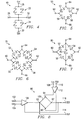
- FIGURE 1 is a schematic diagram of a resonant tunneling diode (RTD) 10 for use as a negative-resistance element in accordance with the teachings of the present invention.
- RTD 10 comprises an input terminal 11 for receiving an input signal, an output terminal 12 for producing an output signal, two tunnel barrier layers 13, and a quantum well layer 14.
- FIGURE 2 is a graph showing current as a function of voltage for a negative-resistance element such as an RTD 10.
- the shape of this I-V curve is determined by the quantum effects that are a result of the extreme thinness of tunnel barrier layers 13 and quantum well layer 14. These layers 13 and 14 are approximately ten (10) to twenty (20) atoms thick.
- RTD 10 This property of negative-resistance elements such as RTDs 10 that allows switching back and forth between on and off states as the voltage increases enables biasing to operate in one of three stable states, as illustrated in FIGURE 2. These three stable states are the negative-bias valley region 16, the pre-peak region 17, and the positive-bias valley region 18.
- tunnel barrier layers 13 and quantum well layer 14 of RTD 10 Another property associated with the extreme thinness of tunnel barrier layers 13 and quantum well layer 14 of RTD 10 relates to switching speed. Because each of these layers 13 and 14 are only about ten (10) to twenty (20) atoms thick, an electron only travels about .01 microns from input terminal 11 to output terminal 12. Because of this short distance, RTD 10 switches on and off at a very high rate.
- FIGURES 3 and 4 are circuit diagrams illustrating systems 20 and 40 for quantizing an analog signal in accordance with the present invention.
- Systems 20 and 40 comprise a first resonant tunneling diode(s) 22 and a second resonant tunneling diode(s) 24.
- Systems 20 and 40 also comprise an input terminal 26 for receiving an analog input signal, a clock terminal 28 for receiving a clock signal, an inverted clock terminal 30 for receiving an inverted clock signal, and an output terminal 32 for producing a quantized output signal.
- the input received at input terminal 26 comprises a current varying signal
- the output at output terminal 32 comprises a voltage varying signal.
- the input signal varies in the X-band range (ten or more gigahertz).
- the RTDs 22 and 24 are biased the same with respect to the clock terminal 28.
- the RTDs 22 and 24 each comprise a pair connected in parallel and biased oppositely to each other.
- the RTDs operate in the pre-peak region 17 when the input current is zero. This produces an output signal of zero voltage. However, when the input current reaches a specified level, one of the RTDs 22 or 24 is forced by the resultant asymmetry into either the negative-bias valley region 16, resulting in an output signal of -1, or the positive-bias valley region 18, resulting in an output signal of +1.
- the output terminal 32 produces a +1 voltage signal for the output when the input signal is greater than a first threshold, a -1 voltage signal for the output when the input signal is less than a second threshold, and a zero voltage signal for the output when the input signal is between the first and second thresholds.
- the system 20 comprises a single RTD 22 and a single RTD 24.
- This embodiment provides a more compact layout and operates at a higher speed than the embodiment shown in FIGURE 4, wherein each of the RTDs 22 and 24 comprises a pair.
- the embodiment shown in FIGURE 4 provides more symmetry and reduces even-order harmonics that may exist in the embodiment shown in FIGURE 3.
- FIGURES 5, 6 and 7 are circuit diagrams illustrating bridges 50, 70 and 80 for quantizing an analog signal in accordance with the present invention.
- Bridges 50, 70 and 80 comprise a first resonant tunneling diode(s) 52, a second resonant tunneling diode(s) 54, a third resonant tunneling diode(s) 56, and a fourth resonant tunneling diode(s) 58.
- Bridges 50, 70 and 80 also comprise an input terminal 60 for receiving an analog input signal, an inverted input terminal 62 for receiving an inverted input signal, a clock terminal 64 for receiving a clock signal, and an inverted clock terminal 66 for receiving an inverted clock signal.
- the inverted input terminal 62 for receiving an inverted input signal may be a reference terminal for receiving a reference signal.
- each RTD 52, 54, 56 and 58 is biased the same with respect to the clock terminal 64.
- each RTD 52, 54, 56 and 58 comprises a diode pair in parallel and biased oppositely to each other.
- the system 80 shown in FIGURE 7 comprises a fifth resonant tunneling diode 82.
- each RTD 52, 54, 56, 58 and 82 is biased the same with respect to the clock terminal 64.
- each RTD 52, 54, 56, 58 and 82 may comprise an RTD pair in parallel and biased oppositely to each other.
- the RTDs 52, 54, 56 and 58 operate in the pre-peak region 17, see FIGURE 2, when the input current is zero. This produces an output signal of zero. However, when the input current reaches a specified level, an asymmetry results producing an output signal of -1 or +1.
- a determination regarding whether the output signal will be -1 or +1 is made when the clock signal level increases.
- bridges 50 and 70 become positively biased and two of the RTDs 52, 54, 56 and 58 operate in either the negative-bias valley region 16, producing an output signal of -1 volts, or the positive-bias valley region 18, producing an output signal of +1 volts.
- the RTD 58 will also switch.
- the RTD 54 will be the second one to switch.
- the RTDs 52 and 58 switch, the output signal will be +1 volts, while if the RTDs 54 and 56 switch, the output signal will be -1 volts.
- a determination regarding whether the output signal will be -1 or +1 is also made when the clock signal level decreases.
- bridges 50 and 70 become negatively biased and two of the RTDs 52, 54, 56, and 58 are forced into either the negative-bias valley region 16, see FIGURE 2, or the positive-bias valley region 18 as just described in connection with a clock signal increase.
- either the RTDs 52 and 58 or the RTDs 54 and 56 will switch. In this case, however, if the RTDs 52 and 58 switch, the output signal will be -1, while if RTDs 54 and 56 switch, the output signal will be +1.
- the fifth RTD 82 creates an asymmetry that forces one of the pair of RTDs either 52 and 58 or 54 and 56 into the negative-bias valley region 16 or the positive-bias valley region 18. In this configuration, there is essentially no input signal that will result in an output signal of zero. Thus, for the embodiment in which the bridge 80 comprises a fifth RTD, the output signal produced will be binary instead of ternary.
- bridge 80 operates to determine the value of the output signal both when the clock increases and when the clock decreases. Therefore, bridges 50, 70 and 80 produce two outputs for each clock cycle. Thus, in order to obtain 25 gigasamples per second, for example, a 12.5 gigahertz clock is sufficient.
- FIGURES 5 and 7 where single RTDs 52, 54, 56, 58 and RTD 82 in Figure 7 comprise the bridge, a more compact layout is provided that operates at a higher speed than the embodiment shown in FIGURE 6, where each RTD 52, 54, 56 and 58 comprises a pair.
- the embodiment shown in FIGURE 6 provides more symmetry and reduces even-order harmonics that may exist in the embodiments shown in FIGURES 5 and 7.
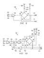
- FIGURE 8 is a circuit diagram illustrating a system 90 for quantizing an analog signal in a direct drive mode.
- System 90 comprises a bridge 100 configured according to one of the embodiments shown in FIGURES 5, 6 or 7.
- bridge 100 comprises an input terminal 60 for receiving an analog input signal, an inverted input terminal 62 for receiving an inverted input signal, a clock terminal 64 for receiving a clock signal, and an inverted clock terminal 66 for receiving an inverted clock signal.
- the inverted input terminal 62 for receiving an inverted input signal may be a reference terminal for receiving a reference signal.
- the input comprises a voltage varying signal received at a system input terminal 102.
- the inverted input signal is received at system input terminal 104.
- the input signal and the inverted input signal are applied to an input amplifier 106 having an output connected to the input terminal 60 and the inverted input terminal 62, respectively.
- the clock signal is received at clock input terminal 108 and the inverted clock signal is received at a clock input terminal 110.
- the clock signal and the inverted clock signal are applied to a clock amplifier 112 having one output applied to the clock terminal 64 and a second output applied to the inverted clock terminal 66, respectively.
- An output signal from system 90 is provided at a system output terminal 114 and an inverted system output is provided at an inverted system output terminal 116.
- the output comprises a signal varying with current.
- the system output terminal 114 is coupled to the input terminal 60 of the bridge 100, and the inverted system output terminal 116 is coupled to the inverted input terminal 62 of the bridge 100.
- the output signal comprises three levels represented by -1, 0, and +1.
- the input amplifier 106 amplifies the input signal and the inverted input signal
- the clock amplifier 112 amplifies the clock signal. With this amplification, a +1 is produced for the output signal when the input signal is greater than a first threshold, a -1 for the output signal when the input signal is less than a second threshold, and a zero for the output signal when the input signal is between the first and second thresholds.
- the output signal comprises one of two levels represented by -1 and +1.
- the input amplifier 106 amplifies the input signal and the inverted input signal
- the clock amplifier 112 amplifies the clock signal and the inverted clock signal. With this amplification, a +1 is produced for the output signal when the input signal is greater than a first threshold, and a -1 for the output signal when the input signal is less than a second threshold.
- FIGURE 9 is a circuit diagram illustrating a system 120 for quantizing an analog signal in a capacitive-coupled drive mode.
- System 120 comprises a bridge 100 configured according to one of the embodiments shown in FIGURES 5, 6 or 7.
- bridge 100 comprises an input terminal 60 for receiving an analog input signal, an inverted input terminal 62 for receiving an inverted input signal, a clock terminal for receiving a clock signal, and an inverted clock terminal 66 for receiving an inverted clock signal.
- the inverted input terminal 62 for receiving an inverted input signal may be a reference terminal for receiving a reference signal.
- the input comprises a current varying signal received at the system input terminal 102.
- the inverted input signal is received at the system input terminal 104.
- the input signal and the inverted input signal are applied to the input amplifier 106 having outputs connected to the input terminal 60 and inverted input terminal 62, respectively.
- the clock signal is received at the clock input terminal 108 and the inverted clock signal is received at the clock input terminal 110.
- the clock signal and the inverted clock signal are applied to resistors 124 and capacitors 126 and then connected to the clock terminal 64 and inverted clock terminal 66, respectively.
- An output signal is provided from the system 120 at a system output terminal 114 and an inverted output signal is provided at an inverted system output terminal 116.
- the output comprises a voltage varying signal.
- the system output terminal 114 is coupled to the bridge 100 at the input terminal 60, and the inverted system output terminal 116 is coupled to the bridge 100 at the inverted input terminal 62.
- the output comprises one of two levels represented by -1 and +1 independent of whether bridge 100 is configured in accordance with the embodiment shown in FIGURE 5, 6 or 7.
- the input amplifier 106 amplifies the input signal and the inverted input signal.
- the output signal at the system output 114 is +1 when the input signal is greater than a first threshold and a -1 when the input signal is less than a second threshold.
- FIGURE 10 is a circuit diagram illustrating a continuous-time modulator 130 in accordance with the present invention.
- Modulator 130 comprises a bridge 100 according to one of the embodiments shown in FIGURES 5, 6 or 7.
- bridge 100 comprises an input terminal 60 for receiving an analog input signal, an inverted input terminal 62 for receiving an inverted input signal, a clock terminal 64 for receiving a clock signal, and an inverted clock terminal 66 for receiving an inverted clock signal.
- the inverted input terminal 62 for receiving an inverted input signal may be a reference terminal for receiving a reference signal.
- the input comprises a current varying signal and is received at a system input terminal 132.
- the inverted input signal is received at a system input terminal 133.
- the input signal and the inverted input signal are applied to an input amplifier 134 having outputs on connecting lines 136 and 138, respectively.
- the lines 136 and 138 are connected to terminals 140 and 142, respectively, of a bridge amplifier 144 having outputs on lines connecting 146 and 148.
- the connecting lines 146 and 148 are connected to the input terminal 60 and inverted input terminal 62, respectively.
- Also connected to the input terminal 60 and inverted input terminal 62 are connecting lines 150 and 152, respectively.
- connecting lines apply the signals at terminals 60 and 62 to a feedback amplifier 154 having outputs on connecting lines 156 and 158.
- the connecting lines 156 and 158 are coupled to terminals 140 and 142, respectively, to feedback the bridge signals to the bridge amplifier 144.
- a capacitor 160 provides capacitive coupling between the connecting lines 136 and 138.
- the clock signal is received at a clock input terminal 162 and the inverted clock signal is received at an inverted clock input terminal 164.
- the clock signal and the inverted clock signal are applied to a clock amplifier 166 having outputs on connecting lines 168 and 170, respectively.
- the connecting lines 168 and 170 are tied to the clock terminal 64 and inverted clock terminal 66, respectively.
- the modulator 130 comprises an output terminal 172 for the output signal and an inverted output terminal 174 for the inverted output signal.
- the output comprises a voltage varying signal.
- Output terminal 172 is coupled to the bridge 100 at the input terminal 60, and the inverted output terminal 174 is coupled to the bridge 100 at the inverted input terminal 62.
- the output signal comprises one of three levels represented by -1, 0, and +1.
- input amplifier 134 amplifies the input signal and the inverted input signal
- the bridge amplifier 144 amplifies the signals received at terminals 140 and 142
- the feedback amplifier 154 amplifies the signals received on the connecting lines 150 and 152
- the clock amplifier 166 amplifies the clock signal and the inverted clock signal.
- the output signal at the terminal 172 is +1 when the input signal is greater than a first threshold, a -1 when the input signal is less than a second threshold, and a zero when the input signal is between the first and second thresholds.
- the output signal comprises one of two levels represented by -1 and +1.
- the input amplifier 134 amplifies signals applied thereto
- bridge amplifier 144 amplifies received signals
- feedback amplifier 154 amplifies inputs thereto
- clock amplifier 166 amplifies the clock signals.
- the output signal is a +1 when the input signal is greater than a first threshold and a -1 when the input signal is less than a second threshold.
- the amplification of clock amplifier 166 is about four to ten times greater than the amplification of bridge amplifier 144. This boosts the digital signal thereby reducing the analog feedback in comparison. This also reduces output resistance and increases both speed and sensitivity.
Landscapes
- Engineering & Computer Science (AREA)
- Theoretical Computer Science (AREA)
- Chemical & Material Sciences (AREA)
- Nanotechnology (AREA)
- Physics & Mathematics (AREA)
- Mathematical Physics (AREA)
- Crystallography & Structural Chemistry (AREA)
- Amplifiers (AREA)
- Analogue/Digital Conversion (AREA)
- Radar Systems Or Details Thereof (AREA)
- Digital Transmission Methods That Use Modulated Carrier Waves (AREA)
- Arrangements For Transmission Of Measured Signals (AREA)
Claims (21)
- System zum Quantisieren eines Analogsignals, umfassend:eine Quantisierungsbrücke (100) mit einem Brückeneingangsanschluß (60), einem invertierten Brückeneingangsanschluß (62), einem Taktanschluß (64) und einem invertierten Taktanschluß (66);eine erste Koppeleinrichtung (108), die ein Taktsignal empfängt, wobei die Brücke (100) so geschaltet ist, daß sie das Ausgangssignal der ersten Koppeleinrichtung (108) empfängt;eine zweite Koppeleinrichtung (110), die ein invertiertes Taktsignal empfängt, wobei die Brücke (100) so geschaltet ist, daß sie das Ausgangssignal der zweiten Koppeleinrichtung (110) empfängt;einen Ausgangsanschluß (114), der ein Ausgangssignal liefert, wobei der Ausgangsanschluß (114) an den Brückeneingangsanschluß (60) gekoppelt ist; undeinen invertierten Ausgangsanschluß (116), wobei der invertierte Ausgangsanschluß (116) an den invertierten Brückeneingangsanschluß (62) gekoppelt ist;dadurch gekennzeichnet, daß die Quantisierungsbrücke (100) weiterhin folgendes umfaßt:einen Eingangsverstärker (106), der ein erstes Eingangssignal und ein zweites Eingangssignal zu deren Verstärkung empfängt, wobei der Eingangsverstärker (106) an die Brücke (100) angelegte Ausgänge aufweist;eine erste Negativwiderstandseinrichtung (52) mit einem an den Taktanschluß (64) gekoppelten ersten Anschluß undeinen an den Brückeneingangsanschluß (60) gekoppelten zweiten Anschluß;eine zweite Negativwiderstandseinrichtung (54) mit einem an den Taktanschluß (64) gekoppelten ersten Anschluß undeinen an den invertierten Brückeneingangsanschluß (62) gekoppelten zweiten Anschluß;eine dritte Negativwiderstandseinrichtung (56) mit einem an den Brückeneingangsanschluß (60) gekoppelten ersten Anschluß und einen an den invertierten Taktanschluß (66) gekoppelten zweiten Anschluß; undeine vierte Negativwiderstandseinrichtung (58) mit einem an den invertierten Brückeneingangsanschluß (62) gekoppelten ersten Anschluß und einen an den invertierten Taktanschluß (66) gekoppelten zweiten Anschluß.
- System (120) nach Anspruch 1, das weiterhin folgendes umfaßt:einen zwischen den Eingangsverstärker (106) und die Brücke (100) gekoppelten Brückenverstärker (144) zum Empfangen verstärkter Signale von dem Eingangsverstärker (106), wobei der Brückenverstärker (144) an die Brücke (100) angelegte Ausgänge aufweist.
- System (120) nach Anspruch 1 oder 2, wobei die erste, zweite, dritte und vierte Negativwiderstandseinrichtung (52, 54, 56, 58) jeweils eine Resonanzeffekt-Tunneldiode umfassen.
- System (120) nach einem der vorhergehenden Ansprüche, weiterhin mit Mitteln zum gleichen Vorspannen der ersten, zweiten, dritten und vierten Negativwiderstandseinrichtung (52, 54, 56, 58) bezüglich des Taktsignals.
- System (120) nach einem der vorhergehenden Ansprüche, wobei die erste, zweite, dritte und vierte Negativwiderstandseinrichtung (52, 54, 56, 58) jeweils eine erste Resonanzeffekt-Tunneldiode parallel zu einer zweiten Resonanzeffekt-Tunneldiode umfassen und wobei die erste Resonanzeffekt-Tunneldiode entgegen der zweiten Resonanzeffekt-Tunneldiode vorgespannt ist.
- System (120) nach einem der vorhergehenden Ansprüche, weiterhin mit einer fünften Negativwiderstandseinrichtung (82) mit einem ersten Anschluß, der gekoppelt ist, um das Taktsignal zu empfangen, und einem zweiten Anschluß, der gekoppelt ist, um das invertierte Taktsignal zu empfangen.
- System (120) nach einem der vorhergehenden Ansprüche, wobei die erste und zweite Koppeleinrichtung (108, 110) Teil eines Taktverstärkers (112) mit einem ersten Eingangsanschluß, einem zweiten Eingangsanschluß, einem ersten Ausgangsanschluß und einem zweiten Ausgangsanschluß sind;
Mittel zum Koppeln des Taktsignals an den ersten Eingangsanschluß des Taktverstärkers (112);
Mittel zum Koppeln des invertierten Taktsignals an den zweiten Eingangsanschluß des Taktverstärkers (112);
Mittel zum Koppeln des ersten Ausgangsanschlusses des Taktverstärkers (112) an den ersten Anschluß der ersten Negativwiderstandseinrichtung (52) und den ersten Anschluß der zweiten Negativwiderstandseinrichtung (54) und
Mittel zum Koppeln des zweiten Ausgangsanschlusses des Taktverstärkers (112) an den zweiten Anschluß der dritten Negativwiderstandseinrichtung (56) und den zweiten Anschluß der vierten Negativwiderstandseinrichtung (58). - System (120) nach Anspruch 1, wobei die erste und zweite Koppeleinrichtung (108, 110) von einem Taktverstärker (112) vorgesehen werden, wobei der Taktverstärker (112) ein Taktsignal und ein invertiertes Taktsignal zu deren Verstärkung empfängt, wobei die Brücke (100) gekoppelt ist, um die Ausgangssignale des Taktverstärkers (112) zu empfangen.
- System (120) nach Anspruch 8, das weiterhin folgendes umfaßt:
einen zwischen den Eingangsverstärker (106) und die Brücke (100) gekoppelten Brückenverstärker (144) zum Empfangen verstärkter Signale von dem Eingangsverstärker (106), wobei der Brückenverstärker (144) an die Brücke (100) angelegte Ausgänge aufweist. - System (120) nach Anspruch 1, wobei die erste Koppeleinrichtung (108) und die zweite Koppeleinrichtung (110) jeweils einen mit einem Kondensator (126) in Reihe geschalteten Widerstand (124) umfassen.
- System (120) nach Anspruch 1, weiterhin umfassend:einen Rückkopplungsverstärker (154), der gekoppelt ist, um Ausgangssignale von der Brücke (100) zu empfangen, wobei der Rückkopplungsverstärker (154) an die Brücke (100) angelegte Ausgänge aufweist.
- System (120) nach Anspruch 11, das weiterhin folgendes umfaßt:
einen zwischen den Eingangsverstärker (106) und die Brücke (100) gekoppelten Brückenverstärker (144) zum Empfangen verstärkter Signale von dem Eingangsverstärker (106), wobei der Brückenverstärker (144) an die Brücke (100) angelegte Ausgänge aufweist, wobei der Rückkopplungsverstärker (154) an den Brückenverstärker (144) angelegte Ausgänge aufweist. - System (120) nach Anspruch 12, wobei der Brückenverstärker (144) weiterhin einen ersten Eingangsanschluß und einen zweiten Eingangsanschluß umfaßt und weiterhin einen Kondensator (160) mit einem an den ersten Eingangsanschluß gekoppelten ersten Anschluß und einem an den zweiten Eingangsanschluß gekoppelten zweiten Anschluß aufweist.
- System (120) nach den Ansprüchen 11-13, wobei die erste und zweite Koppeleinrichtung (108, 110) von einem Taktverstärker (112) vorgesehen werden, wobei der Taktverstärker (112) ein Taktsignal und ein invertiertes Taktsignal zu deren Verstärkung empfängt, wobei die Brücke (100) gekoppelt ist, um die Ausgangssignale des Taktverstärkers (112) zu empfangen.
- System (120) nach Anspruch 14, wobei die erste, zweite, dritte und vierte Negativwiderstandseinrichtung (52, 54, 56, 58) bezüglich des Taktanschlusses (64) gleich vorgespannt sind.
- System (120) nach Anspruch 14, wobei die erste, zweite, dritte und vierte Negativwiderstandseinrichtung (52, 54, 56, 58) jeweils eine erste Resonanzeffekt-Tunneldiode parallel zu einer zweiten Resonanzeffekt-Tunneldiode umfassen und wobei die erste Resonanzeffekt-Tunneldiode eine der zweiten Resonanzeffekt-Tunneldiode entgegengesetzte Vorspannung aufweist.
- System (120) nach Anspruch 14, weiterhin mit einer fünften Negativwiderstandseinrichtung (82) mit einem an den Taktanschluß (64) gekoppelten ersten Anschluß und einem an den invertierten Taktanschluß (66) gekoppelten zweiten Anschluß.
- System (120) nach Anspruch 11, wobei der Eingangsverstärker (106) weiterhin einen ersten Eingangsanschluß und einen zweiten Eingangsanschluß umfaßt und weiterhin einen Kondensator mit einem an den ersten Eingangsanschluß gekoppelten Anschluß und einem an den zweiten Eingangsanschluß gekoppelten zweiten Anschluß umfaßt.
- System (120) nach Anspruch 18, wobei die erste, zweite, dritte und vierte Negativwiderstandseinrichtung (52, 54, 56, 58) dahingehend betrieben werden können, daß sie in einem von drei stabilen Zuständen arbeiten.
- System (120) nach Anspruch 18 oder 19, wobei die erste, zweite, dritte und vierte Negativwiderstandseinrichtung (52, 54, 56, 58) jeweils eine erste Resonanzeffekt-Tunneldiode parallel zu einer zweiten Resonanzeffekt-Tunneldiode umfassen und wobei die erste Resonanzeffekt-Tunneldiode eine der zweiten Resonanzeffekt-Tunneldiode entgegengesetzte Vorspannung aufweist.
- System (120) nach einem der Ansprüche 18-20, weiterhin mit einer fünften Negativwiderstandseinrichtung (82) mit einem an den invertierten Taktanschluß (66) gekoppelten ersten Anschluß.
Applications Claiming Priority (3)
| Application Number | Priority Date | Filing Date | Title |
|---|---|---|---|
| US11512999P | 1999-01-06 | 1999-01-06 | |
| US115129P | 1999-01-06 | ||
| PCT/US2000/000173 WO2000041310A2 (en) | 1999-01-06 | 2000-01-05 | System for quantizing an analog signal utilizing a resonant tunneling diode bridge |
Publications (2)
| Publication Number | Publication Date |
|---|---|
| EP1142125A2 EP1142125A2 (de) | 2001-10-10 |
| EP1142125B1 true EP1142125B1 (de) | 2006-05-24 |
Family
ID=22359460
Family Applications (1)
| Application Number | Title | Priority Date | Filing Date |
|---|---|---|---|
| EP00905537A Expired - Lifetime EP1142125B1 (de) | 1999-01-06 | 2000-01-05 | System zur quantisierung eines analogen signals mit einer brücke von dioden mit resonantem tunneleffekt |
Country Status (7)
| Country | Link |
|---|---|
| US (1) | US6292118B1 (de) |
| EP (1) | EP1142125B1 (de) |
| JP (1) | JP4550288B2 (de) |
| AT (1) | ATE327592T1 (de) |
| AU (1) | AU2719600A (de) |
| DE (1) | DE60028182T2 (de) |
| WO (1) | WO2000041310A2 (de) |
Families Citing this family (7)
| Publication number | Priority date | Publication date | Assignee | Title |
|---|---|---|---|---|
| US6288617B1 (en) * | 2000-01-18 | 2001-09-11 | Raytheon Company | System and method for phase-locking a bridge with an optical pulse |
| US6323737B1 (en) | 2000-01-18 | 2001-11-27 | Raytheon Company | System and method for generating a multi-phase signal with a ring oscillator |
| JP2002261615A (ja) * | 2001-02-28 | 2002-09-13 | Nagoya Industrial Science Research Inst | Δ−σ型モジュレータおよびδ−σ型アナログ−デジタル変換回路 |
| US6509859B1 (en) | 2001-08-22 | 2003-01-21 | Raytheon Company | Method and system for quantizing an analog signal |
| US6490193B1 (en) | 2001-08-22 | 2002-12-03 | Raytheon Company | Forming and storing data in a memory cell |
| US6864816B1 (en) * | 2004-01-21 | 2005-03-08 | Raytheon Company | Method and apparatus for high-speed quantization using resonant tunneling technology |
| US9912253B2 (en) | 2015-12-03 | 2018-03-06 | Motorola Mobility Llc | Full bridge tunnel diode inverter |
Family Cites Families (17)
| Publication number | Priority date | Publication date | Assignee | Title |
|---|---|---|---|---|
| US3569733A (en) | 1967-12-28 | 1971-03-09 | Gen Electric | Reversible counter circuit utilizing tunnel diodes |
| CH484562A (de) * | 1968-06-20 | 1970-01-15 | Ibm | Analog-Digital-Wandler |
| US3815124A (en) | 1973-01-16 | 1974-06-04 | Westinghouse Electric Corp | Analog to digital converter |
| US3889134A (en) | 1974-05-16 | 1975-06-10 | Trw Inc | Tunnel diode digital data sample, decision and hold circuit |
| DE2755228A1 (de) | 1977-12-10 | 1979-06-13 | Wandel & Goltermann | Schaltungsanordnung zur traegereinspeisung fuer modulatoren |
| SU1370758A1 (ru) * | 1986-08-28 | 1988-01-30 | Институт Проблем Управления (Автоматики И Телемеханики) | Компаратор тока |
| JPH0499966A (ja) * | 1990-08-20 | 1992-03-31 | Yokogawa Electric Corp | サンプリング装置 |
| US5272480A (en) | 1992-08-17 | 1993-12-21 | Hewlett-Packard Company | Track and hold circuit with continuously suppressed Josephson effect |
| JP3429821B2 (ja) * | 1992-11-04 | 2003-07-28 | テキサス インスツルメンツ インコーポレイテツド | 多機能共鳴トンネリング論理ゲート |
| JPH0730130A (ja) * | 1993-07-14 | 1995-01-31 | Nec Corp | 微分負性抵抗ダイオードとスタティックメモリー |
| JPH08307396A (ja) * | 1995-04-28 | 1996-11-22 | Victor Co Of Japan Ltd | Ss方式無線装置 |
| JP3472973B2 (ja) * | 1995-05-22 | 2003-12-02 | 日本電信電話株式会社 | 多値論理回路 |
| US5698997A (en) | 1995-09-28 | 1997-12-16 | Mayo Foundation For Medical Education And Research | Resonant tunneling diode structures for functionally complete low power logic |
| JPH10285037A (ja) | 1997-04-10 | 1998-10-23 | Mitsubishi Electric Corp | アナログ−デジタル変換回路 |
| JPH10308669A (ja) * | 1997-05-09 | 1998-11-17 | Nippon Telegr & Teleph Corp <Ntt> | アナログ・デジタル変換装置 |
| US6037819A (en) * | 1997-08-01 | 2000-03-14 | Texas Instruments Incorporated | High frequency clock signal generator |
| DE10112938A1 (de) | 2001-03-12 | 2002-10-02 | Volkswagen Ag | Verfahren zur Steuerung eines Warmlaufs eines Katalysatorsystems |
-
2000
- 2000-01-05 US US09/478,041 patent/US6292118B1/en not_active Expired - Lifetime
- 2000-01-05 AT AT00905537T patent/ATE327592T1/de not_active IP Right Cessation
- 2000-01-05 AU AU27196/00A patent/AU2719600A/en not_active Abandoned
- 2000-01-05 WO PCT/US2000/000173 patent/WO2000041310A2/en active IP Right Grant
- 2000-01-05 JP JP2000592945A patent/JP4550288B2/ja not_active Expired - Fee Related
- 2000-01-05 DE DE60028182T patent/DE60028182T2/de not_active Expired - Lifetime
- 2000-01-05 EP EP00905537A patent/EP1142125B1/de not_active Expired - Lifetime
Also Published As
| Publication number | Publication date |
|---|---|
| DE60028182D1 (de) | 2006-06-29 |
| WO2000041310A3 (en) | 2000-09-28 |
| WO2000041310A2 (en) | 2000-07-13 |
| US6292118B1 (en) | 2001-09-18 |
| JP4550288B2 (ja) | 2010-09-22 |
| AU2719600A (en) | 2000-07-24 |
| ATE327592T1 (de) | 2006-06-15 |
| DE60028182T2 (de) | 2007-03-29 |
| EP1142125A2 (de) | 2001-10-10 |
| JP2002534890A (ja) | 2002-10-15 |
Similar Documents
| Publication | Publication Date | Title |
|---|---|---|
| US6348887B1 (en) | Method and system for quantizing an analog signal utilizing a clocked resonant tunneling diode pair | |
| Inokawa et al. | A multiple-valued logic with merged single-electron and MOS transistors | |
| US4791323A (en) | Level translation circuit | |
| Lin | Resonant tunneling diodes for multi-valued digital applications | |
| US4649293A (en) | Clocked comparator | |
| EP1142125B1 (de) | System zur quantisierung eines analogen signals mit einer brücke von dioden mit resonantem tunneleffekt | |
| US5140188A (en) | High speed latching comparator using devices with negative impedance | |
| Wei et al. | A self-latching A/D converter using resonant tunneling diodes | |
| US4656371A (en) | Clocked comparator | |
| US6388597B1 (en) | Δ-Σ modulator and Δ-Σ A/D converter | |
| US6323737B1 (en) | System and method for generating a multi-phase signal with a ring oscillator | |
| US6509859B1 (en) | Method and system for quantizing an analog signal | |
| US6437724B1 (en) | Fully differential flash A/D converter | |
| US6229468B1 (en) | System for quantizing an analog signal utilizing a resonant tunneling diode differential ternary quantizer | |
| US6366229B2 (en) | System for continuous-time modulation | |
| US5247298A (en) | Self-latching analog-to-digital converter using resonant tunneling diodes | |
| US6104330A (en) | Digital to analogue and analogue to digital converters | |
| US6208277B1 (en) | High speed analog to digital conversion circuitry using quantum mechanical tunneling structures | |
| EP0389936A2 (de) | Pegel- und flankenempfindliche Eingangsschaltung | |
| Waho et al. | Application of resonant-tunneling quaternary quantizer to ultrahigh-speed A/D converter | |
| Kholod et al. | Cascaded resonant tunneling diode quantizer for analog-to-digital flash conversion | |
| US6288617B1 (en) | System and method for phase-locking a bridge with an optical pulse | |
| Hattori et al. | An Ultrahigh-Speed resonant-tunneling analog-to-digital converter | |
| KR100973989B1 (ko) | 모바일 기반 논리 회로 | |
| JPS5935530B2 (ja) | アナログ・デジタル変換器 |
Legal Events
| Date | Code | Title | Description |
|---|---|---|---|
| PUAI | Public reference made under article 153(3) epc to a published international application that has entered the european phase |
Free format text: ORIGINAL CODE: 0009012 |
|
| 17P | Request for examination filed |
Effective date: 20010730 |
|
| AK | Designated contracting states |
Kind code of ref document: A2 Designated state(s): AT BE CH CY DE DK ES FI FR GB GR IE IT LI LU MC |
|
| AX | Request for extension of the european patent |
Free format text: AL;LT;LV;MK;RO;SI |
|
| 17Q | First examination report despatched |
Effective date: 20050204 |
|
| GRAP | Despatch of communication of intention to grant a patent |
Free format text: ORIGINAL CODE: EPIDOSNIGR1 |
|
| GRAS | Grant fee paid |
Free format text: ORIGINAL CODE: EPIDOSNIGR3 |
|
| GRAA | (expected) grant |
Free format text: ORIGINAL CODE: 0009210 |
|
| AK | Designated contracting states |
Kind code of ref document: B1 Designated state(s): AT BE CH CY DE DK ES FI FR GB GR IE IT LI LU MC |
|
| PG25 | Lapsed in a contracting state [announced via postgrant information from national office to epo] |
Ref country code: IT Free format text: LAPSE BECAUSE OF FAILURE TO SUBMIT A TRANSLATION OF THE DESCRIPTION OR TO PAY THE FEE WITHIN THE PRESCRIBED TIME-LIMIT;WARNING: LAPSES OF ITALIAN PATENTS WITH EFFECTIVE DATE BEFORE 2007 MAY HAVE OCCURRED AT ANY TIME BEFORE 2007. THE CORRECT EFFECTIVE DATE MAY BE DIFFERENT FROM THE ONE RECORDED. Effective date: 20060524 Ref country code: CH Free format text: LAPSE BECAUSE OF FAILURE TO SUBMIT A TRANSLATION OF THE DESCRIPTION OR TO PAY THE FEE WITHIN THE PRESCRIBED TIME-LIMIT Effective date: 20060524 Ref country code: AT Free format text: LAPSE BECAUSE OF FAILURE TO SUBMIT A TRANSLATION OF THE DESCRIPTION OR TO PAY THE FEE WITHIN THE PRESCRIBED TIME-LIMIT Effective date: 20060524 Ref country code: FI Free format text: LAPSE BECAUSE OF FAILURE TO SUBMIT A TRANSLATION OF THE DESCRIPTION OR TO PAY THE FEE WITHIN THE PRESCRIBED TIME-LIMIT Effective date: 20060524 Ref country code: LI Free format text: LAPSE BECAUSE OF FAILURE TO SUBMIT A TRANSLATION OF THE DESCRIPTION OR TO PAY THE FEE WITHIN THE PRESCRIBED TIME-LIMIT Effective date: 20060524 Ref country code: BE Free format text: LAPSE BECAUSE OF FAILURE TO SUBMIT A TRANSLATION OF THE DESCRIPTION OR TO PAY THE FEE WITHIN THE PRESCRIBED TIME-LIMIT Effective date: 20060524 |
|
| REG | Reference to a national code |
Ref country code: GB Ref legal event code: FG4D |
|
| REG | Reference to a national code |
Ref country code: CH Ref legal event code: EP |
|
| REG | Reference to a national code |
Ref country code: IE Ref legal event code: FG4D |
|
| REF | Corresponds to: |
Ref document number: 60028182 Country of ref document: DE Date of ref document: 20060629 Kind code of ref document: P |
|
| PG25 | Lapsed in a contracting state [announced via postgrant information from national office to epo] |
Ref country code: DK Free format text: LAPSE BECAUSE OF FAILURE TO SUBMIT A TRANSLATION OF THE DESCRIPTION OR TO PAY THE FEE WITHIN THE PRESCRIBED TIME-LIMIT Effective date: 20060824 |
|
| PG25 | Lapsed in a contracting state [announced via postgrant information from national office to epo] |
Ref country code: ES Free format text: LAPSE BECAUSE OF FAILURE TO SUBMIT A TRANSLATION OF THE DESCRIPTION OR TO PAY THE FEE WITHIN THE PRESCRIBED TIME-LIMIT Effective date: 20060904 |
|
| REG | Reference to a national code |
Ref country code: CH Ref legal event code: PL |
|
| ET | Fr: translation filed | ||
| PG25 | Lapsed in a contracting state [announced via postgrant information from national office to epo] |
Ref country code: IE Free format text: LAPSE BECAUSE OF NON-PAYMENT OF DUE FEES Effective date: 20070105 |
|
| PG25 | Lapsed in a contracting state [announced via postgrant information from national office to epo] |
Ref country code: MC Free format text: LAPSE BECAUSE OF NON-PAYMENT OF DUE FEES Effective date: 20070131 |
|
| PLBE | No opposition filed within time limit |
Free format text: ORIGINAL CODE: 0009261 |
|
| STAA | Information on the status of an ep patent application or granted ep patent |
Free format text: STATUS: NO OPPOSITION FILED WITHIN TIME LIMIT |
|
| 26N | No opposition filed |
Effective date: 20070227 |
|
| GBPC | Gb: european patent ceased through non-payment of renewal fee |
Effective date: 20070105 |
|
| PG25 | Lapsed in a contracting state [announced via postgrant information from national office to epo] |
Ref country code: GB Free format text: LAPSE BECAUSE OF NON-PAYMENT OF DUE FEES Effective date: 20070105 |
|
| PG25 | Lapsed in a contracting state [announced via postgrant information from national office to epo] |
Ref country code: GR Free format text: LAPSE BECAUSE OF FAILURE TO SUBMIT A TRANSLATION OF THE DESCRIPTION OR TO PAY THE FEE WITHIN THE PRESCRIBED TIME-LIMIT Effective date: 20060825 |
|
| PG25 | Lapsed in a contracting state [announced via postgrant information from national office to epo] |
Ref country code: CY Free format text: LAPSE BECAUSE OF FAILURE TO SUBMIT A TRANSLATION OF THE DESCRIPTION OR TO PAY THE FEE WITHIN THE PRESCRIBED TIME-LIMIT Effective date: 20060524 Ref country code: LU Free format text: LAPSE BECAUSE OF NON-PAYMENT OF DUE FEES Effective date: 20070105 |
|
| REG | Reference to a national code |
Ref country code: FR Ref legal event code: TP Owner name: OL SECURITY LIMITED LIABILITY COMPANY, US Effective date: 20130327 |
|
| REG | Reference to a national code |
Ref country code: DE Ref legal event code: R082 Ref document number: 60028182 Country of ref document: DE Representative=s name: BOSCH JEHLE PATENTANWALTSGESELLSCHAFT MBH, DE |
|
| REG | Reference to a national code |
Ref country code: DE Ref legal event code: R081 Ref document number: 60028182 Country of ref document: DE Owner name: OL SECURITY LLC, US Free format text: FORMER OWNER: RAYTHEON CO., LEXINGTON, US Effective date: 20130603 Ref country code: DE Ref legal event code: R082 Ref document number: 60028182 Country of ref document: DE Representative=s name: BOSCH JEHLE PATENTANWALTSGESELLSCHAFT MBH, DE Effective date: 20130603 Ref country code: DE Ref legal event code: R081 Ref document number: 60028182 Country of ref document: DE Owner name: OL SECURITY LLC, DOVER, US Free format text: FORMER OWNER: RAYTHEON CO., LEXINGTON, MASS., US Effective date: 20130603 |
|
| PGFP | Annual fee paid to national office [announced via postgrant information from national office to epo] |
Ref country code: DE Payment date: 20140131 Year of fee payment: 15 |
|
| PGFP | Annual fee paid to national office [announced via postgrant information from national office to epo] |
Ref country code: IT Payment date: 20140117 Year of fee payment: 15 Ref country code: FR Payment date: 20131223 Year of fee payment: 15 |
|
| REG | Reference to a national code |
Ref country code: DE Ref legal event code: R119 Ref document number: 60028182 Country of ref document: DE |
|
| PG25 | Lapsed in a contracting state [announced via postgrant information from national office to epo] |
Ref country code: DE Free format text: LAPSE BECAUSE OF NON-PAYMENT OF DUE FEES Effective date: 20150801 |
|
| REG | Reference to a national code |
Ref country code: FR Ref legal event code: ST Effective date: 20150930 |
|
| PG25 | Lapsed in a contracting state [announced via postgrant information from national office to epo] |
Ref country code: FR Free format text: LAPSE BECAUSE OF NON-PAYMENT OF DUE FEES Effective date: 20150202 |
|
| PG25 | Lapsed in a contracting state [announced via postgrant information from national office to epo] |
Ref country code: IT Free format text: LAPSE BECAUSE OF NON-PAYMENT OF DUE FEES Effective date: 20150105 |