EP1135769B1 - Circuit for reduction and optimization of write-to-read settling times in magnetic medium storage devices - Google Patents
Circuit for reduction and optimization of write-to-read settling times in magnetic medium storage devices Download PDFInfo
- Publication number
- EP1135769B1 EP1135769B1 EP00967792A EP00967792A EP1135769B1 EP 1135769 B1 EP1135769 B1 EP 1135769B1 EP 00967792 A EP00967792 A EP 00967792A EP 00967792 A EP00967792 A EP 00967792A EP 1135769 B1 EP1135769 B1 EP 1135769B1
- Authority
- EP
- European Patent Office
- Prior art keywords
- read
- write
- signal path
- frequency
- filter
- Prior art date
- Legal status (The legal status is an assumption and is not a legal conclusion. Google has not performed a legal analysis and makes no representation as to the accuracy of the status listed.)
- Revoked
Links
- 238000003860 storage Methods 0.000 title claims abstract description 10
- 230000009467 reduction Effects 0.000 title description 5
- 238000005457 optimization Methods 0.000 title description 2
- 239000003990 capacitor Substances 0.000 claims abstract description 35
- 230000007704 transition Effects 0.000 claims abstract description 25
- 230000036962 time dependent Effects 0.000 claims abstract description 22
- 238000001914 filtration Methods 0.000 claims description 19
- 230000001052 transient effect Effects 0.000 claims description 12
- 230000004044 response Effects 0.000 claims description 9
- 238000000034 method Methods 0.000 claims description 8
- 230000008878 coupling Effects 0.000 claims description 5
- 238000010168 coupling process Methods 0.000 claims description 5
- 238000005859 coupling reaction Methods 0.000 claims description 5
- 230000000977 initiatory effect Effects 0.000 claims description 4
- 150000004668 long chain fatty acids Chemical class 0.000 claims description 4
- 238000010586 diagram Methods 0.000 description 13
- 238000013461 design Methods 0.000 description 10
- 230000001629 suppression Effects 0.000 description 8
- 230000006870 function Effects 0.000 description 7
- 102220026959 rs587778998 Human genes 0.000 description 7
- 230000008901 benefit Effects 0.000 description 6
- 230000000694 effects Effects 0.000 description 6
- XYUINKARGUCCQJ-UHFFFAOYSA-N 3-imino-n-propylpropan-1-amine Chemical compound CCCNCCC=N XYUINKARGUCCQJ-UHFFFAOYSA-N 0.000 description 3
- 230000008859 change Effects 0.000 description 3
- 102200153443 rs768834663 Human genes 0.000 description 3
- 102220059229 rs786203745 Human genes 0.000 description 3
- 238000012546 transfer Methods 0.000 description 3
- 230000002411 adverse Effects 0.000 description 2
- 230000002349 favourable effect Effects 0.000 description 2
- 239000000696 magnetic material Substances 0.000 description 2
- 238000012986 modification Methods 0.000 description 2
- 230000004048 modification Effects 0.000 description 2
- 230000008569 process Effects 0.000 description 2
- 238000009987 spinning Methods 0.000 description 2
- 238000012935 Averaging Methods 0.000 description 1
- 230000004913 activation Effects 0.000 description 1
- 239000004020 conductor Substances 0.000 description 1
- 238000010276 construction Methods 0.000 description 1
- 238000012937 correction Methods 0.000 description 1
- 238000013500 data storage Methods 0.000 description 1
- 230000007423 decrease Effects 0.000 description 1
- 230000003247 decreasing effect Effects 0.000 description 1
- 230000001934 delay Effects 0.000 description 1
- 238000005516 engineering process Methods 0.000 description 1
- 230000004907 flux Effects 0.000 description 1
- 230000006872 improvement Effects 0.000 description 1
- 238000012804 iterative process Methods 0.000 description 1
- 238000004519 manufacturing process Methods 0.000 description 1
- 230000007246 mechanism Effects 0.000 description 1
- 230000003071 parasitic effect Effects 0.000 description 1
- 230000001902 propagating effect Effects 0.000 description 1
- 102220101353 rs61735044 Human genes 0.000 description 1
- 239000004065 semiconductor Substances 0.000 description 1
- 238000012360 testing method Methods 0.000 description 1
- 239000010409 thin film Substances 0.000 description 1
- 230000001960 triggered effect Effects 0.000 description 1
Images


Classifications
-
- H—ELECTRICITY
- H03—ELECTRONIC CIRCUITRY
- H03F—AMPLIFIERS
- H03F3/00—Amplifiers with only discharge tubes or only semiconductor devices as amplifying elements
- H03F3/45—Differential amplifiers
- H03F3/45071—Differential amplifiers with semiconductor devices only
- H03F3/45076—Differential amplifiers with semiconductor devices only characterised by the way of implementation of the active amplifying circuit in the differential amplifier
- H03F3/45179—Differential amplifiers with semiconductor devices only characterised by the way of implementation of the active amplifying circuit in the differential amplifier using MOSFET transistors as the active amplifying circuit
-
- G—PHYSICS
- G11—INFORMATION STORAGE
- G11B—INFORMATION STORAGE BASED ON RELATIVE MOVEMENT BETWEEN RECORD CARRIER AND TRANSDUCER
- G11B20/00—Signal processing not specific to the method of recording or reproducing; Circuits therefor
- G11B20/10—Digital recording or reproducing
- G11B20/10009—Improvement or modification of read or write signals
-
- H—ELECTRICITY
- H03—ELECTRONIC CIRCUITRY
- H03F—AMPLIFIERS
- H03F3/00—Amplifiers with only discharge tubes or only semiconductor devices as amplifying elements
- H03F3/45—Differential amplifiers
- H03F3/45071—Differential amplifiers with semiconductor devices only
- H03F3/45076—Differential amplifiers with semiconductor devices only characterised by the way of implementation of the active amplifying circuit in the differential amplifier
- H03F3/4508—Differential amplifiers with semiconductor devices only characterised by the way of implementation of the active amplifying circuit in the differential amplifier using bipolar transistors as the active amplifying circuit
- H03F3/45098—PI types
-
- H—ELECTRICITY
- H03—ELECTRONIC CIRCUITRY
- H03F—AMPLIFIERS
- H03F3/00—Amplifiers with only discharge tubes or only semiconductor devices as amplifying elements
- H03F3/45—Differential amplifiers
- H03F3/45071—Differential amplifiers with semiconductor devices only
- H03F3/45479—Differential amplifiers with semiconductor devices only characterised by the way of common mode signal rejection
- H03F3/45928—Differential amplifiers with semiconductor devices only characterised by the way of common mode signal rejection using IC blocks as the active amplifying circuit
- H03F3/45932—Differential amplifiers with semiconductor devices only characterised by the way of common mode signal rejection using IC blocks as the active amplifying circuit by using feedback means
- H03F3/45937—Measuring at the loading circuit of the differential amplifier
- H03F3/45941—Controlling the input circuit of the differential amplifier
-
- H—ELECTRICITY
- H03—ELECTRONIC CIRCUITRY
- H03H—IMPEDANCE NETWORKS, e.g. RESONANT CIRCUITS; RESONATORS
- H03H11/00—Networks using active elements
- H03H11/02—Multiple-port networks
- H03H11/04—Frequency selective two-port networks
- H03H11/12—Frequency selective two-port networks using amplifiers with feedback
- H03H11/1291—Current or voltage controlled filters
-
- G—PHYSICS
- G11—INFORMATION STORAGE
- G11B—INFORMATION STORAGE BASED ON RELATIVE MOVEMENT BETWEEN RECORD CARRIER AND TRANSDUCER
- G11B5/00—Recording by magnetisation or demagnetisation of a record carrier; Reproducing by magnetic means; Record carriers therefor
- G11B2005/0002—Special dispositions or recording techniques
- G11B2005/0005—Arrangements, methods or circuits
- G11B2005/001—Controlling recording characteristics of record carriers or transducing characteristics of transducers by means not being part of their structure
-
- H—ELECTRICITY
- H03—ELECTRONIC CIRCUITRY
- H03F—AMPLIFIERS
- H03F2203/00—Indexing scheme relating to amplifiers with only discharge tubes or only semiconductor devices as amplifying elements covered by H03F3/00
- H03F2203/45—Indexing scheme relating to differential amplifiers
- H03F2203/45466—Indexing scheme relating to differential amplifiers the CSC being controlled, e.g. by a signal derived from a non specified place in the dif amp circuit
-
- H—ELECTRICITY
- H03—ELECTRONIC CIRCUITRY
- H03F—AMPLIFIERS
- H03F2203/00—Indexing scheme relating to amplifiers with only discharge tubes or only semiconductor devices as amplifying elements covered by H03F3/00
- H03F2203/45—Indexing scheme relating to differential amplifiers
- H03F2203/45506—Indexing scheme relating to differential amplifiers the CSC comprising only one switch
-
- H—ELECTRICITY
- H03—ELECTRONIC CIRCUITRY
- H03F—AMPLIFIERS
- H03F2203/00—Indexing scheme relating to amplifiers with only discharge tubes or only semiconductor devices as amplifying elements covered by H03F3/00
- H03F2203/45—Indexing scheme relating to differential amplifiers
- H03F2203/45631—Indexing scheme relating to differential amplifiers the LC comprising one or more capacitors, e.g. coupling capacitors
-
- H—ELECTRICITY
- H03—ELECTRONIC CIRCUITRY
- H03F—AMPLIFIERS
- H03F2203/00—Indexing scheme relating to amplifiers with only discharge tubes or only semiconductor devices as amplifying elements covered by H03F3/00
- H03F2203/45—Indexing scheme relating to differential amplifiers
- H03F2203/45634—Indexing scheme relating to differential amplifiers the LC comprising one or more switched capacitors
-
- H—ELECTRICITY
- H03—ELECTRONIC CIRCUITRY
- H03F—AMPLIFIERS
- H03F2203/00—Indexing scheme relating to amplifiers with only discharge tubes or only semiconductor devices as amplifying elements covered by H03F3/00
- H03F2203/45—Indexing scheme relating to differential amplifiers
- H03F2203/45646—Indexing scheme relating to differential amplifiers the LC comprising an extra current source
-
- H—ELECTRICITY
- H03—ELECTRONIC CIRCUITRY
- H03F—AMPLIFIERS
- H03F2203/00—Indexing scheme relating to amplifiers with only discharge tubes or only semiconductor devices as amplifying elements covered by H03F3/00
- H03F2203/45—Indexing scheme relating to differential amplifiers
- H03F2203/45702—Indexing scheme relating to differential amplifiers the LC comprising two resistors
-
- H—ELECTRICITY
- H03—ELECTRONIC CIRCUITRY
- H03F—AMPLIFIERS
- H03F2203/00—Indexing scheme relating to amplifiers with only discharge tubes or only semiconductor devices as amplifying elements covered by H03F3/00
- H03F2203/45—Indexing scheme relating to differential amplifiers
- H03F2203/45726—Indexing scheme relating to differential amplifiers the LC comprising more than one switch, which are not cross coupled
Definitions
- the invention relates generally to devices which read information from a magnetic medium. More particularly, the invention concerns a control circuit to optimize write-to-read settling times of such a device.
- Magnetic recording devices are used to write information to a magnetic medium either in analog or digital form.
- the magnetic medium is typically a tape, such as used in the well known compact cassette or known high density drives for computers which are used for backup purposes.
- Another common form is a disc, such as a floppy disc or a hard disc for storing programs and data in a computer.
- the read channel for a magnetic recording device includes a sensor in the form of a magneto-resistive head in close proximity with the magnetic medium.
- a flux is induced in the sensor in dependence of the local orientation of the magnetic material, thereby generating an information signal which can be amplified and then decoded.
- a current is generated by a write channel and passed through a thin film head in one direction to write a binary "0" and in the opposite direction to write a "1".
- the portions recorded with a binary "0” will induce a current in the head in the one direction and portions recorded with a binary "1” will induce a current in the opposite direction, which is then decoded by a bit detector.
- Hard disk drives typically include multiple magnetic discs, or platters, each side of which are used for reading and writing information.
- the read heads and write heads are mounted on arms positioned at each side of the disk, and in modem systems, servo patterns are embedded in radial patterns on the disk. Reading and writing are interchanged in conformance with the servo patterns.
- Write-to-read settling time is an important specification because it impacts directly with drive capacity.
- Write-to-read settling time is defined to be the time required for the read channel to settle and be able to read the next servo field after the write channel has stopped writing.
- the gap on the magnetic disk between the end of the write sector and the start of the servo field is wasted area and hence should be minimized.
- the disturbance to the read channel during write-to-read transition comes mainly from three sources.
- the first source is a flexible cable which is conventionally used to electrically couple the integrated circuit which embodies the read and write channel circuitry to the write heads and read sensors. This cable has multiple conductors in close proximity, which is a source of interference.
- the circuitry for the write channel and the read channel are typically embodied on a single integrated circuit, referred to in the art as a "preamplifier IC".
- the preamplifier IC will have several read and write channels, grouped in read/write pairs for each read/write head combination in the device.
- the close physical proximity of the read channel circuitry and the write channel circuitry on the integrated circuit is a source of undesired capacitive coupling between the write and read channels.
- a third source of interference is from the connection pins, bond wires and bond pads on the integrated circuit, which may also be a source of unwanted coupling.
- the disturbances from each of these sources needs to be suppressed from propagating to the output of the read channel, so as to avoid errors in decoding the information read from the disc. On the other hand, excess suppression will also interfere with the proper reading of actual data.
- a magnetic information storage apparatus includes a write channel for writing information to a magnetic medium and a read channel for reading information from the magnetic medium.
- the read channel includes a sensor which generates an information signal in response to information stored on the magnetic medium.
- a signal path is coupled to the sensor and amplifies the information to provide an amplified information signal.
- the transition induces a write-to-read disturbance in the read channel.
- the signal path includes a filter having a zero which gradually varies over frequency in a predetermined time-dependent manner related to the amplitude of the write-to-read disturbance.
- the attenuation of the filter can be set to generally match the amplitude of any write-to-read disturbances. Generally, this permits high filtering when the amplitude of the disturbance is expected to be high and low filtering when the amplitude of the disturbance is expected to be low.
- Patent US5,834,969 reflected in the preambles of claims 1 and 6 describes a circuit used for an MR head in order to suppress a disturbance signal caused by the contact between the MR head and a disk.
- the circuit comprises a high pass filter having a H-mode and a L-mode. In the H-mode, the frequency of the disturbance is blocked.
- the circuit measures the read signal and compares this signal with a threshold. If the read signal is larger than this threshold, a disturbance is detected. Then, a switching signal is generated in order to select the H-mode, in order to suppress the disturbance. Then, when the signal becomes under the threshold, the L-mode is selected.
- Such a circuit is not adapted for reducing a write-to-read disturbance, which has a negative peak, so that the amplitude of the disturbance cannot be taken as a basis for determining the frequency of the filter.
- the forward signal path includes at least one gain stage, called filtering gain stage, the time-dependent filter in the forward signal path being provided by a feedback path having a low pass filter with a pole which varies in a time-dependent manner and which couples the output of the filtering gain stage to its input. Varying the pole of the low pass filter in the feedback path varies the zero in the forward path, and consequently the low comer frequency of the read channel.
- the filtering gain stage is an emitter-follower, which has the benefit of wide bandwidth, unity gain, and common use in pre-amplifier IC's as a buffer stage.
- the first two benefits simplify the feedback system by imposing few design constraints, while the latter benefit means the feedback system can be placed anywhere in the read channel such a buffer already exists.
- the disturbance in the signal path caused by the write-to-read transition was found to have a relatively high initial peak amplitude followed by a long tail of decaying amplitude.
- the zero in the forward path is set to vary from a first relatively high frequency to a second relatively low frequency by varying the pole of the low pass filter from a third, relatively high frequency to a fourth relatively low frequency.
- the low pass filter includes a variable capacitance, the variation of the capacitance moving the pole of the low pass filter.
- the variable capacitance includes a plurality of switched capacitors.
- An equalization circuit is provided to equalize the voltage on each contact node of the capacitors to avoid transients when the capacitors are switched into the circuit.
- the apparatus includes a programmable controller programmable by a user, such as a hard disk drive manufacturer, via an interface (such as a serial interface) to control the time-dependent characteristics of the user interface.
- a programmable controller programmable by a user, such as a hard disk drive manufacturer, via an interface (such as a serial interface) to control the time-dependent characteristics of the user interface.
- the forward signal path of the read channel includes a plurality of gain stages.
- the location of the time-dependent zero is in the "back end" of the signal path, i.e. closer to the output of the signal path than the first gain stage. This helps in reducing DC offset of the read channel. Offset is the difference between the differential DC component at the output and the differential DC component at the input, and is caused by mismatches in components, amplifier differential mismatches, and parasitic resistances in wiring.
- Another aspect of the invention concerns a preamplifier integrated circuit which includes a read channel with one or more of the above mentioned features.
- Yet another aspect of the invention is a method for filtering recurring transient disturbances in a signal path.
- the disturbances having an initiation point and decay.
- the method including filtering the signal with a filter having controllable attenuation and recurrently (i) at the initiation point of the transient disturbance, setting the attenuation of the filter at a first level to substantially filter the disturbance, and (ii) reducing the attenuation of the filter in a time dependent manner related to the decay of the disturbance from a first level to a second, lower level.
- the disturbance is triggered by an event in a device, said method further comprising sensing the event to set the filter at the first attenuation level.
- the attenuation level is changed from the first level to the second, lower level by moving a zero in the signal path from a first frequency to a second lower frequency.
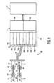
- Figure 1 illustrates a block diagram of one type of magnetic storage device 10 according to the invention, in this case a hard disk drive for mass storage of data.
- the device 10 includes a plurality of magnetic disks (of which only two (1A, 1B) are shown for purposes of clarity), and a plurality of pairs of write heads 2A1, 2A2; 2B1, 2B2 and read sensors 3A1, 3A2; 3B1, 3B2 mounted on respective servo controlled arms 4 which position the heads and sensors radially relative to corresponding sides of the spinning disks 1.
- the servo control of the arms and of the speed of the spinning disks is well known in the art and not pertinent to the present invention, but will be understood to include various servo motors, sensors and control circuits therefor.
- a preamplifier IC 5 includes a plurality of write channels 6A1, 6A2; 6B1, 6B2 and a plurality of read channels 7A1, 7A2; 7B1; 7B2, each write channel driving a respective write head to write information to a respective side of a disk 1A, 1B and each read channel driving a read sensor to read information from a respective side of a disk 1A, 1B.
- These write and read channels grouped conventionally in a pair wise configuration, form a part-per-head (or head interface) portion 5A of the preamplifier IC.
- the IC 5 is coupled to the read sensors and write heads via a flexible cable interconnect 8, which electrically connects the write heads and read sensors to the read and write channels through-connection pins/bumps 9 of the preamplifier IC 5.
- the IC 5 further includes a back-end read portion 5C and a front-end write portion 5B.
- the front-end read portions contain a first-gain stage for each read sensor, while the back-end read stage contains a plurality of gain stages and control circuitry common to all of the front-end read channels and is selectively coupled to a front-end read channel 7A1, 7A2, 7B1, 7B2 depending on which read sensor is selected to read information from a disk 1A, 1B.
- the preamplifier IC 5 in a hard disk drive is coupled to a further IC 11 which, for reading information, includes at least an equalizer and a bit detector.
- FIG. 2A is a graph which illustrates a voltage waveform of a typical disturbance caused by a write-to-read transition.
- the write-to-read transition occurs and the disturbance rapidly peaks to a peak P during time period A.
- the disturbance rapidly decays through zero volts at time B, to a negative peak ("-P") at a time C. Over a period of time (e.g. periods C-F,...
- the disturbance on the order of micro-seconds, the disturbance has a long tail and decays from the negative peak towards zero volts.
- the waveform of Fig. 2A is for illustration purposes only, and each combination of read sensor, write head, flexible interconnect and preamplifier IC will generate a proportionally different waveform.
- the present inventors have found that the waveforms for write-to-read disturbances in a high speed hard disk drive typically have a high initial peak, a negative peak and decay over time (e.g. periods A-F, ... n) with a long tail, and are measurable and characterizable through component testing.
- Figure 3A is a block diagram of a read channel 100 according to the invention having a plurality of gain stages, for example 3-5 stages, to amplify the signal from a read sensor 3 so that it can be decoded by a decoding circuit within the read/write channel IC.
- An MR read sensor 3 is coupled to an output buffer 130 via a plurality of gain stages 110, 115, 120 and 125 (Gm 1 , Gm n , Gm n+1 , Gm n+2 ) in the forward signal path 160 of the read channel 100.
- the gain stages 110, 115, 120 and 125 provide an amplified information signal via output buffer 130 to an equalizer 145 and a bit detector 150, which together form part of a decoder circuit, and which converts the analog information signal into a train of successive digital bits.
- the train of successive digital bits is then decoded according to an algorithm, depending on how the information was encoded when written to the magnetic medium.
- a filter 155 having a time-dependent gain characteristic is introduced in the forward signal path 60 of read channel 100.
- Figure 2B illustrates the function of the filter 155.
- the filter At an initial time period A in Fig. 2A corresponding to the peak period of the write-to-read transition, the filter has a relatively high LCF A (low gain) exemplified by the line "A". With increasing time, the LCF of the filter 155 is decreased in a fashion generally corresponding to the decay characteristic of the write-to-read disturbance, as illustrated by the time-wise shift (right-to-left in Fig. 2B) of the LCF of filter 155.
- the time-dependent filter will have a correspondingly increased gain (reduced attenuation) at a given frequency.
- the filter 155 will have an LCF (LCF n ) and a gain "n” selected to not adversely effect the proper reading of data from the magnetic medium by the read sensor.
- LCF LCF n
- the time starting with time “n” and thereafter is considered the “settled” state of the read channel when in the READ mode.
- the number of steps in the gain of the filter is for illustration purposes only, and may vary according to the needs of the application.
- the gain stage 110 is in the front-end portion of IC 5, and one such gain stage 110 is present for each read channel.
- the gain stages 115, 120, 125, filter 155 and output buffer 130 are in the back-end circuitry of IC 5 and are common to all of the read channels.
- the equalizer 145 and bit detector 150 are conventionally on a separate IC 11.
- the zero is introduced in the "back-end” circuits of the read channel to more effectively reduce offsets.
- back-end circuits is meant the gain stages closer to the buffer 130 than the initial gain stage 110. By placing the zero close to the output, there are no or only few subsequent stages to introduce offset, and conversely the zero reduces the offset of all the prior circuitry.
- the filter is shown connected to output buffer 130.
- the pole or zero is also referred to in terms of the frequency at which the transfer function is infinity or zero, respectively.
- the filter 155 in the forward path is embodied by a low pass filter (“LPF") 135 in a feedback path 165 around a unity gain stage 120 in the forward path, the unity gain stage being implemented as an-emitter-follower.
- the LPF 135 has a single (dominant) pole which can be varied from a fairly high frequency F1 to a lower frequency F2.
- This circuit when in closed loop configuration, introduces a zero in the forward path. The location of this zero is varied from a high frequency F A to a low frequency F n as a result of varying the frequency of the pole in the feedback path from a high frequency F1 to the lower frequency F2. Varying the location of the pole of LPF 155 varies the LCF of the zero created thereby in the forward path 160, in the manner illustrated in Fig. 2B.
- write-to-read transients are at a lower frequency than the signal frequency being read.
- the first peak portion (from point I to B) is at a frequency higher than the tail portion starting from point B to point n.
- This information about the nature of write-to-read disturbance frequencies is used to vary the LCF of the signal path in the present invention.
- the LCF should be higher than the frequency of pulse 1-P-B. After point B, to suppress the tail portion, the LCF can be smaller.
- a READ signal is switched ON to activate the read channel 100, for an initial small duration of time (of the order of 100ns) when the transients from the read front-end are very large (e.g. time period A in Fig. 2A)
- the effective zero in the forward path is kept at a high frequency F A .
- the effective LCF in the forward path is moved through lower frequencies F B , F C , F D generally corresponding to the times B, C, D in Fig. 2A.
- the LCF reaches frequency F n , where it is kept while the read channel is in the READ mode. This transition from F A through F n corrects the long tail of the write-to-read disturbance.
- the LCF of the effective filter 155 in the forward path is moved in such a manner that the there is maximum attenuation when the magnitude and frequency of the disturbance is high and lower attenuation when the amplitude and frequency of the disturbance is low.
- the end point of the LCF is such that it doesn't interfere with normal reading of data; i.e. the frequency of the LCF is much lower than the data frequency.
- the transfer function is equal to (A 120 /(1 + (A 120 )(A 165 )), where A 120 is the gain of stage 120 (unity) and A 165 is the combined gain of the LPF 135 and of the Gm stage 140.
- the combined gain of stages 135 and 140 is about 20 at LCF n , so the offset is reduced by a factor of 21.
- the output of the LPF 135 is a voltage signal.
- a differentiator Gm f feedback stage 140 is included in the feedback path 165 to convert the voltage output of LPF 135 to a current for feeding back to the forward path at the output of the prior gain stage (in this case stage 115).
- the feedback loop 165 is shown around the gain stage 120 instead of around the last gain stage 125.
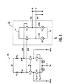
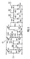
- FIG. 4a shows a circuit diagram of the gain stage 115 and the unity gain stage 120, which operates between an upper voltage supply rail VP and a lower voltage supply rail VN.
- the gain stage 115 includes cascode transistors Tc1, Tc2 coupled between load resistors RL1, RL2 and transconductance transistors T1n, T1p, respectively.
- the output signal currents from the Gm stage 140 are fed back to below the cascode transistors Tc1, Tc2 so that the Gm stage 140 does not capacitively load the forward path signal path.
- stage 115 is a transconductance stage (without considering load resistors Rl1/Rl2)
- the input signal voltage Vip, Vin from the prior gain stage(s), applied at the bases of the transistors T1n, T1p are converted to currents igp, ign by these devices.
- the currents Gpcp, Gpcn from the Gm stage 140 are subtracted therefrom, and applied across the load resistors RL1, RL2 to provide signal voltages gop, gon for the stage 120.
- Circuit branch 120a of stage 120 includes a first bipolar transistor T2n and a current source I3 biasing the emitter of the transistor T2n, and a circuit branch 120b with a current source 14 biasing the emitter of a second bipolar transistor T2n.
- the differential voltages gop and gon are applied to the bases of the transistors T2p, T2n.
- the outputs are differential voltages folp, foln which are fed to the LPF 135, as well as to the next gain stage 125. Since the stage 120 is an emitter-follower and functions as a unity gain buffer, the differential output voltages are approximately of the same magnitude as the differential input voltages for this stage.
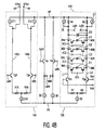
- FIG. 4b shows the circuit diagram for the time variant LPF 135 and the gm stage 140.
- the LPF also referred to as an integrator
- the inputs to the LPF are voltage signals foln, folp, which are the differential outputs from the stage (Gm n+1 ) 120.
- the signals foln, folp are coupled to the bases of bipolar transistors T3p, T3n.
- the emitter of each of the transistors T3p, T3n is coupled to a current source 15 via respective resistors R6, R7, the output of current source I5 being coupled to a lower voltage suppler rail VN.
- the collector of the transistor T3n is coupled via line L1 to the output of a current source 16 which is coupled in parallel with a load resistance R4.
- the collector of the transistor T3p is coupled via line L2 to a current source I7, also in parallel with a small load resistance R5.
- the purpose of the current sources I6, I7 is to effectively choose the operating point of nodes Ipfn, Ipfp (otherwise it would be (I5/2*RL). Coupled between the lines L1 and L2 are a plurality of capacitors C0, C1, C2, C3, and Cn with capacitor C0 being fixed and the remaining capacitances being controllable.
- the capacitors C1, C2, C3, and Cn are coupled, respectively, to the lines L1 and L2 via MOS devices M1A, M1B; M2A, M2B; M3A, M3B and MnA, MnB.
- the gates of the devices M1A, M1B receive a control voltage V1
- the gates of the devices M2A, M2B receive a control voltage V2
- the gates of the devices M3A, M3B receive a control voltage V3
- the control voltages are provided to selectively couple the capacitors C1 - Cn between lines L1 and L2 to vary the location of the pole of LPF 135.
- the outputs of the LPF 135 are differential voltages Lpfn, Lpfp.
- differential outputs are provided to a further emitter-follower buffer stage including current sources 18, 19 which bias respective bipolar transistors T4p, T4n.
- the differential outputs of this stage are signal voltages Lpfbn, Lpfbp.
- the feedback gm stage 140 includes a first branch 140a, and a second branch 140b.
- the first branch 140a includes a bipolar transistor T5p having a collector, a base coupled to receive the first differential input voltage Ipfbn, and an emitter biased by a current source I10.
- the second branch includes bipolar transistor T5n having a collector, a base coupled to receive the differential input voltage Ipfbp and an emitter biased by the current source I10.
- the emitters of the transistors T5p, T5n are coupled to the current source I10 via respective resistors R15, R16.
- a current sources I11 and a current source I12 are coupled, respectively, in the branches 140a, 140b between upper supply rail VP and the collectors of the transistor T2n, T2p.
- the outputs of the gm stage 140 are the currents Gpcp and Gpcn provided at outputs 43, 44, which are coupled to the prior amplifier stage 115 (Gm n ) in the forward signal path (as shown in Fig. 4A).
- the current source I10 provide a bias current to the emitters of the transistors T5n, T5p. Being a transconductance stage, the transistors T5n, T5p convert the differential small signal voltage Lpfbn, Lpfbp, into currents Gfcp, Gfcn which are proportional to the signal voltages Lpfbn, Lpfbp.
- the current sources I11, II2 replace the current drawn by the collectors of the transistors T5n, T5p so that the DC current at the outputs Gfcp, Gfcn is substantially zero, and therefor does not load and effect the operation of the prior gain stage 115.
- Fig. 5 shows one possible implementation of a circuit 170 which generates the control voltages VC1-VCn to drive the gate of the MOS switches in LPF 135, to achieve the time-dependent movement of the pole of the LPF 135 from the initial relatively high frequency F1 to the lower frequency F2.
- an R-C ladder structure is used to generate the control voltages in response to a READ control signal received at the input RdDEL.
- the outputs of the circuit 170 are the control voltages VC1, VC2, VC3 and VCn which control the MOS switches of the variable capacitor circuit of LPF 135 (Fig. 4B).
- the READ control signal received at input RdDEl drives the gates of a PMOS switch T672 and an NMOS switch T673, which together define a switchable current path 679 between supply rails VP, VN through a resistor R651.
- the current path 679 is coupled to drive the gates of a second pair of PMOS, NMOS transistors T674, T675 via resistor R652.
- the capacitor C660 and the resistor R651, and the capacitor C662 and the resistor 652 define a first RC time constant.
- the transistors T674, T675 have main current paths which define a second switchable current path 680 between rails VP, VN through serially coupled resistors R653, R654.
- the current path 680 is coupled to drive the gates of a third pair of PMOS, NMOS transistors T676, T677 which together similarly define a third switchable current path 681 through a resistor R655.
- the transistor T678 is coupled around the resistor R653.
- a control signal VC2DEL is applied to the gate of the transistor T678 to render it nonconductive, a second RC time constant is defined by the combination of the two resistors R653, R654 and the two capacitors C664, C665.
- a fourth time constant is defined by the combination of the resistor R654 and the two capacitors C663, C664 which is shorter than the third time constant.
- the third and fourth time constants define the time period between when the switches T674, T675 turn on and when the switches T676, T677 turn on.
- the combination of a fifth time constant defined by the RC pair of a resistor R655 and a capacitor C666 and of a sixth time constant defined by the RC pair of a resistor R656 and a capacitor C668 controls the time period between the turning on of the switches T676, T677 and the generation of the control voltage VC3.
- Subsequent time constants which define the time lapse between the generation of the control signal VC4 and VC3, and between VCn and VC4 are defined by the further RC pairs R657, C669; R658, C670; and R659, C671.
- the circuit 170 operates as follows. As illustrated in Fig. 6, when the input RdDEL transitions from a logic low to a logic high (corresponding to a write-to-read transition), the switch T672 turns off and the switch T673 begins to turn on when RdDel reaches the threshold voltage of switch T673, about 0.7 V. This couples the lower supply rail VN to generate the control signal VC2 controlled by the RC time constant of the resistors R651, R652 and capacitors C660 and C662.
- the signal VC1, as shown in Fig. 6 is initially high, due to the previous state of the signal RdDel being logic low. As this signal VC decreases, the NMOS switch T675 turns off and the PMOS switch T674 turns on.
- switch T677 turns on, the outputs VC2, VC3 through VCn are coupled to the rail VN, generating the control voltages VC2, VC3, VCn at these outputs with time delays based on the intervening time constants between the respective delay and the switch T677.
- the switch T678 serves as an adjustment switch to optionally change the time constants between the control signals VC1 and VC2, by switching creating a shunt around the resistor R653 with the control signal VC2del.
- control input signals INTPULSE, Rddel, and Rddel2 and control voltages VC1 to VC4 generated by circuit 170 and driving the MOS switches in LPF 35 would typically appear as shown in Fig. 6.
- the slow switching signals for the MOS switches of the variable capacitor of Fig. 4B can be generated in several other ways, which could be easily implemented by those of ordinary skill in the art in view of the example of Fig. 5 and the waveforms of Fig. 6.
- Figure 7 is an alternative embodiment of the variable capacitance circuit within LPF 135.
- a key requirement of a preamplifier circuit with respect to entering the steady read mode is the absence of DC transients above 20 mV.
- the steady read mode is defined as beginning upon the last occurrence of a differential DC transient above this level. Accordingly, it is important that the switching of the capacitors in the LPF not induce differential DC transients. The present inventors recognized that this could occur if the voltage on each node of a capacitor C2 - Cn in LPF 135 were different when that capacitor was switched into the circuit, as different voltages would cause the capacitor to discharge, rapidly creating transient currents.
- Figure 7 shows capacitors C0 - Cn and PMOS switches M1A - M1n, M1B-M1n corresponding to Fig. 4B. Additionally, Fig. 7 shows circuitry which equalizes the voltage on the nodes on either side of the capacitors C1- Cn prior to the capacitor being switched into the circuit.
- a transistor T81A is coupled in the branch L3 and has its emitter coupled to the collector of a diode connected transistor T82A.
- the base of the transistor T81A is coupled to branch L1, and is at the same potential as node Lpfn.
- the base of the transistor T82A is one diode drop below node Lpfn.
- Transistor T83A has its base coupled to the base of the transistor T82A and its emitter coupled to the rail VP via a current source I13.
- the node LpfmA, between the current source I13 and the emitter of the transistor T83A is one diode drop above the base of transistor T82A, so is at the same voltage as node Lpfn.
- the difference in base-emitter voltages due to different currents and mismatches in transistors is accounted for by appropriate dimensioning of the transistors T82A, T83A to achieve voltage equivalence between nodes Lpfn and LpfmA.
- the transistors T81B, T82B, T83B are coupled in a corresponding manner to the circuit branches L2, L4, L6, so that the node LpfmB is at the same potential as node Lpfp in branch L2.
- the control gate of PMOS equalization transistors M1C, M1D are coupled to the input RdDel and the control gate of PMOS transistors M1A, M1B are coupled to receive control voltage VC1 of Figure 5.
- the gates of PMOS equalization transistors M2C,M2D; M3C; M3D and MnC; MnD are coupled to receive the signal Rddel2 and the gates of the PMOS transistors M2A,M2B; M3A, M3B and MnA,MnB receive the control voltages VC2, VC3, VCn.
- the signal VC1 is initially high and the signals RdDel and Rddel2 are initially low.
- the equalization switches M1C-MnC and M1D-MnD are initially conductive and couple each of the capacitors C1 - Cn to the nodes LPFmA, Lpfmb. Both nodes are coupled to the same DC potential thereby.
- the nodes LpfmA, LpfmB are coupled to the nodes Lpfn, Lpfp through two emitter followers (formed by the transistors T81A, T82A; T82A, T82B) the capacitance of devices C1 - Cn is reduced by a factor of $ 2 and are substantially not reflected to the nodes Lpfn, Lpfp, so that the cut-off frequency of filter 135 is primarily determined by the capacitance of device C0.
- Rddel goes high, switches M1C and M1D turn off, as signal VC1 goes low and switches M1A, M1B turn on to bring capacitor C1 into circuit.
- Switches M1C-MnC and M1D-MnD introduce gate-source and gate-drain capacitances into the LPF 135, and thus may introduce their own current transients upon switching.
- a number of compensating PMOS transistors (M2An-MnAa; M1Cn-MnCn; M2Bn-MnBn; M1Dn-MnDn) are provided corresponding to respective ones of the PMOS switches M2A-MnA; M1C-MnC; M2B-MnB; M1D-MnD.
- the compensating PMOS transistors have their drains coupled to their sources, effectively doubling their capacitive effect and allowing these compensating devices to be substantially reduced in size.
- the compensating PMOS devices are provided with a charging signal at their gates, at the same time their respective equalizing PMOS switches are driven, which charging signal is selected to induce a charge therein of the opposite sense as the charge induced in the respective equalization switch when it is switched.
- the charging signals can be selected to reduce transient currents based on the actual transients induced in the IC by the equalization switches, whereas a fixed compensating capacitor could not.
- the compensating CMOS devices minimize transients and ensure that the equalization circuitry doesn't degrade its own performance with respect to reducing the settling time of write-to-read disturbances.
- the MOSFET switches T85, T86 receive signal INTON which controls whether the LPF 135 is on or off.
- the switch T4 receives a control signal INTGAIN, and switches the resistor R2 into and out of circuit with the resistor R1.
- the resistors R1, R2 determine the DC gain of LPF 135 and signal INTGAIN is used to switch the LPF 135 between a high and a low gain mode. This provides a different gain control mechanism than the variable capacitance circuitry, which varies the pole of the LPF.
- programmability of write-to-read settling time in the read channels is programmable. This will enable a user of the preamplifier IC to program the suppression characteristics in each preamplifier IC to fine tune variations in write-to-read disturbances in each hard disk drive, thereby optimizing performance.
- programmability is achieved through a serial interface connection with the preamplifier IC. Registers in the serial interface are designated to turn the "knobs" of various control elements in the read channel which control write-to-read suppression.
- FIG 8 is a block diagram of one embodiment illustrating the programming of a preamplifier IC through a user interface. Elements corresponding to those in previous Figures bear the same reference numbers.
- the read channel includes two programmable control elements which control the write-to-read suppression.
- the first control element is in the first gain stage 110 coupled to a read sensor 3.
- the second control element is a "back-end" control circuit W2RINT 180 corresponding to the LPF 135 and Gm stage 140 in combination with the control circuit 170 of Fig. 5. Both of these control elements are controlled by the contents of a serial interface register 205 of a serial interface 200.
- This serial interface register is an eight bit register storing the following variables (in the order of most-significant-bit (MSB) to least-significant-bit (LSB)): BCPW, IBFALL, IBPA, IBPW, W2RINTDEL2, W2RINTDEL1, W2RINTG and W2RINTON.
- MSB most-significant-bit
- LSB least-significant-bit
- the first gain stage 110 has cross coupled capacitors C115, C116 and a feedback amplifier ("FBA") 110e between the differential outputs 110c, 110d and the cross-coupled capacitors.
- FBA feedback amplifier
- This first gain stage 110 with cross-coupled capacitors is known, for example, from U.S. Patent 5,559,646 (Voorman et al), incorporated herein by reference.
- This gain stage 110 also includes a conventional common mode control circuit which controls the common mode DC voltage.
- Varying the gain of the feedback amplifier 1 10e controls the low comer frequency, in other words a zero, of the first stage 110.
- the feedback amplifier 110e is a transconductance (Gm)stage whose gain is controlled by a biasing current Ib supplied to it from a digital-to-analog converter ("DAC") 112.
- the current Ib is controlled by a control pulse IBPULSE supplied to DAC 112 by a pulse generation circuit 210. It is noted that it is known in the art to vary the current Ib to change the comer frequency of the first stage between two frequencies and to control the timing of the switchover with a controlled pulse signal. These function are present in Philips Semiconductors' TDA 5360 preamp circuit. However, the changeover is controlled internally, and no programmability through a user interface is available.
- the write-to-read circuit senses the onset of the write-to-read transition ("WRT") moment, which is graphically illustrated in chart 9A of Fig. 9.
- the write-to-read transition is known from a control signal in the magnetic storage apparatus which controls when the apparatus switches from the write mode to the read mode).
- the control pulse IBPULSE illustrated in chart 9B, is supplied by the pulse generation circuit 210. Three of the eight register bits control this bias current.
- the register bit IBPW is used to control the pulse width "PW”. (Chart 9B)
- the pulse width determines the duration of write-to-read suppression of the feedback amplifier 110e.
- the register bit IBPA controls the amplitude "PA” of the control pulse, which determines the amplitude of the bias current Ib, which in turn controls the location of the LCF of the gain stage 110 during write-to-read transition.
- the register bit IBFALL controls the fall time "FT" (slope) of the pulse IBPULSE to ensure a smooth transition so as not create an extra disturbance in the read channel. Depending on the register setting of IBPW, it generates a pulse width PW approximately 150ns to 300ns long.
- the register bit BCPW controls the common mode control circuit within stage 110 to further reduce DC transients at the write-to-read transition.
- the maximum low comer frequency (LCF) of the first stage 110 is programmed to be 2MHz to 5MHz.
- the LCF of the preamplifier IC is determined by the gain of the feedback transconductor in the first stage.
- the LCF is shifted to a higher frequency to filter out the write-to-read transient.
- this higher frequency of the LCF of the first stage 110 can be 6MHz to 10MHz.
- the LCF is shifted back to its lower programmed value so it will not adversely affect reading of the data signal.
- the back-end control circuit 180 is controlled by the register bits W2RINTDEL1, W2RINTON, W2RING, and W2RINTDEL2.
- Pulse generation circuit 210 generates a second pulse INTPULSE (Chart 9C) which is fed to W2RINT 180.
- Register bit W2RINTDEL1 controls the duration that the LCF of circuit 180 is at the first, relatively high frequency.
- Register bit W2RINTDEL1 directly controls the delay time of INTPULSE (from the READ signal to reachiong the logic threshold on INTPULSE.
- INTPULSE is input to control circuit 170 (Fig. 5) and therefore controls the delay between the write-to-read transition and the activation of switches TT672, T673.
- Register bit W2RINTON turns circuit 180 on and off, via the switches T85, T86 (Fig. 7)
- Register-bit W2RINTG controls the gain of the LPF 135, via switch T4.
- Register bit W2RINTDEL2 is provided to the input VC2Del, and thus controls the duration of change of the LCF from the first, relatively high frequency to the second, relatively low frequency.
- the first relatively high frequency may be 15MHz
- the second lower frequency may be 150 KHz.
- the LCF is initially at 15MHZ to suppress the high initial peak illustrated in Fig. 2A.
- the LCF is moved to 150 Khz gradually to suppress the long tail without over filtering, and is then maintained at 150 KHz. This very low LCF is to ensure that the existence of the feedback circuit 180 does not have a significant impact on the overall frequency response of the read channel.
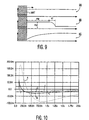
- Fig. 10 is a graph which illustrates the effect of the first stage 110 in reducing the write-to-read transition.
- Line “A” is an uncorrected write-to-read disturbance.
- Line “B” is the write-to-read disturbance with only the FBA 110e activated to reduce the disturbance.
- Line “C” shows the additional reduction provided by a boost in the gain of the common mode control circuit within stage 110 to reduce DC transients at this first stage.
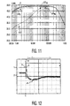
- Figure 11 illustrates the frequency response of the entire read channel 100 with the feedback integrator (stages 135, 140) in different gain modes.
- Line HG represents the high gain mode of the feedback integrator, which would occur if the W2RINTG bit is set to high.
- the LCF of the system, LCF HG in the high gain mode is dominated by the feedback integrator and is at a high frequency to filter the peak portion of the write-to-read disturbance.
- Line LG represents the integrator in a lower gain mode, when the W2RINTG bit is set to logic high.
- Line R represents the steady state of the read path frequency response during the read mode.
- Line O is the frequency response of the read channel when the feedback integrator is turned off.
- the integrator has little effect on the frequency response of the read channel. This is because the zero introduced by the W2RINT 180 when the read channel is nominally operating is sufficiently lower than (approx. 10 times lower freq.) than the zero of the first stage 110 of the preamplifier that the zero (i.e. the low comer frequency) of the overall read channel is not affected by the zero in the W2RINT 180.
- the integrator nonetheless significantly reduces the offset of the preamplifier IC.
- Figure 12 illustrates an actual write-to-read disturbance after filtering with a preamplifier IC having both of the first and second control elements.
- the write-to-read transition is at momet "I" in the Fig.
- the disturbance has a high initial peak "P", of a negative peak "-P", and a tail.
- the beginning of the settled read mode is defined as beginning at the last occurrence where the disturbance has a magnitude of 20 mV. In Fig. 12, this occurs at a time of 124 Ns, at point "C".
- settling time was typically on the order of 4 to 10 microseconds.
- the present invention provides an improvement in settling time averaging on the order of a factor of 50.
Landscapes
- Engineering & Computer Science (AREA)
- Power Engineering (AREA)
- Signal Processing (AREA)
- Digital Magnetic Recording (AREA)
- Signal Processing For Digital Recording And Reproducing (AREA)
- Electronic Switches (AREA)
Applications Claiming Priority (3)
| Application Number | Priority Date | Filing Date | Title |
|---|---|---|---|
| US09/407,776 US6404578B1 (en) | 1999-09-28 | 1999-09-28 | Circuit for reduction and optimization of write-to-read settling times in magnetic medium storage devices |
| US407776 | 1999-09-28 | ||
| PCT/EP2000/009400 WO2001024168A1 (en) | 1999-09-28 | 2000-09-25 | Circuit for reduction and optimization of write-to-read settling times in magnetic medium storage devices |
Publications (2)
| Publication Number | Publication Date |
|---|---|
| EP1135769A1 EP1135769A1 (en) | 2001-09-26 |
| EP1135769B1 true EP1135769B1 (en) | 2004-12-01 |
Family
ID=23613481
Family Applications (1)
| Application Number | Title | Priority Date | Filing Date |
|---|---|---|---|
| EP00967792A Revoked EP1135769B1 (en) | 1999-09-28 | 2000-09-25 | Circuit for reduction and optimization of write-to-read settling times in magnetic medium storage devices |
Country Status (6)
| Country | Link |
|---|---|
| US (2) | US6404578B1 (enExample) |
| EP (1) | EP1135769B1 (enExample) |
| JP (1) | JP2003510747A (enExample) |
| KR (2) | KR20010080576A (enExample) |
| DE (1) | DE60016374T2 (enExample) |
| WO (1) | WO2001024168A1 (enExample) |
Families Citing this family (30)
| Publication number | Priority date | Publication date | Assignee | Title |
|---|---|---|---|---|
| US6567228B1 (en) * | 2000-06-03 | 2003-05-20 | Koninklijke Philips Electronics N.V. | Optimized stage reader for low cost implementation of preamplifiers |
| US6751034B1 (en) * | 2000-07-19 | 2004-06-15 | Texas Instruments Incorporated | Preamplifier read recovery parade |
| US6721117B2 (en) * | 2000-11-29 | 2004-04-13 | Agere Systems Inc. | Read/write system with reduced write-to-read transition recovery time independent from input voltage and input current offset |
| WO2002060055A1 (en) * | 2001-01-24 | 2002-08-01 | Koninklijke Philips Electronics N.V. | Tunable integrated rf filter having switched field effect capacitors |
| US7292400B2 (en) * | 2001-04-23 | 2007-11-06 | Seagate Technology Llc | Device for limiting current in a sensor |
| US6876253B2 (en) | 2001-09-28 | 2005-04-05 | Koninklijke Philips Electronics N.V. | Amplifier for alternating signals superimposed on a continuous signal and method for amplifying such signals |
| FR2850499B1 (fr) * | 2003-01-28 | 2005-10-21 | St Microelectronics Sa | Procede et circuit de correction de l'offset d'une chaine d'amplification |
| US7339760B2 (en) * | 2004-01-30 | 2008-03-04 | Agere Systems Inc. | Integrated bias and offset recovery amplifier |
| US7119977B2 (en) * | 2004-04-17 | 2006-10-10 | Agere Systems Inc. | Reduced recovery time for perpendicular recording systems |
| US20070127149A1 (en) * | 2005-12-02 | 2007-06-07 | Texas Instruments Incorporated | Offset cancellation scheme for perpendicular reader |
| US8144125B2 (en) | 2006-03-30 | 2012-03-27 | Cypress Semiconductor Corporation | Apparatus and method for reducing average scan rate to detect a conductive object on a sensing device |
| US8547114B2 (en) | 2006-11-14 | 2013-10-01 | Cypress Semiconductor Corporation | Capacitance to code converter with sigma-delta modulator |
| US8089288B1 (en) | 2006-11-16 | 2012-01-03 | Cypress Semiconductor Corporation | Charge accumulation capacitance sensor with linear transfer characteristic |
| US8144126B2 (en) | 2007-05-07 | 2012-03-27 | Cypress Semiconductor Corporation | Reducing sleep current in a capacitance sensing system |
| US8436263B2 (en) * | 2007-06-29 | 2013-05-07 | Cypress Semiconductor Corporation | Noise resistant capacitive sensor |
| US8089289B1 (en) | 2007-07-03 | 2012-01-03 | Cypress Semiconductor Corporation | Capacitive field sensor with sigma-delta modulator |
| US8169238B1 (en) * | 2007-07-03 | 2012-05-01 | Cypress Semiconductor Corporation | Capacitance to frequency converter |
| US8570053B1 (en) | 2007-07-03 | 2013-10-29 | Cypress Semiconductor Corporation | Capacitive field sensor with sigma-delta modulator |
| US8525798B2 (en) | 2008-01-28 | 2013-09-03 | Cypress Semiconductor Corporation | Touch sensing |
| US8358142B2 (en) | 2008-02-27 | 2013-01-22 | Cypress Semiconductor Corporation | Methods and circuits for measuring mutual and self capacitance |
| US8319505B1 (en) | 2008-10-24 | 2012-11-27 | Cypress Semiconductor Corporation | Methods and circuits for measuring mutual and self capacitance |
| US9104273B1 (en) | 2008-02-29 | 2015-08-11 | Cypress Semiconductor Corporation | Multi-touch sensing method |
| US8321174B1 (en) | 2008-09-26 | 2012-11-27 | Cypress Semiconductor Corporation | System and method to measure capacitance of capacitive sensor array |
| US8723827B2 (en) | 2009-07-28 | 2014-05-13 | Cypress Semiconductor Corporation | Predictive touch surface scanning |
| US8711502B1 (en) | 2012-10-12 | 2014-04-29 | Lsi Corporation | Preamplifier-to-channel communication in a storage device |
| TWI530090B (zh) * | 2013-10-02 | 2016-04-11 | 聯詠科技股份有限公司 | 放大器電路及其操作方法 |
| WO2015051535A1 (en) | 2013-10-11 | 2015-04-16 | Motorola Solutions, Inc. | Interference detection and mitigation in radio frequency receivers |
| EP3477895B1 (en) * | 2017-10-26 | 2020-05-06 | Melexis Technologies NV | A transceiver unit for transmitting data via a differential bus |
| US10896694B2 (en) * | 2018-10-30 | 2021-01-19 | Marvell Asia Pte, Ltd. | Thermal compensation for laser in heat assisted magnetic recording |
| US11716097B2 (en) | 2021-12-29 | 2023-08-01 | Western Digital Technologies, Inc. | Signal correction using soft information in a data channel |
Family Cites Families (24)
| Publication number | Priority date | Publication date | Assignee | Title |
|---|---|---|---|---|
| US3697985A (en) * | 1970-09-23 | 1972-10-10 | Bendix Corp | Rear end warning system for automobiles |
| US4185246A (en) | 1978-02-27 | 1980-01-22 | Schlumberger Technology Corporation | Circuit for reducing transients by precharging capacitors |
| JPS572137A (en) | 1980-06-04 | 1982-01-07 | Mitsubishi Electric Corp | Automatic line equalizing device |
| GB2165117B (en) * | 1984-09-29 | 1987-12-31 | Standard Telephones Cables Plc | Optical receiver |
| US4914398A (en) * | 1988-08-01 | 1990-04-03 | International Business Machines Corporation | Method and circuitry to suppress additive disturbances in data channels containing MR sensors |
| US5220220A (en) | 1989-09-20 | 1993-06-15 | Gennum Corporation | Noise suppression system |
| US5270875A (en) * | 1990-11-13 | 1993-12-14 | Colorado Memory Systems, Inc. | Programmable filter/equalizer for duel speed and density magnetic recording devices |
| JPH05166111A (ja) | 1991-12-16 | 1993-07-02 | Nec Ibaraki Ltd | 磁気ディスク装置 |
| US5309112A (en) | 1992-07-16 | 1994-05-03 | Motorola, Inc. | Switched-capacitor circuit power down technique |
| US5373294A (en) | 1993-07-12 | 1994-12-13 | Nec Electronics, Inc. | Current switch for a high speed DAC |
| DE69428678T2 (de) | 1993-10-06 | 2002-07-11 | Koninklijke Philips Electronics N.V., Eindhoven | Vorrichtung zum auslesen von informationen von einer spur eines aufzeichnungsträgers |
| KR950704695A (ko) | 1993-10-06 | 1995-11-20 | 프레데릭 얀 스미트 | 자기 기록 캐리어로부터 정보 신호를 판독하는 장치(Arrangement for reading information from a track on a record carrier comprising a fast settling read amplifier for magneto-resistive heads) |
| US5648738A (en) * | 1994-11-01 | 1997-07-15 | Cirrus Logic, Inc. | Read channel having auto-zeroing and offset compensation, and power-down between servo fields |
| US6172548B1 (en) | 1994-12-30 | 2001-01-09 | Stmicroelectronics, Inc. | Input stage with reduced transient time for use in multiplexing transducers that require a switched DC bias |
| JPH0944810A (ja) * | 1995-07-24 | 1997-02-14 | Mitsubishi Electric Corp | Mrヘッド用信号再生回路 |
| WO1997015115A1 (en) | 1995-10-20 | 1997-04-24 | Philips Electronics N.V. | Differential switched capacitor filtering |
| JPH09148886A (ja) | 1995-11-27 | 1997-06-06 | Fujitsu Ten Ltd | 信号処理回路 |
| JP3458567B2 (ja) * | 1995-11-28 | 2003-10-20 | 三菱電機株式会社 | Mrヘッド用増幅器 |
| US5933038A (en) | 1997-02-25 | 1999-08-03 | Sun Microsystems, Inc. | Flip-flop with logic function incorporated therein with minimal time penalty |
| US5841310A (en) | 1997-04-08 | 1998-11-24 | Burr-Brown Corporation | Current-to-voltage integrator for analog-to-digital converter, and method |
| US5943290A (en) | 1998-06-12 | 1999-08-24 | Oak Technology, Inc. | Apparatus for providing a quiet time before analog signal sampling in a mixed signal integrated circuit employing synchronous and asynchronous clocking |
| US6147523A (en) * | 1998-06-22 | 2000-11-14 | National Semiconductor Corporation | Overshoot control and damping circuit for high speed drivers |
| US6091616A (en) * | 1998-10-21 | 2000-07-18 | Lucent Technologies Inc. | Drive compensation circuit for synchronous rectifier and method of operating the same |
| US6252459B1 (en) * | 1999-03-30 | 2001-06-26 | Siemens Microelectronics, Inc. | System and method for a dual bandwidth capacitor multiplying filter |
-
1999
- 1999-09-28 US US09/407,776 patent/US6404578B1/en not_active Expired - Fee Related
- 1999-12-22 US US09/469,873 patent/US6400217B1/en not_active Expired - Fee Related
-
2000
- 2000-09-21 KR KR1020017006556A patent/KR20010080576A/ko not_active Withdrawn
- 2000-09-25 JP JP2001527273A patent/JP2003510747A/ja not_active Withdrawn
- 2000-09-25 KR KR1020017006593A patent/KR20010080588A/ko not_active Withdrawn
- 2000-09-25 DE DE60016374T patent/DE60016374T2/de not_active Expired - Lifetime
- 2000-09-25 EP EP00967792A patent/EP1135769B1/en not_active Revoked
- 2000-09-25 WO PCT/EP2000/009400 patent/WO2001024168A1/en not_active Ceased
Also Published As
| Publication number | Publication date |
|---|---|
| US6404578B1 (en) | 2002-06-11 |
| KR20010080588A (ko) | 2001-08-22 |
| KR20010080576A (ko) | 2001-08-22 |
| JP2003510747A (ja) | 2003-03-18 |
| DE60016374D1 (de) | 2005-01-05 |
| DE60016374T2 (de) | 2005-12-01 |
| WO2001024168A1 (en) | 2001-04-05 |
| US6400217B1 (en) | 2002-06-04 |
| EP1135769A1 (en) | 2001-09-26 |
Similar Documents
| Publication | Publication Date | Title |
|---|---|---|
| EP1135769B1 (en) | Circuit for reduction and optimization of write-to-read settling times in magnetic medium storage devices | |
| US6424480B1 (en) | Magnetic medium storage apparatus with read channel having a programmable write-to-read suppression | |
| EP0805436B1 (en) | Reproducing circuit for a magnetic head | |
| US6552593B2 (en) | Active auto zero circuit for programmable time continuous open loop amplifiers | |
| US20050218853A1 (en) | Motor drive semiconductor integrated circuit and magnetic disk storage apparatus | |
| EP1399919B1 (en) | Write output driver with internal programmable pull-up resistors | |
| JP3257886B2 (ja) | 磁気抵抗効果型ヘッド用信号再生回路 | |
| US6167010A (en) | Disk reproduction apparatus and tracking servo circuit | |
| US7242545B1 (en) | Asymmetric compensation circuit | |
| JPH0430650B2 (enExample) | ||
| US20020176186A1 (en) | Efficient analog front end for a read/write channel of a hard disk drive running from a highly regulated power supply | |
| US6046875A (en) | Linear transconductance circuit having a large linear range | |
| KR100717911B1 (ko) | 판독 채널을 구비하는 장치 및 집적 회로 | |
| JPS6246406A (ja) | アナログ読取り信号の処理回路装置 | |
| US6549357B1 (en) | Selectable input pole compensation for a disk drive read head | |
| KR100192597B1 (ko) | 하드디스크 드라이버 장치의 증폭회로 | |
| JP2954795B2 (ja) | 信号処理回路 | |
| JPS59231777A (ja) | トラツク間検出装置 | |
| JPH0757395A (ja) | 再生装置 | |
| JPH11328926A (ja) | 磁気記録再生装置 | |
| JP2003510940A (ja) | 過渡障害を低減する荷電平衡方式フィルタを有する集積回路 | |
| WO2003003568A2 (en) | Active auto zero circuit for programmable time continuous open loop amplifiers | |
| JPH1196702A (ja) | 磁気ディスク装置及び該装置に用いるサーマルアスペリティー制御方法 | |
| JP2001338401A (ja) | 磁気ディスク装置及び磁気ディスクシステム |
Legal Events
| Date | Code | Title | Description |
|---|---|---|---|
| PUAI | Public reference made under article 153(3) epc to a published international application that has entered the european phase |
Free format text: ORIGINAL CODE: 0009012 |
|
| AK | Designated contracting states |
Kind code of ref document: A1 Designated state(s): AT BE CH CY DE DK ES FI FR GB GR IE IT LI LU MC NL PT SE |
|
| 17P | Request for examination filed |
Effective date: 20011005 |
|
| 17Q | First examination report despatched |
Effective date: 20020208 |
|
| GRAP | Despatch of communication of intention to grant a patent |
Free format text: ORIGINAL CODE: EPIDOSNIGR1 |
|
| GRAS | Grant fee paid |
Free format text: ORIGINAL CODE: EPIDOSNIGR3 |
|
| GRAA | (expected) grant |
Free format text: ORIGINAL CODE: 0009210 |
|
| AK | Designated contracting states |
Kind code of ref document: B1 Designated state(s): DE FR GB NL |
|
| PG25 | Lapsed in a contracting state [announced via postgrant information from national office to epo] |
Ref country code: NL Free format text: LAPSE BECAUSE OF FAILURE TO SUBMIT A TRANSLATION OF THE DESCRIPTION OR TO PAY THE FEE WITHIN THE PRESCRIBED TIME-LIMIT Effective date: 20041201 |
|
| REG | Reference to a national code |
Ref country code: GB Ref legal event code: FG4D |
|
| REG | Reference to a national code |
Ref country code: IE Ref legal event code: FG4D |
|
| REF | Corresponds to: |
Ref document number: 60016374 Country of ref document: DE Date of ref document: 20050105 Kind code of ref document: P |
|
| NLV1 | Nl: lapsed or annulled due to failure to fulfill the requirements of art. 29p and 29m of the patents act | ||
| REG | Reference to a national code |
Ref country code: GB Ref legal event code: 746 Effective date: 20050518 |
|
| PLBE | No opposition filed within time limit |
Free format text: ORIGINAL CODE: 0009261 |
|
| ET | Fr: translation filed | ||
| 26N | No opposition filed |
Effective date: 20050902 |
|
| REG | Reference to a national code |
Ref country code: FR Ref legal event code: D6 |
|
| PLBR | Kind of request for revocation recorded |
Free format text: ORIGINAL CODE: EPIDOSNRVR2 |
|
| PLBT | Request for revocation filed by patent holder |
Free format text: ORIGINAL CODE: EPIDOSNRVR1 |
|
| PLDC | Decision to revoke patent |
Free format text: ORIGINAL CODE: 0009219 |
|
| PLDH | Decision on request for revocation |
Free format text: ORIGINAL CODE: EPIDOSNRVR3 |
|
| RDAA | Patent revoked on request of proprietor |
Free format text: ORIGINAL CODE: 0009220 |
|
| STAA | Information on the status of an ep patent application or granted ep patent |
Free format text: STATUS: PATENT REVOKED BY PROPRIETOR |
|
| PGFP | Annual fee paid to national office [announced via postgrant information from national office to epo] |
Ref country code: DE Payment date: 20081112 Year of fee payment: 9 |
|
| PGFP | Annual fee paid to national office [announced via postgrant information from national office to epo] |
Ref country code: FR Payment date: 20080926 Year of fee payment: 9 |
|
| REG | Reference to a national code |
Ref country code: FR Ref legal event code: ST Effective date: 20100531 |
|
| PGFP | Annual fee paid to national office [announced via postgrant information from national office to epo] |
Ref country code: GB Payment date: 20100930 Year of fee payment: 11 |
|
| GBPC | Gb: european patent ceased through non-payment of renewal fee |
Effective date: 20110925 |