EP1132957A2 - Verfahren zur Herstellung einer Leiterstruktur für einen integrierten Schaltkreis - Google Patents
Verfahren zur Herstellung einer Leiterstruktur für einen integrierten Schaltkreis Download PDFInfo
- Publication number
- EP1132957A2 EP1132957A2 EP01103715A EP01103715A EP1132957A2 EP 1132957 A2 EP1132957 A2 EP 1132957A2 EP 01103715 A EP01103715 A EP 01103715A EP 01103715 A EP01103715 A EP 01103715A EP 1132957 A2 EP1132957 A2 EP 1132957A2
- Authority
- EP
- European Patent Office
- Prior art keywords
- layer
- hard mask
- conductive material
- passivation layer
- passivation
- Prior art date
- Legal status (The legal status is an assumption and is not a legal conclusion. Google has not performed a legal analysis and makes no representation as to the accuracy of the status listed.)
- Granted
Links
Images


Classifications
-
- H—ELECTRICITY
- H10—SEMICONDUCTOR DEVICES; ELECTRIC SOLID-STATE DEVICES NOT OTHERWISE PROVIDED FOR
- H10W—GENERIC PACKAGES, INTERCONNECTIONS, CONNECTORS OR OTHER CONSTRUCTIONAL DETAILS OF DEVICES COVERED BY CLASS H10
- H10W20/00—Interconnections in chips, wafers or substrates
- H10W20/01—Manufacture or treatment
- H10W20/031—Manufacture or treatment of conductive parts of the interconnections
- H10W20/032—Manufacture or treatment of conductive parts of the interconnections of conductive barrier, adhesion or liner layers
- H10W20/038—Manufacture or treatment of conductive parts of the interconnections of conductive barrier, adhesion or liner layers covering conductive structures
- H10W20/039—Manufacture or treatment of conductive parts of the interconnections of conductive barrier, adhesion or liner layers covering conductive structures also covering sidewalls of the conductive structures
-
- H—ELECTRICITY
- H10—SEMICONDUCTOR DEVICES; ELECTRIC SOLID-STATE DEVICES NOT OTHERWISE PROVIDED FOR
- H10W—GENERIC PACKAGES, INTERCONNECTIONS, CONNECTORS OR OTHER CONSTRUCTIONAL DETAILS OF DEVICES COVERED BY CLASS H10
- H10W20/00—Interconnections in chips, wafers or substrates
- H10W20/01—Manufacture or treatment
- H10W20/031—Manufacture or treatment of conductive parts of the interconnections
- H10W20/032—Manufacture or treatment of conductive parts of the interconnections of conductive barrier, adhesion or liner layers
- H10W20/033—Manufacture or treatment of conductive parts of the interconnections of conductive barrier, adhesion or liner layers in openings in dielectrics
-
- H—ELECTRICITY
- H10—SEMICONDUCTOR DEVICES; ELECTRIC SOLID-STATE DEVICES NOT OTHERWISE PROVIDED FOR
- H10W—GENERIC PACKAGES, INTERCONNECTIONS, CONNECTORS OR OTHER CONSTRUCTIONAL DETAILS OF DEVICES COVERED BY CLASS H10
- H10W20/00—Interconnections in chips, wafers or substrates
- H10W20/01—Manufacture or treatment
- H10W20/031—Manufacture or treatment of conductive parts of the interconnections
- H10W20/032—Manufacture or treatment of conductive parts of the interconnections of conductive barrier, adhesion or liner layers
- H10W20/052—Manufacture or treatment of conductive parts of the interconnections of conductive barrier, adhesion or liner layers by treatments not introducing additional elements therein
- H10W20/0523—Manufacture or treatment of conductive parts of the interconnections of conductive barrier, adhesion or liner layers by treatments not introducing additional elements therein by irradiating with ultraviolet or particle radiation
-
- H—ELECTRICITY
- H10—SEMICONDUCTOR DEVICES; ELECTRIC SOLID-STATE DEVICES NOT OTHERWISE PROVIDED FOR
- H10W—GENERIC PACKAGES, INTERCONNECTIONS, CONNECTORS OR OTHER CONSTRUCTIONAL DETAILS OF DEVICES COVERED BY CLASS H10
- H10W20/00—Interconnections in chips, wafers or substrates
- H10W20/01—Manufacture or treatment
- H10W20/031—Manufacture or treatment of conductive parts of the interconnections
- H10W20/032—Manufacture or treatment of conductive parts of the interconnections of conductive barrier, adhesion or liner layers
- H10W20/054—Manufacture or treatment of conductive parts of the interconnections of conductive barrier, adhesion or liner layers by selectively removing parts thereof
-
- H—ELECTRICITY
- H10—SEMICONDUCTOR DEVICES; ELECTRIC SOLID-STATE DEVICES NOT OTHERWISE PROVIDED FOR
- H10W—GENERIC PACKAGES, INTERCONNECTIONS, CONNECTORS OR OTHER CONSTRUCTIONAL DETAILS OF DEVICES COVERED BY CLASS H10
- H10W20/00—Interconnections in chips, wafers or substrates
- H10W20/01—Manufacture or treatment
- H10W20/031—Manufacture or treatment of conductive parts of the interconnections
- H10W20/063—Manufacture or treatment of conductive parts of the interconnections by forming conductive members before forming protective insulating material
-
- H—ELECTRICITY
- H10—SEMICONDUCTOR DEVICES; ELECTRIC SOLID-STATE DEVICES NOT OTHERWISE PROVIDED FOR
- H10W—GENERIC PACKAGES, INTERCONNECTIONS, CONNECTORS OR OTHER CONSTRUCTIONAL DETAILS OF DEVICES COVERED BY CLASS H10
- H10W20/00—Interconnections in chips, wafers or substrates
- H10W20/01—Manufacture or treatment
- H10W20/031—Manufacture or treatment of conductive parts of the interconnections
- H10W20/063—Manufacture or treatment of conductive parts of the interconnections by forming conductive members before forming protective insulating material
- H10W20/0633—Manufacture or treatment of conductive parts of the interconnections by forming conductive members before forming protective insulating material using subtractive patterning of the conductive members
-
- H—ELECTRICITY
- H10—SEMICONDUCTOR DEVICES; ELECTRIC SOLID-STATE DEVICES NOT OTHERWISE PROVIDED FOR
- H10W—GENERIC PACKAGES, INTERCONNECTIONS, CONNECTORS OR OTHER CONSTRUCTIONAL DETAILS OF DEVICES COVERED BY CLASS H10
- H10W20/00—Interconnections in chips, wafers or substrates
- H10W20/01—Manufacture or treatment
- H10W20/071—Manufacture or treatment of dielectric parts thereof
-
- H—ELECTRICITY
- H10—SEMICONDUCTOR DEVICES; ELECTRIC SOLID-STATE DEVICES NOT OTHERWISE PROVIDED FOR
- H10W—GENERIC PACKAGES, INTERCONNECTIONS, CONNECTORS OR OTHER CONSTRUCTIONAL DETAILS OF DEVICES COVERED BY CLASS H10
- H10W20/00—Interconnections in chips, wafers or substrates
- H10W20/01—Manufacture or treatment
- H10W20/071—Manufacture or treatment of dielectric parts thereof
- H10W20/074—Manufacture or treatment of dielectric parts thereof of dielectric parts comprising thin functional dielectric layers, e.g. dielectric etch-stop, barrier, capping or liner layers
-
- H—ELECTRICITY
- H10—SEMICONDUCTOR DEVICES; ELECTRIC SOLID-STATE DEVICES NOT OTHERWISE PROVIDED FOR
- H10W—GENERIC PACKAGES, INTERCONNECTIONS, CONNECTORS OR OTHER CONSTRUCTIONAL DETAILS OF DEVICES COVERED BY CLASS H10
- H10W20/00—Interconnections in chips, wafers or substrates
- H10W20/01—Manufacture or treatment
- H10W20/071—Manufacture or treatment of dielectric parts thereof
- H10W20/074—Manufacture or treatment of dielectric parts thereof of dielectric parts comprising thin functional dielectric layers, e.g. dielectric etch-stop, barrier, capping or liner layers
- H10W20/077—Manufacture or treatment of dielectric parts thereof of dielectric parts comprising thin functional dielectric layers, e.g. dielectric etch-stop, barrier, capping or liner layers on sidewalls or on top surfaces of conductors
-
- H—ELECTRICITY
- H10—SEMICONDUCTOR DEVICES; ELECTRIC SOLID-STATE DEVICES NOT OTHERWISE PROVIDED FOR
- H10P—GENERIC PROCESSES OR APPARATUS FOR THE MANUFACTURE OR TREATMENT OF DEVICES COVERED BY CLASS H10
- H10P50/00—Etching of wafers, substrates or parts of devices
- H10P50/20—Dry etching; Plasma etching; Reactive-ion etching
- H10P50/26—Dry etching; Plasma etching; Reactive-ion etching of conductive or resistive materials
- H10P50/264—Dry etching; Plasma etching; Reactive-ion etching of conductive or resistive materials by chemical means
- H10P50/266—Dry etching; Plasma etching; Reactive-ion etching of conductive or resistive materials by chemical means by vapour etching only
- H10P50/267—Dry etching; Plasma etching; Reactive-ion etching of conductive or resistive materials by chemical means by vapour etching only using plasmas
-
- H—ELECTRICITY
- H10—SEMICONDUCTOR DEVICES; ELECTRIC SOLID-STATE DEVICES NOT OTHERWISE PROVIDED FOR
- H10P—GENERIC PROCESSES OR APPARATUS FOR THE MANUFACTURE OR TREATMENT OF DEVICES COVERED BY CLASS H10
- H10P50/00—Etching of wafers, substrates or parts of devices
- H10P50/71—Etching of wafers, substrates or parts of devices using masks for conductive or resistive materials
Definitions
- the invention relates to a method for producing a Conductor structure for an integrated circuit.
- the structures such integrated circuits move in the sub-micron range.
- Integrated circuits have a microelectronic applied to a common carrier (substrate) Circuit with a variety of components on.
- the degree of integration, a measure of the number of electronic Components on the chip can be obtained from VLSI (very large scale integration), ULSI (ultra large scale integration) or lie higher.
- metal level is realized with copper, there is a risk of corrosion when structuring the copper. This arises from the fact that after the etching of the copper Residues of the etching material on the exposed copper surfaces attack.
- Another disadvantage is that in chemical etching, copper is only removed at temperatures where the photoresist flows or even burns.
- a plasma etching method is known from the prior art US 4,026,742 known for the production of an integrated circuit.
- the problem also exists there when liquid etching solutions that the etching mask, which consists of a photoresistive material is made, disappears or peels off during etching so that a precise Structuring is difficult.
- the prior art US 4,026,742 is proposed to solve this problem
- Manufacture of the integrated circuit in the reaction chamber a gas having a halogen component in one Plasma state with a high frequency electromagnetic Field to use.
- the halogenated metal areas are by sublimation, evaporation or washing with water or removed another suitable solution.
- the plasma can be in a reaction chamber with a high frequency electromagnetic Field are generated.
- the procedure is for Generation of the desired structure of the metal for electrodes or lines on the semiconductor substrate or other microelectric Carriers. It is used in particular for the etching of Tungsten or molybdenum metal structures are used.
- the halogenated Gas essentially contains dichlorodifluoromethane.
- the current source works with a current of 180 mA at 1200 V and a frequency of 13.56 MHz. Because the plasma at more than 10,000 ° Celsius, the chamber material be designed accordingly to the reactions taking place to be able to resist. These are disadvantageously special To place requirements on the reaction chamber.
- connection channels Another method is known from the prior art US Pat. No. 5,817,572 for making connections between connection channels known.
- the dual damascene is also used in this publication Process described.
- a dielectric layer will deposited and by means of a two-stage etching process structured. In the first stage of the etching process, the most of the dielectric layer within the contact openings etched away. In the second step, the connection channels and the rest of the dielectric layer within the Contact openings etched away.
- the depth of the connection channels is difficult because of film deposition and uneven etching to control. The depth of the connection channels can be in the center of the wafer is too large and too small at the edge of the wafer. This results in large differences in the connection resistances on the same wafer.
- the metal deposition is difficult because the contact openings have an aspect ratio (Ratio of height to width) of 2: 1, 3: 1 or more can.
- the large aspect ratios make a sputter separation almost impossible.
- a layer of metal can pass through chemical vapor deposition within the contact openings and of the connection channels are separated.
- connection materials like aluminum, copper, gold and silver more typical Not deposited with chemical vapor deposition.
- polysilicon and tungsten can be mixed with chemical vapor deposition. This is the dual damascene Process for producing the desired conductor structure not very suitable for an integrated circuit.
- An object of the invention is to provide a method for manufacturing a conductor structure for an integrated circuit specify where the passivation of the metal layer is easy and is possible with just a few process steps. Farther should be those shown in the above prior art Disadvantages are avoided.
- the method according to the invention for producing a conductor structure for an integrated circuit has a structured first insulating layer on which a first passivation layer is applied. On the first passivation layer a layer of conductive material is applied, on which in turn a second passivation layer is applied. A hard mask is applied to this. Then the layer of conductive material in the areas provided by the hard mask.
- the first Passivation layer is provided in the hard mask Areas removed by sputtering and on the side wall of the conductive material at least in part again deposited.
- the layer of conductive material can be removed by reactive Ion etching take place.
- the layer of conductive material can also be removed by Sputtering done.
- the layer of conductive material advantageously has copper on. Copper has a relatively low ohmic resistance.
- the layer thickness of the conductive material is between 300 nm and 500nm.
- the passivation layers can be tantalum, tantalum nitride or have both.
- the first insulating layer advantageously has a silicon oxide or a material with a dielectric constant, which is lower than that of silicon oxide.
- the hard mask can be silicon nitride, silicon oxynitride or silicon oxide exhibit.
- the thickness of the hard mask is advantageously between 100 nm and 300 nm.
- the thickness of the first and the second is advantageously Passivation layer approx. 20 nm each.
- the surface can be covered with a third passivation layer be provided.
- the surface can also be covered with a second layer of insulation be provided.
- the surface is provided with a second insulating layer, it is then to be chemically and mechanically polished.
- the wafer is advantageously cooled during sputtering.
- the structured first insulating layer can be reactive Ion etching can be generated.
- the structuring of the layer of conductive material can be done by heating the wafer and then reactive ion etching respectively.
- the hard mask can be created by first Hard mask material deposited using chemical vapor deposition becomes. Then an anti-reflective layer is applied, over which a photoresist mask is applied. The Hard mask material is then attached to the through the photoresist mask designated areas etched off. Finally, the anti-reflective coating as well as the photoresist mask removed.
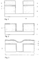
- the layer structure is shown in cross section, wherein a first insulating layer 2 is applied to a substrate 1 is.
- An anti-reflective layer is located above the first insulating layer 2 3, which is from a photoresist layer 4 is covered.
- the photomask 4 was already the anti-reflective layer 3 and the first Insulating layer 2 removed, so that a contact hole (via) 14 is formed.
- the removal of the first Insulating layer 2 takes place by means of a conventional etching process.
- Material can be used as the first photoresist layer 4 which is suitable for lithography in the deep UV range.
- the anti-reflective layer 3 serves to avoid exposure of reflections on the subsurface, in the present case the first insulating layer 2.
- the first insulating layer 2 is a dielectric, which is a Has oxide.
- the trench in the insulating layer 2 has one horizontally Width of approximately 200 nm and vertical height of approximately 600 nm, which corresponds to the thickness of the first insulating layer 2.
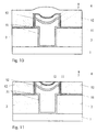
- the first passivation layer 5 has a thickness of approximately 20 nm and serves to prevent corrosion of the copper, which would arise if the copper with the insulating layer 2 in Connection would come. This first passivation layer 5 serves at the same time as a diffusion barrier.
- the first passivation layer 5 (liner) can be tantalum Ta, tantalum nitride or TaN have both materials.
- the first passivation layer 5 2 covers both the first insulating layer 2 and also the area of the substrate 1 in which the first insulating layer 2 was removed.
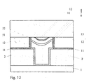
- the metal layer 6 is between 300 nm and 500 nm, preferably approximately 350 nm thick.
- the second passivation layer 7 has approximately the same thickness as the first passivation layer 2, namely approximately 20 nm. Also in the material composition the second passivation layer 7 correspond to the first passivation layer 5.
- the metal layer 6 can be applied by electroplating become. Copper is used as the metal. Copper has the advantage that there is a relatively low ohmic resistance having.
- layer 8 In the layer structure shown in Figure 4 is above second passivation layer 7 a layer 8 with a Layer thickness of approximately 250 nm has been applied. This After structuring, layer 8 serves as a hard mask. As Material is silicon nitride or silicon oxynitride. The hard mask material 8 can be deposited by chemical vapor deposition (CVD).
- an anti-reflective layer 9 applied, among other things also the depth of the dent in the middle area of the Layer 8 reduced.
- the antireflection layer 8 is advantageously used organic material for use.
- a photomask 10 made of photoresist.
- the layer structure shown in FIG. 6 results.
- the etching continues until the second passivation layer 7 is reached.
- the second passivation layer is allowed 7 cannot be etched through.
- the photomask 10 and the anti-reflective layer 9 removed. This results in the one shown in FIG. 7 Layer structure.
- the removal of the photomask 10 and the anti-reflective layer 9 is done by dry stripping without wet cleaning.
- the second passivation layer 7 and the metal layer 6 in the by Removed hard mask predetermined areas can by reactive ion etching or by sputtering.
- the structuring of the copper metal layer 6 by means of reactive Ion etching (RIE) can be performed with caustic gases, such as Hydrochloric acid HCl or chlorine Cl2 supported by Ar or Ar Xenon Xe done.
- caustic gases such as Hydrochloric acid HCl or chlorine Cl2 supported by Ar or Ar Xenon Xe done.
- the first passivation layer 5 is bombarded by ions (Sputtering) sputtered from the first insulating layer 2 and at least partially as a sidewall passivation 52 to the lateral region of the metal layer 6, the second insulating layer 7 and the hard mask 8 sputtered on.
- the chemically active components e.g. Cl2
- the chemically active components e.g. Cl2
- Passivation of the side walls can occur during the etching by adding an additive.
- Inorganic can be used as an additive Material such as nitrogen N2 or oxygen O2 can be used. Comes as an organic material CHF3 or CH4 for use.
- This passivation layer must be used during the sputtering step be removed again.
- FIG Passivation layer 11 a covering with a third can be used according to FIG Passivation layer 11 take place.
- the third passivation layer 11 covers parts of the first insulating layer 2, parts of the first passivation layer 5 and the hard mask 8th.
- the third passivation layer 11 has a layer thickness of about 30 nm and can have silicon nitride. The third Passivation layer 11 is only required if the Passivation layer 52 is not sufficient.
- the second insulating layer 12 is also a dielectric, for example a silicon oxide or a material whose Dielectric constant lower than that of silicon oxide and has a layer thickness of approximately 600 nm.
- CMP chemically mechanically polished
- a third insulating layer 13 which is also a Oxide can be applied.
- the third layer of insulation 13 has a layer thickness of approximately 600 nm.
- the insulating layer 13 can in turn, as shown in Figure 1, structured become. This is a repetition of the above Process steps possible. Overall, an integrated Circuit with multiple metal layers by repetition of the previous process steps are generated.
- the method according to the invention has a dual damascene
- the advantage of this method is that the path etching Contact hole edge does not form a degree (fence). With the dual damascene This process can disadvantageously diminish this degree Lead metal cross section. This can cause reliability problems result, that is, the metal traces may not have the required electrical Properties (low ohmic resistance) correspond.
- Another advantage of the method according to the invention is in that the etching of the copper by reactive ion etching at a high temperature is possible because the hard mask 8 does not evaporate.
- the one for reactive ion etching necessary temperature can be ESC heating or lamp heating (e.g. halogen lamps) of the wafer through the top window of the chamber or possibly also done from below. It is also possible that necessary temperature through targeted heating of the wafer surface, for example by an Ar / Xe sputtering step on the second passivation layer 5 with high RF power and turn off wafer cooling.
- the immediate passivation of the Side walls through the special process control according to the invention the critical phase for the corrosion of copper, namely the wafer transfer or the period from End of etching process until cleaning and subsequent passivation, avoided.
- the method according to the invention can easily be used for use the most diverse types of semiconductor circuits.
Landscapes
- Internal Circuitry In Semiconductor Integrated Circuit Devices (AREA)
Abstract
Description
- Figur 1
- zeigt den Schichtaufbau mit Substrat, Isolierschicht, Antireflexschicht und Photolack und bereits vorhandenem Kontaktierungsloch.
- Figur 2
- zeigt den Schichtaufbau nach dem Entfernen der Photolackschicht und der Antireflexschicht und bereits aufgebrachter erster Passivierungsschicht.
- Figur 3
- zeigt den Schichtaufbau mit Metallfüllung des Kontaktierungslochs und der zweiten Passivierungsschicht.
- Figur 4
- zeigt den Schichtaufbau mit zusätzlich abgeschiedenem Hartmaskenmaterial.
- Figur 5
- zeigt den Schichtaufbau mit aufgebrachter Antireflexschicht und Photolackmaske.
- Figur 6
- zeigt den Schichtaufbau mit bereits strukturierter Hartmaske.
- Figur 7
- zeigt den Schichtaufbau nach dem Entfernen der Photolackmaske und der Antireflexschicht.
- Figur 8
- zeigt den Schichtaufbau nach dem teilweisen Entfernen der zweiten Passivierungsschicht, der Metallschicht und der ersten Passivierungsschicht sowie der Ablagerung der Passivierungsschicht an den Seitenwänden.
- Figur 9
- zeigt den Schichtaufbau mit optionaler dritter Passivierungsschicht.
- Figur 10
- zeigt den Schichtaufbau mit optionaler Passivierungsschicht und einer zweiten Isolierschicht.
- Figur 11
- zeigt den Schichtaufbau nach chemisch mechanischem Polieren.
- Figur 12
- zeigt den Schichtaufbau mit optionaler Passivierungsschicht und einer dritten Isolierschicht.
Claims (18)
- Verfahren zur Herstellung einer Leiterstruktur für einen integrierten Schaltkreis,bei dem auf eine strukturierte erste Isolierschicht (2) eine erste Passivierungsschicht (5) aufgebracht wird,bei dem auf die erste Passivierungsschicht (5) eine Schicht leitenden Materials (6) aufgebracht wird,bei dem auf die Schicht leitenden Materials (6) eine zweite Passivierungsschicht (7) aufgebracht wird,bei dem auf die zweite Passivierungsschicht (7) eine Hartmaske (8) aufgebracht wird,bei dem die Schicht leitenden Materials (6) in den durch die Hartmaske (8) vorgesehenen Bereichen entfernt wird,bei dem die erste Passivierungsschicht (5) in den durch die Hartmaske (8) vorgesehenen Bereichen durch Sputtern entfernt und an der Seitenwand der Schicht leitenden Materials (6) wenigstens zum Teil wieder abgelagert wird.
- Verfahren nach Patentanspruch 1,
bei dem das Entfernen der Schicht leitenden Materials (6) durch reaktives Ionenätzen erfolgt. - Verfahren nach Patentanspruch 1,
bei dem das Entfernen der Schicht leitenden Materials (6) durch Sputtern erfolgt. - Verfahren nach einem der Patentansprüche 1 bis 3,
bei dem die Schicht leitenden Materials (6) Kupfer aufweist. - Verfahren nach einem der Patentansprüche 1 bis 4,
bei dem die Schichtstärke des leitenden Materials (6) zwischen 300 nm und 500 nm beträgt. - Verfahren nach einem der Patentansprüche 1 bis 5,
bei dem die Passivierungsschichten (5, 7) Tantal oder Tantalnitrid oder beides aufweisen. - Verfahren nach einem der Patentansprüche 1 bis 6,
bei dem die erste Isolierschicht (2) ein Siliziumoxid oder ein Material mit einer Dielektrizitätskonstante, die niedriger als die von Siliziumoxid ist, aufweist. - Verfahren nach einem der Patentansprüche 1 bis 7,
bei dem die Hartmaske (8) Siliziumoxid, Siliziumnitrid oder Siliziumoxinitrid aufweist. - Verfahren nach einem der Patentansprüche 1 bis 8,
bei dem die Hartmaske (8) annähernd zwischen 100 nm und 300 nm dick ist. - Verfahren nach einem der Patentansprüche 1 bis 9,
bei dem die erste und die zweite Passivierungsschicht (5,7) jeweils annähernd 20 nm dick sind. - Verfahren nach einem der Patentansprüche 1 bis 10,
bei dem die Oberfläche mit einer dritten Passivierungsschicht (11) versehen wird. - Verfahren nach einem der Patentansprüche 1 bis 11,
bei dem die Oberfläche mit einer zweiten Isolierschicht (12) versehen wird. - Verfahren nach Patentanspruch 12,
bei dem die Oberfläche chemisch mechanisch poliert wird. - Verfahren nach einem der Patentansprüche 1 bis 13,
bei dem beim Sputtern der Wafer gekühlt wird. - Verfahren nach einem der Patentansprüche 1 bis 14,
bei dem beim Sputtern Stickstoff zugeführt wird. - Verfahren nach einem der Patentansprüche 1 bis 15,
bei dem die strukturierte erste Isolierschicht (2) durch reaktive Ionenätzung erzeugt wird. - Verfahren nach einem der Patentansprüche 1 bis 16,
bei dem die Strukturierung der Schicht leitenden Materials (6) durch Aufheizen des Wafers und anschließendem reaktiven Ionenätzen erfolgt. - Verfahren nach einem der Patentansprüche 1 bis 17,
bei dem die Hartmaske (8) durch folgende Schritte erzeugt wird:das Hartmaskenmaterial wird durch chemical vapor deposition abgeschieden,eine Antireflexschicht (9) wird aufgebracht,eine Photolackmaske (10) wird aufgebracht,das Hartmaskenmaterial wird an den durch die Photolackmaske (10) vorgesehenen Bereichen abgeätzt,die Antireflexschicht (9) und die Photolackmaske (10) wird entfernt.
Applications Claiming Priority (2)
| Application Number | Priority Date | Filing Date | Title |
|---|---|---|---|
| DE10011886 | 2000-03-07 | ||
| DE10011886A DE10011886A1 (de) | 2000-03-07 | 2000-03-07 | Verfahren zur Herstellung einer Leiterstruktur für einen integrierten Schaltkreis |
Publications (3)
| Publication Number | Publication Date |
|---|---|
| EP1132957A2 true EP1132957A2 (de) | 2001-09-12 |
| EP1132957A3 EP1132957A3 (de) | 2003-02-05 |
| EP1132957B1 EP1132957B1 (de) | 2007-08-22 |
Family
ID=7634340
Family Applications (1)
| Application Number | Title | Priority Date | Filing Date |
|---|---|---|---|
| EP01103715A Expired - Lifetime EP1132957B1 (de) | 2000-03-07 | 2001-02-15 | Verfahren zur Herstellung einer Leiterstruktur für einen integrierten Schaltkreis |
Country Status (4)
| Country | Link |
|---|---|
| US (1) | US6541372B2 (de) |
| EP (1) | EP1132957B1 (de) |
| DE (2) | DE10011886A1 (de) |
| TW (1) | TW515042B (de) |
Families Citing this family (10)
| Publication number | Priority date | Publication date | Assignee | Title |
|---|---|---|---|---|
| JP3440057B2 (ja) * | 2000-07-05 | 2003-08-25 | 唯知 須賀 | 半導体装置およびその製造方法 |
| US6979526B2 (en) * | 2002-06-03 | 2005-12-27 | Infineon Technologies Ag | Lithography alignment and overlay measurement marks formed by resist mask blocking for MRAMs |
| US6858441B2 (en) * | 2002-09-04 | 2005-02-22 | Infineon Technologies Ag | MRAM MTJ stack to conductive line alignment method |
| US7223612B2 (en) * | 2004-07-26 | 2007-05-29 | Infineon Technologies Ag | Alignment of MTJ stack to conductive lines in the absence of topography |
| US7442624B2 (en) * | 2004-08-02 | 2008-10-28 | Infineon Technologies Ag | Deep alignment marks on edge chips for subsequent alignment of opaque layers |
| US7553718B2 (en) * | 2005-01-28 | 2009-06-30 | Texas Instruments Incorporated | Methods, systems and structures for forming semiconductor structures incorporating high-temperature processing steps |
| US7348272B2 (en) * | 2005-08-03 | 2008-03-25 | United Microelectronics Corp. | Method of fabricating interconnect |
| JP5581005B2 (ja) | 2008-12-26 | 2014-08-27 | 株式会社東芝 | 半導体装置の製造方法 |
| US10134754B2 (en) * | 2017-03-13 | 2018-11-20 | Macronix International Co., Ltd. | Method for forming a 3-D memory device and the 3-D memory device formed thereby |
| US12476116B2 (en) * | 2022-12-15 | 2025-11-18 | Nanya Technology Corporation | Semiconductor structure with anti-back-sputter layer |
Family Cites Families (27)
| Publication number | Priority date | Publication date | Assignee | Title |
|---|---|---|---|---|
| US4026742A (en) * | 1972-11-22 | 1977-05-31 | Katsuhiro Fujino | Plasma etching process for making a microcircuit device |
| US4215156A (en) * | 1977-08-26 | 1980-07-29 | International Business Machines Corporation | Method for fabricating tantalum semiconductor contacts |
| US4184909A (en) * | 1978-08-21 | 1980-01-22 | International Business Machines Corporation | Method of forming thin film interconnection systems |
| US4312113A (en) * | 1978-10-23 | 1982-01-26 | Eaton Corporation | Method of making field-effect transistors with micron and submicron gate lengths |
| US4362597A (en) * | 1981-01-19 | 1982-12-07 | Bell Telephone Laboratories, Incorporated | Method of fabricating high-conductivity silicide-on-polysilicon structures for MOS devices |
| US4742014A (en) * | 1985-05-10 | 1988-05-03 | Texas Instruments Incorporated | Method of making metal contacts and interconnections for VLSI devices with copper as a primary conductor |
| US5229325A (en) * | 1991-01-31 | 1993-07-20 | Samsung Electronics Co., Ltd. | Method for forming metal wirings of semiconductor device |
| JPH0541380A (ja) * | 1991-08-06 | 1993-02-19 | Fujitsu Ltd | 半導体装置の製造方法 |
| US5739579A (en) * | 1992-06-29 | 1998-04-14 | Intel Corporation | Method for forming interconnections for semiconductor fabrication and semiconductor device having such interconnections |
| US5366929A (en) * | 1993-05-28 | 1994-11-22 | Cypress Semiconductor Corp. | Method for making reliable selective via fills |
| KR0144085B1 (ko) * | 1994-12-05 | 1998-08-17 | 김주용 | 반도체 소자의 금속배선 형성방법 |
| JP2679680B2 (ja) * | 1995-04-24 | 1997-11-19 | 日本電気株式会社 | 半導体装置の製造方法 |
| US5825609A (en) * | 1996-04-23 | 1998-10-20 | International Business Machines Corporation | Compound electrode stack capacitor |
| KR100414746B1 (ko) * | 1996-12-31 | 2004-03-31 | 주식회사 하이닉스반도체 | 반도체소자의금속배선형성방법 |
| US6017816A (en) * | 1997-02-25 | 2000-01-25 | Mosel Vitelic Inc. | Method of fabricating A1N anti-reflection coating on metal layer |
| US5998296A (en) * | 1997-04-16 | 1999-12-07 | Texas Instruments Incorporated | Method of forming contacts and vias in semiconductor |
| US5985762A (en) * | 1997-05-19 | 1999-11-16 | International Business Machines Corporation | Method of forming a self-aligned copper diffusion barrier in vias |
| US5846884A (en) * | 1997-06-20 | 1998-12-08 | Siemens Aktiengesellschaft | Methods for metal etching with reduced sidewall build up during integrated circuit manufacturing |
| US6010603A (en) * | 1997-07-09 | 2000-01-04 | Applied Materials, Inc. | Patterned copper etch for micron and submicron features, using enhanced physical bombardment |
| US6027860A (en) * | 1997-08-13 | 2000-02-22 | Micron Technology, Inc. | Method for forming a structure using redeposition of etchable layer |
| US6114242A (en) * | 1997-12-05 | 2000-09-05 | Taiwan Semiconductor Manufacturing Company | MOCVD molybdenum nitride diffusion barrier for Cu metallization |
| US6391771B1 (en) * | 1998-07-23 | 2002-05-21 | Applied Materials, Inc. | Integrated circuit interconnect lines having sidewall layers |
| JP2943805B1 (ja) * | 1998-09-17 | 1999-08-30 | 日本電気株式会社 | 半導体装置及びその製造方法 |
| US6277726B1 (en) * | 1998-12-09 | 2001-08-21 | National Semiconductor Corporation | Method for decreasing contact resistance of an electrode positioned inside a misaligned via for multilevel interconnects |
| JP3353727B2 (ja) * | 1998-12-21 | 2002-12-03 | 日本電気株式会社 | 半導体装置の配線構造の形成方法 |
| US6130162A (en) * | 1999-01-04 | 2000-10-10 | Taiwan Semiconductor Manufacturing Company | Method of preparing passivated copper line and device manufactured thereby |
| US6372645B1 (en) * | 1999-11-15 | 2002-04-16 | Taiwan Semiconductor Manufacturing Company | Methods to reduce metal bridges and line shorts in integrated circuits |
-
2000
- 2000-03-07 DE DE10011886A patent/DE10011886A1/de not_active Withdrawn
-
2001
- 2001-02-15 EP EP01103715A patent/EP1132957B1/de not_active Expired - Lifetime
- 2001-02-15 DE DE50112895T patent/DE50112895D1/de not_active Expired - Lifetime
- 2001-03-06 TW TW090105115A patent/TW515042B/zh not_active IP Right Cessation
- 2001-03-07 US US09/801,213 patent/US6541372B2/en not_active Expired - Lifetime
Also Published As
| Publication number | Publication date |
|---|---|
| DE10011886A1 (de) | 2001-09-20 |
| EP1132957A3 (de) | 2003-02-05 |
| US6541372B2 (en) | 2003-04-01 |
| EP1132957B1 (de) | 2007-08-22 |
| DE50112895D1 (de) | 2007-10-04 |
| TW515042B (en) | 2002-12-21 |
| US20020009876A1 (en) | 2002-01-24 |
Similar Documents
| Publication | Publication Date | Title |
|---|---|---|
| DE69901142T2 (de) | Verfahren zur Herstellung einer Halbleiterschaltung mit Kupfer-Verbindungsleitungen | |
| DE60012807T2 (de) | Plasma-Reinigungsverfahren für Öffnungen in Isolierschicht(en) niedriger Dielektrizitätskonstante über Kupferleitungs-IC-Strukturen | |
| DE69529775T2 (de) | Verfahren zur Herstellung einer Damaszenstruktur mit einer WGe Polierstoppschicht | |
| DE69329663T2 (de) | Verfahren zur Herstellung einer konformen Feuerfestmetallschicht in einer submikronischen Öffnung | |
| DE69213928T2 (de) | Verdrahtung auf Wolfram-Plomben | |
| DE102009023377B4 (de) | Verfahren zur Herstellung eines Mikrostrukturbauelements mit einer Metallisierungsstruktur mit selbstjustiertem Luftspalt | |
| DE69226133T2 (de) | Verbindungsstruktur einer Halbleiteranordnung und ein Herstellungsverfahren dafür | |
| DE60038423T2 (de) | Verfahren zur Herstellung eines Halbleiterbauelements | |
| DE69835032T2 (de) | Verbesserte methode eine oxidschicht zu ätzen | |
| DE60129566T2 (de) | Verfahren zur selektiven ätzung von oxidschichten | |
| DE69025300T2 (de) | Integrierte Schaltung mit einer planarisierten dielektrischen Schicht | |
| DE69023541T2 (de) | Kontaktstruktur für integrierte Halbleiterschaltung. | |
| DE69033615T2 (de) | Ätzen von Kontaktlöchern in einer dielektrischen Doppelschicht mit einer einzigen Ätzkammer | |
| DE102004005697B4 (de) | Herstellungsverfahren für eine widerstandsfähige Via-Struktur und zugehörige Via-Struktur | |
| DE4214091C2 (de) | ||
| DE102008054068A1 (de) | Veringern von Metallhohlräumen in einem metallischen Schichtstapel eines Halbleiterbauelements durch Vorsehen einer dielektrischen Barrierenschicht | |
| DE10244570A1 (de) | Liner-Schicht mit geringer Stufenüberdeckung zur Verbesserung des Kontaktwiderstands bei W-Kontakten | |
| EP1132957B1 (de) | Verfahren zur Herstellung einer Leiterstruktur für einen integrierten Schaltkreis | |
| DE102007009913B4 (de) | Plasmaätzprozess mit hoher Ausbeute für Zwischenschichtdielektrika | |
| DE10341059B4 (de) | Integrierte Schaltungsanordnung mit Kondensator und Herstellungsverfahren | |
| US5776832A (en) | Anti-corrosion etch process for etching metal interconnections extending over and within contact openings | |
| DE102019218942B4 (de) | Herstellung von Verbindungsstrukturen mit Luftspalten und Verbindungen bedeckt mit einem Dielektrikum | |
| DE10085212B4 (de) | Dielektrische Schicht, integrierte Schaltung und Verfahren zu deren Herstellung | |
| DE19719909A1 (de) | Zweifaches Damaszierverfahren | |
| DE10303925B4 (de) | Dielektrische Barrierenschicht für eine Kupfermetallisierungsschicht mit einer über die Dicke hinweg variierenden Siliziumkonzentration und Verfahren zu deren Herstellung |
Legal Events
| Date | Code | Title | Description |
|---|---|---|---|
| PUAI | Public reference made under article 153(3) epc to a published international application that has entered the european phase |
Free format text: ORIGINAL CODE: 0009012 |
|
| AK | Designated contracting states |
Kind code of ref document: A2 Designated state(s): AT BE CH CY DE DK ES FI FR GB GR IE IT LI LU MC NL PT SE TR |
|
| AX | Request for extension of the european patent |
Free format text: AL;LT;LV;MK;RO;SI |
|
| PUAL | Search report despatched |
Free format text: ORIGINAL CODE: 0009013 |
|
| AK | Designated contracting states |
Designated state(s): AT BE CH CY DE DK ES FI FR GB GR IE IT LI LU MC NL PT SE TR |
|
| AX | Request for extension of the european patent |
Extension state: AL LT LV MK RO SI |
|
| RIC1 | Information provided on ipc code assigned before grant |
Ipc: 7H 01L 23/532 B Ipc: 7H 01L 21/3213 B Ipc: 7H 01L 21/768 A |
|
| 17P | Request for examination filed |
Effective date: 20030228 |
|
| 17Q | First examination report despatched |
Effective date: 20030627 |
|
| AKX | Designation fees paid |
Designated state(s): DE FR GB IE IT |
|
| GRAP | Despatch of communication of intention to grant a patent |
Free format text: ORIGINAL CODE: EPIDOSNIGR1 |
|
| GRAS | Grant fee paid |
Free format text: ORIGINAL CODE: EPIDOSNIGR3 |
|
| GRAA | (expected) grant |
Free format text: ORIGINAL CODE: 0009210 |
|
| AK | Designated contracting states |
Kind code of ref document: B1 Designated state(s): DE FR GB IE IT |
|
| REG | Reference to a national code |
Ref country code: GB Ref legal event code: FG4D Free format text: NOT ENGLISH |
|
| REG | Reference to a national code |
Ref country code: IE Ref legal event code: FG4D Free format text: LANGUAGE OF EP DOCUMENT: GERMAN |
|
| REF | Corresponds to: |
Ref document number: 50112895 Country of ref document: DE Date of ref document: 20071004 Kind code of ref document: P |
|
| GBV | Gb: ep patent (uk) treated as always having been void in accordance with gb section 77(7)/1977 [no translation filed] |
Effective date: 20070822 |
|
| REG | Reference to a national code |
Ref country code: IE Ref legal event code: FD4D |
|
| EN | Fr: translation not filed | ||
| PG25 | Lapsed in a contracting state [announced via postgrant information from national office to epo] |
Ref country code: GB Free format text: LAPSE BECAUSE OF FAILURE TO SUBMIT A TRANSLATION OF THE DESCRIPTION OR TO PAY THE FEE WITHIN THE PRESCRIBED TIME-LIMIT Effective date: 20070822 Ref country code: IE Free format text: LAPSE BECAUSE OF FAILURE TO SUBMIT A TRANSLATION OF THE DESCRIPTION OR TO PAY THE FEE WITHIN THE PRESCRIBED TIME-LIMIT Effective date: 20070822 |
|
| PLBE | No opposition filed within time limit |
Free format text: ORIGINAL CODE: 0009261 |
|
| STAA | Information on the status of an ep patent application or granted ep patent |
Free format text: STATUS: NO OPPOSITION FILED WITHIN TIME LIMIT |
|
| 26N | No opposition filed |
Effective date: 20080526 |
|
| PG25 | Lapsed in a contracting state [announced via postgrant information from national office to epo] |
Ref country code: IT Free format text: LAPSE BECAUSE OF NON-PAYMENT OF DUE FEES Effective date: 20080229 |
|
| PG25 | Lapsed in a contracting state [announced via postgrant information from national office to epo] |
Ref country code: FR Free format text: LAPSE BECAUSE OF FAILURE TO SUBMIT A TRANSLATION OF THE DESCRIPTION OR TO PAY THE FEE WITHIN THE PRESCRIBED TIME-LIMIT Effective date: 20080418 |
|
| REG | Reference to a national code |
Ref country code: DE Ref legal event code: R081 Ref document number: 50112895 Country of ref document: DE Owner name: INFINEON TECHNOLOGIES AG, DE Free format text: FORMER OWNER: QIMONDA AG, 81739 MUENCHEN, DE Ref country code: DE Ref legal event code: R081 Ref document number: 50112895 Country of ref document: DE Owner name: POLARIS INNOVATIONS LTD., IE Free format text: FORMER OWNER: QIMONDA AG, 81739 MUENCHEN, DE |
|
| PGFP | Annual fee paid to national office [announced via postgrant information from national office to epo] |
Ref country code: DE Payment date: 20150414 Year of fee payment: 15 |
|
| REG | Reference to a national code |
Ref country code: DE Ref legal event code: R081 Ref document number: 50112895 Country of ref document: DE Owner name: POLARIS INNOVATIONS LTD., IE Free format text: FORMER OWNER: INFINEON TECHNOLOGIES AG, 85579 NEUBIBERG, DE |
|
| REG | Reference to a national code |
Ref country code: DE Ref legal event code: R119 Ref document number: 50112895 Country of ref document: DE |
|
| PG25 | Lapsed in a contracting state [announced via postgrant information from national office to epo] |
Ref country code: DE Free format text: LAPSE BECAUSE OF NON-PAYMENT OF DUE FEES Effective date: 20160901 |