EP1122735B1 - Verschachtelter Datenpfad und Ausgabesteuerungsarchitektur für einen verschachtelten Speicher sowie Impulsgeber zum Ausgeben von gelesenen Daten - Google Patents
Verschachtelter Datenpfad und Ausgabesteuerungsarchitektur für einen verschachtelten Speicher sowie Impulsgeber zum Ausgeben von gelesenen Daten Download PDFInfo
- Publication number
- EP1122735B1 EP1122735B1 EP00830291A EP00830291A EP1122735B1 EP 1122735 B1 EP1122735 B1 EP 1122735B1 EP 00830291 A EP00830291 A EP 00830291A EP 00830291 A EP00830291 A EP 00830291A EP 1122735 B1 EP1122735 B1 EP 1122735B1
- Authority
- EP
- European Patent Office
- Prior art keywords
- data
- register
- load
- read
- output
- Prior art date
- Legal status (The legal status is an assumption and is not a legal conclusion. Google has not performed a legal analysis and makes no representation as to the accuracy of the status listed.)
- Expired - Lifetime
Links
Images


Classifications
-
- G—PHYSICS
- G11—INFORMATION STORAGE
- G11C—STATIC STORES
- G11C7/00—Arrangements for writing information into, or reading information out from, a digital store
- G11C7/10—Input/output [I/O] data interface arrangements, e.g. I/O data control circuits, I/O data buffers
- G11C7/1051—Data output circuits, e.g. read-out amplifiers, data output buffers, data output registers, data output level conversion circuits
- G11C7/1057—Data output buffers, e.g. comprising level conversion circuits, circuits for adapting load
-
- G—PHYSICS
- G11—INFORMATION STORAGE
- G11C—STATIC STORES
- G11C7/00—Arrangements for writing information into, or reading information out from, a digital store
- G11C7/10—Input/output [I/O] data interface arrangements, e.g. I/O data control circuits, I/O data buffers
- G11C7/1015—Read-write modes for single port memories, i.e. having either a random port or a serial port
- G11C7/1018—Serial bit line access mode, e.g. using bit line address shift registers, bit line address counters, bit line burst counters
-
- G—PHYSICS
- G11—INFORMATION STORAGE
- G11C—STATIC STORES
- G11C7/00—Arrangements for writing information into, or reading information out from, a digital store
- G11C7/10—Input/output [I/O] data interface arrangements, e.g. I/O data control circuits, I/O data buffers
- G11C7/1015—Read-write modes for single port memories, i.e. having either a random port or a serial port
- G11C7/1039—Read-write modes for single port memories, i.e. having either a random port or a serial port using pipelining techniques, i.e. using latches between functional memory parts, e.g. row/column decoders, I/O buffers, sense amplifiers
-
- G—PHYSICS
- G11—INFORMATION STORAGE
- G11C—STATIC STORES
- G11C7/00—Arrangements for writing information into, or reading information out from, a digital store
- G11C7/10—Input/output [I/O] data interface arrangements, e.g. I/O data control circuits, I/O data buffers
- G11C7/1015—Read-write modes for single port memories, i.e. having either a random port or a serial port
- G11C7/1042—Read-write modes for single port memories, i.e. having either a random port or a serial port using interleaving techniques, i.e. read-write of one part of the memory while preparing another part
-
- G—PHYSICS
- G11—INFORMATION STORAGE
- G11C—STATIC STORES
- G11C7/00—Arrangements for writing information into, or reading information out from, a digital store
- G11C7/10—Input/output [I/O] data interface arrangements, e.g. I/O data control circuits, I/O data buffers
- G11C7/1015—Read-write modes for single port memories, i.e. having either a random port or a serial port
- G11C7/1045—Read-write mode select circuits
-
- G—PHYSICS
- G11—INFORMATION STORAGE
- G11C—STATIC STORES
- G11C7/00—Arrangements for writing information into, or reading information out from, a digital store
- G11C7/10—Input/output [I/O] data interface arrangements, e.g. I/O data control circuits, I/O data buffers
- G11C7/1051—Data output circuits, e.g. read-out amplifiers, data output buffers, data output registers, data output level conversion circuits
- G11C7/106—Data output latches
-
- G—PHYSICS
- G11—INFORMATION STORAGE
- G11C—STATIC STORES
- G11C7/00—Arrangements for writing information into, or reading information out from, a digital store
- G11C7/10—Input/output [I/O] data interface arrangements, e.g. I/O data control circuits, I/O data buffers
- G11C7/1051—Data output circuits, e.g. read-out amplifiers, data output buffers, data output registers, data output level conversion circuits
- G11C7/1069—I/O lines read out arrangements
-
- G—PHYSICS
- G11—INFORMATION STORAGE
- G11C—STATIC STORES
- G11C7/00—Arrangements for writing information into, or reading information out from, a digital store
- G11C7/10—Input/output [I/O] data interface arrangements, e.g. I/O data control circuits, I/O data buffers
- G11C7/1072—Input/output [I/O] data interface arrangements, e.g. I/O data control circuits, I/O data buffers for memories with random access ports synchronised on clock signal pulse trains, e.g. synchronous memories, self timed memories
-
- G—PHYSICS
- G11—INFORMATION STORAGE
- G11C—STATIC STORES
- G11C7/00—Arrangements for writing information into, or reading information out from, a digital store
- G11C7/22—Read-write [R-W] timing or clocking circuits; Read-write [R-W] control signal generators or management
-
- G—PHYSICS
- G11—INFORMATION STORAGE
- G11C—STATIC STORES
- G11C8/00—Arrangements for selecting an address in a digital store
- G11C8/04—Arrangements for selecting an address in a digital store using a sequential addressing device, e.g. shift register, counter
-
- G—PHYSICS
- G11—INFORMATION STORAGE
- G11C—STATIC STORES
- G11C8/00—Arrangements for selecting an address in a digital store
- G11C8/18—Address timing or clocking circuits; Address control signal generation or management, e.g. for row address strobe [RAS] or column address strobe [CAS] signals
Definitions
- the present invention relates in general to memory devices and in particular to interleaved memories, readable in synchronous mode by successive locations with a sequential type of access, commonly referred to as burst mode, and to standard memories read in a random access asynchronous mode with fast access times.
- a read cycle is defined from a request of data effected by way of the input of a new address, to the final output of the bits stored in the addressed location (byte, word, etc.).
- the reading process evolves through several steps (from the acquisition of the new address, to its decoding, to the generation of synchronizing pulses of the sensing circuits, to the output of the read datum, and the like).
- the ATD (Address Transition Detection) signal recognizes a change of the address input by the external circuitry and therefore the new request of access and initiates a new read cycle.
- an equalization of the sensing circuitry takes place, at the end of which as timed by the signal EQZ , the effective reading of the memory cells takes place.
- the recording of the read datum into the latches in cascade to the sense amplifiers takes place, from where the read word may be transferred to the output buffers.
- the reading process exploits the fact that the reading takes place by successive locations, that is the subsequent memory location to be read and therefore its address is predictable from the address of the location being currently read.
- a subgroup of these sequential (burst) synchronous read mode memories is represented by the so-called interleaved memories.
- a burst access interleaved memory is described in US Patent No. 5,559,990 .
- the cell array is divided in two semi-arrays or banks, each having its own read circuitry.
- the read streams of the two banks are thereafter superimposed though, according to one of the most commonly followed approaches, outphased from each other. While on one of the two banks or semi-array the steps of evaluation and transfer of the datum to the output are being performed, on the other bank or semi-array (being known the (next) location to be addressed) a new read cycle may be started without waiting for the conclusion of the current read cycle that involves the first semi-array.
- the array is divided in two independent banks or semi-arrays, EVEN and ODD, respectively, each having its own independent read path.
- EVEN e.g.
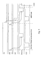
- ODD e.g., a basic scheme of which is depicted in Fig. 1
- the array is divided in two independent banks or semi-arrays, EVEN and ODD, respectively, each having its own independent read path.
- the readings are simultaneous on the two banks, the data read are stored in respective output registers and made available to the outside world in synchronism with an external clock signal.
- the readings on the two semi-arrays have an alternate and interleaved evolution on a time base.
- the first approach though offering a simpler hardware implementation, limits the minimization of the start times of synchronous read cycles. For a better comprehension, it is necessary to consider the basic steps that are performed when passing from an asynchronous read mode to a synchronous read mode. With reference to the scheme of Fig. 2 , and supposing to be starting the reading from an address X, the latter will be loaded on the EVEN bank counter and on the ODD bank counter, less the least significant bit (A0) of the address. The two counters will point the same location X of the respective bank or semi-array.
- known synchronous memory devices do not make any initial increment and wait for the successive cycle for incrementing both counters and therefore read the location X+1 of the banks EVEN and ODD. This makes the times of the first read cycle and of the second sequential read cycle at best equal to the asynchronous read mode time of the memory.
- the efficient management of the read processes has a direct influence of the performance of the memory device.
- a memory device If a memory device is designed to be read in asynchronous mode, it will be generally provided with a rather simple control circuitry of the read data streams, privileging the use of adaptive structures, such as dummy wordlines and dummy sense amplifiers, while leaving the reading circuitry free to evolve as fast as possible, in order to achieve the shortest asynchronous access delays.
- adaptive structures such as dummy wordlines and dummy sense amplifiers
- the access mode in a reading phase of operation is set in base to a specific protocol of use of two of the canonical external protocol signals and precisely in function of the address input latches enabling signal ALE and of the read stimulation signal RD.
- the counters of the two semi-arrays or banks or the counter of the first bank and a more simpler register with functions of address counter of the second bank may also be incremented distinctly from one another such to outphase the readings on the two banks already from the first (asynchronous) read cycle.
- the memory device of the invention is perfectly able to switch to a synchronous mode reading phase at any time, practically halving the access time to such a mode.
- the two distinct reading processes, respectively according to an asynchronous random access mode and according to a synchronous burst access mode remain congruent with each other, having an alternate and interleaved evolution in time, as described in the prior European Patent Application No. 00830068.3, filed on January 31, 2000 .
- the reading of a standard memory is an asynchronous process that, starting from an initial stimulation generated by the switching of at least an external address line, evolves as far as to produce the new datum of the output.
- the US patent No. 5,831,929 discloses a memory device that includes input and output data sequencers that transfer data between a memory array and a data bus where transfers between the data sequencers and the data bus are controlled by a first clock signal and transfers between a memory array and the data sequencers are controlled by a second clock signal.
- GB-A-2 336 924 discloses a semiconductor memory device with common pin for addresses and data.
- the architecture of the invention is based on using three distinct registers, the first two of which are respectively dedicated to store the data read by respective arrays of sense amplifiers of two banks in which is typically divided the cell array of an interleaved memory.
- the third register receives as an input, under control of the timing circuitry of the memory, the data previously stored in one of the other of the first two registers and through an array of pass-gates driven in common by a control signal generated by the timing circuitry, the data so loaded in the third register are eventually transferred to the inputs of the output buffers, which are in turn controlled by external signals of the read protocol of the memory.
- the structure employs three distinct register for storing the data allows to manage in a outstandingly simple manner the operation of the memory device under all conditions contemplated by the protocol.
- the use of three distinct registers permits to perform on the two banks readings substantially uncorrelated among each other.
- the readings may in fact be outphased or simultaneous depending on the starting stimulation and at the end of the read process, the sense amplifiers of each bank update a respective register coupled in cascade on the sense amplifier array of each bank.
- control and timing circuit of the memory includes a special pulse generating circuit for generating signals of interleaved loading of data from the pair of registers in cascade of the two respective banks of sense amplifiers into an output data register and a control circuit of the output buffers that uses a peculiar locking mechanism that allows to advantageously extend the duration of the load pulses of data in the output register and of downloading of the data toward the output buffers.
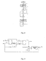
- FIG. 2 A functional diagram of the structure of the invention is depicted in Fig. 2 , wherein the path of data toward the output of the memory is placed in evidence.
- the signals SAEN and SAlatch are generated according to the common sequential logic structures of an interlaced memory but the structures are duplicated for the two banks in the architecture of this invention.
- the protocol may contemplate even the possibility of interrupting a synchronous reading phase with a stand-by period (of a minimum duration equal to the duration of the single synchronous read cycle) after which the sequential reading restarts from the point in which it was interrupted by outputting either the last read datum or the successive datum, depending on the state of the protocol signal RD at the instant of entering the stand-by. Two situations are possible:
- the state machine of the control circuit TIMING of the memory controls the updating of the register DATA OUT REGISTER before the output buffer BUFFOUT even during the stand-by of the memory.
- the TIMING block produces a LOAD pulse that loads the successive datum on the register DATA OUT REGISTER.
- the TIMING block upon resuming operation after a stand-by (Resume), produces a pulse DLATCHN that enables the visibility from outside (on BUFFOUT ) of the datum present on the output data register.
- the protocol may require that the minimum duration of any Resume cycle be equal to that of a synchronous read cycle (for example around 25ns). This time interval would be insufficient to carry out a new complete reading.
- a memory device embodying the data path and output management architecture of the invention has a remarkable flexibility. It can manage a RECOVERY&RESUME cycle as any synchronous cycle. This enhances the robustness because normal asynchronous reading structures are preserved and simplifies to a great measure the internal state machine that controls the memory.
- a fundamental characteristic of the invention is a discontinuity of the coupling between the sense amplifiers and the internal output data bus.
- the architecture contemplates a special control structure producing, only at appropriate instants, an enabling signal for loading a read datum on the internal output data bus, and disconnecting again the sense amplifiers from the internal output data bus, while waiting for a new cycle.
- Such an enabling signal must fulfil fundamental requirements such that the sequential reading process takes place in a correct manner. In particular it must coherently manage both the dependence from the communication protocol between the memory and the external world (thus the synchronization of the output of data) and the information coming from the sense amplifiers on the effective availability of a read datum.
- All interlaced memory systems independently from the protocol, contemplate a first random access, in which a certain address is provided from the outside together with a control bit, i.e. the command ALE (Address Latch Enable), such that the memory acquires and stores it in its input address latches.
- ALE Address Latch Enable
- a first reading cycle commonly defined " MISS CYCLE" begins.
- Such a first read cycle will require a full access interval because it is an asynchronous cycle. Therefore, during this first read cycle, the LOAD signal must be generated by considering the time that is needed for the read datum to be ready at the output of the sense amplifiers before allowing its transfer to the output buffers.
- the other external control signal RD of the communication protocol effectively provides for the synchronization with the external system by virtue of intrinsic function of such a signal of requesting data.
- the LOAD pulse must depend from such a synchronization.
- Fig. 3 illustrates what has been explained above.
- Fig. 4 depicts a global diagram of the structure that comprises:
- the system checks that the reading has evolved to the latching phase, in order to avoid connecting the sense amplifiers to the data bus while they are still in an equalization phase (in which case it could be present an incorrect datum at their outputs or, which is even worse, during the critical reading cause the inputting of switching noise of the output buffers.
- control circuit TIMING depending on the protocol of the system, will have produced an increment pulse INC for the counters of the internal addresses, in order to generate the successive address at which the next reading is to be carried out.
- the presence of such an increment pulse INC confirms that a HIT cycle is going to take place.
- Fig. 4 exploits these information for deciding the best instant for the production of the LOAD signal, using the signals SAlatch and INC.
- the SAlatch signal in generally of a monostable kind, that is it enters in its active phase (in the example it is active-low) to indicate the end of the reading by the sense amplifiers and, after a certain time, or in case of aborted reading, returns to its rest level.
- the first SAlatch is not related to the true MISS cycle, therefore the LOAD pulse must not be generated immediately after the INC pulse, but it is necessary to wait for a new SAlatch. It is evident that the possibility of operating in purely asynchronous mode, synchronous-miss and synchronous-hit, besides the normal management of aborted reading cycles poses a great problem of recognizing the effective reading cycle in progress to manage it in the most appropriate manner.
- the signals INC and SAlatch are used for sending the first LOAD pulse through a sequential structure and the equalization signal EQZ is used to reset the detection flag of SAlatch (in fact, during each reading, the equalization phase precedes the latch phase).
- the first LOAD ( MISS cycle) is generated starting from the rising edge of the signal OK_LOAD, obtained as the logic AND of the two flags coming from two SR flip-flop, namely: the detection flag of INC and the detection flag of SAlatch.
- the flip-flop related to the SAlatch signal is reset at each start of a read cycle by the signal EQZ (which precedes SAlatch just at the beginning of the readings), as far as an INC pulse is detected: from this instant onward it is necessary to leave free the latch to capture the forthcoming SAlatch .
- the flip-flop related to the INC signal must reset (and remain reset) at each detection and for the whole duration of the ALE signal (Address Latch Enable), because only at the end of the latter the sequential cycles (burst) start, and must set at the end of the first INC pulse.
- a last control on the pulser (which generally once stimulated should produce pulses of the same duration) allows a modulation of the duration of this first LOAD pulse making it at least equal to that of the SAlatch pulse.
- a "stretching" of the LOAD signal as far as the SAlatch switches can be advantageously carried out in consideration that the SAlatch signal is built ad hoc for such an aim.
- FIG. 6 The flow-chart of the generation of the LOAD signal of the first MISS cycle is depicted in Fig. 6 .
- the functional diagram of the relative circuital structure is depicted in Fig. 7 .
- the LOAD pulser is driven by the signal RD itself.
- a multiplexer constituted by a "transfer-gate” is used to decouple the pulse generator from OK_LOAD_MISS and couple it directly to the signal RD, so that at each rising edge of the latter the required LOAD pulse is generated.
- the management of the multiplexer may include a master-slave system resetting at the beginning of each MISS cycle with the signal ALE and waiting for the conclusion of the MISS cycle itself. Because, as already said, the first LOAD pulse may have a variable duration (because it depends on the duration of SAlatch ), it is necessary to wait for the end of said LOAD pulse to change the signal input to the MUX.
- the circuit is substantially a monostable circuit capable of deriving the rising edges of the input signal.
- the pulse LOAD that is produced must have an appropriate duration coherent with the time needed to transfer the information from the sense amplifiers to the buffers. That is it is important to make its duration independent from that of RD, but constant in order to make it manageable always in the same manner by the internal logic.
- the LOAD and DLATCHN signals directly affect the reading time of the memory because they determine the update of the output.
- a processing in function of the priority and above all of the outphasing among the signals coming from the sense amplifiers and the external control signals is performed.
- Such a processing is carried out by the block BUFFOUT_CTRL of the control circuit TIMING of the memory, whose function is to produce secondary signals, namely: LOAD_EV and LOAD_OD for a correct transfer of the datum from the output latch of the respective array of sense amplifiers to the data output register and for the generation of the DLATCH signal for transferring the datum from the output register to the output buffers.
- the signal DLATCH is generated by LOAD_EV_ASYNC and LOAD_OD_ASYNC, which are always exactly dependent in an exclusive manner from their respective signals SAlatch_EV and SAlatch_OD that are produced each time a new datum is ready to be output by the sense amplifiers.
- the asynchronous control block In synchronous mode, the asynchronous control block is disabled and the relative LOAD signals ( EV or OD ) are produced by distinct functional blocks as described below.
- this block detects the presence of two simultaneous events (request of output data and updating in progress of the output latch of the sense amplifiers in progress) and in particular the delay condition of the closing of the second event in respect to the first one.
- the particular locking mechanism allows to advantageously extend the associated pulses LOAD and DLATCHN by conditioning them to the end of a complete and correct updating period of the output latches of the sense amplifiers.
- Pre-load LOAD_EV and LOAD_OD this block, the functional circuit diagram of which is depicted in Figs. 12 and 14 , enables the transfer of the datum present in the output latches of the sense amplifiers to the data output register if the current read cycle has terminated before a request of the datum (rising edge of RD ). It must be observed that the signal DLATCHN that remains tied to the effective request by the protocol, is not generated.
- This block detects the external request of the datum being sensible to the primary LOAD signal (produced by the LOAD_PULSER in coincidence with the leading edge of RD ) and starts the generation of an effective specific command LOAD_EV_SYNC or LOAD_OD_SYNC, depending on the priority.
- the width of such a pulse is modulated by the SAlatch signal.
- the starting of the pulses LOAD_EV_SYNC or LOAD_OD_SYNC is established by the primary LOAD signal while their duration depends on the duration of the respective SAlatch signal.
- This block is to anticipate, whenever possible, the transfer of the datum from the output latches of the sense amplifiers to the output data register.
- the updating of the output register is advantageously anticipated even if the effective request of a new datum established by a new rising edge of the external command RD has not yet been detected.
Claims (4)
- Architektur zur Verwaltung eines verschachtelten Datenpfads und von Datenausgabe für einen verschachtelten Speicher, aufgeteilt in zumindest eine erste Bank und eine zweite Bank (EVEN BANK, ODD BANK), die jeweils mit einem Array von Leseverstärkern (EVEN SENSE, ODD SENSE) und einem Register für gelesene Daten (DATA OD REGISTER, DATA EV REGISTER) ausgestattet sind, und umfassend einen Array von Ausgabepuffern (BUFFOUT), und eine Steuerungs- und Zeitgeberschaltungsanordnung (TIMING), die als Eingangssignale externe Protokollsignale (ALE, RD, CE) empfängt und Freigabe- und/oder Pfadauswahlsignale (SAEN_EVEN, SAEN_ODD, SAlatch_EVEN, SAlatch_ODD) erzeugt, und weiterhin umfassend
zumindest ein drittes Register (DATA OUT REGISTER), dessen Eingängen die Ausgangsdaten der Register für aus den beiden Banken gelesene Daten (DATA EV REGISTER, DATA OD REGISTER) zugeführt werden in Abhängigkeit von sekundären Ladeimpulsen (LOAD_EV, LOAD_OD), die von der Steuerungs- und Zeitgeberschaltungsanordnung (TIMING) erzeugt werden;
dadurch gekennzeichnet, dass sie weiterhin umfasst
einen Array von Durchgangsgattem, die gemeinsam durch ein von der Steuerungs-und Zeitgeberschaltungsanordnung (TIMING) erzeugtes Steuerungssignal (DLATCHN) angesteuert werden, das die Übermittlung im dritten Register (DATA OUT REGISTER) gespeicherter Daten an jeweilige Eingänge des Arrays von Ausgabepuffern (BUFFOUT) freigibt;
wobei der Array von Ausgabepuffern (BUFFOUT) durch externe Protokollsignale (CE, OE) angesteuert wird,
wobei die Steuerungs- und Zeitgeberschaltungsanordnung (TIMING) umfasst
eine Steuerungseinrichtung (BUFFOUT CTRL) zur Erzeugung der sekundären Ladeimpulse (LOAD_EV, LOAD_OD) zwecks Freigabe der Übermittlung eines Datenelements aus den Registern für gelesene Daten (DATA OD REGISTER, DATA EV REGISTER) ans dritte Register (DATA_OUT REGISTER) der Banken des Speichers in Abhängigkeit von einem primären Ladeimpuls (LOAD), einem jeweiligen sekundären Signal zur Freigabe der Übermittlung gelesener Daten ans jeweilige Register der Banken (SAlatch_EV, SAlatch_OD) und einem Prioritäts-Flag (PRIORITY), das abwechselnd die eine oder die andere der Banken des Speichers kennzeichnet; und
eine Einrichtung zur Erzeugung eines Steuerungssignals (DLATCHN), das die Pfade von Daten zu den Eingängen der Ausgabepuffer (BUFFOUT) synchron mit den sekundären Ladeimpulsen (LOAD_EV, LOAD_OD) freigibt, die ihrerseits synchronisiert sind mit externen Protokolllesesignalen (CE, ALE, RD), abhängig vom aktuellen Zugriffsmodus. - Architektur nach Anspruch 1, in der die Steuerungs- und Zeitgeberschaltungsanordnung (TIMING) umfasst
einen monostabilen Schaltkreis zur Erzeugung eines primären Impulses (LOAD) zum Laden von Daten ins dritte Register (DATA OUT REGISTER), angesteuert durch einen Einfach-Multiplexer (MUX), von dem ein erster Eingang gekoppelt ist an ein externes Zeitgebersignal (RD) des Leseprotokolls und von dem ein zweiter Eingang gekoppelt ist an den Ausgang eines Schaltkreises (MISS Block) zur Steuerung der Erzeugung des primären Ladeimpulses (LOAD) während asynchroner Lesezyklen mit wahlfreiem Zugriff, der als Eingangssignale ein externes Adressspeicherfreigabesignal (ALE), ein Bestätigungssignal für den Angleich der Leseverstärker (EQZ), einen Inkrementimpuls (INC) interner Adresszähler und ein Freigabesignal (SAlatch_ODD, SAlatch_EVEN) für die Übermittlung der in einem jeweiligen Register für gelesene Daten (DATA OD REGISTER, DATA EV REGISTER) gelesenen Daten empfängt;
einen zweiten Schaltkreis (HIT-Zyklen-Block) zur Steuerung sequenzieller Zugriffszyklen, der als Eingangssignale das externe Signal zur Freigabe der Adressspeicher (ALE) und den primären Ladeimpuls (LOAD) empfängt, und dessen Ausgang gekoppelt ist an den Auswahleingang (Sel) des Multiplexers (MUX) zum Auswählen des an die externen Zeitgebersignale (RD) gekoppelten Eingangs während des Betriebs mit Burst-Zugriff mit Lesephasen im Synchronmodus. - Architektur nach Anspruch 2, gekennzeichnet durch das weitere Umfassen einer Einrichtung zur Modulation der Dauer des primären Ladeimpulses (LOAD) während einer asynchronen Lesephase bei wahlfreiem Zugriffsmodus zwecks Entsprechung der Dauer eines primären Impulses (SAlatch) zur Freigabe der Übermittlung in einem jeweiligen Register für gelesene Daten (DATA OD_REGISTER, DATA EV_REGISTER) gelesener Daten, umfassend ein UND-Gatter mit zwei Eingängen, von denen einem ersten invertierenden Eingang der primäre Freigabeimpuls (SAlatch) zugeführt wird und von denen ein zweiter Eingang an den Ausgang des zweiten Schaltkreises (HIT-Zyklen-Block) gekoppelt ist.
- Architektur nach Anspruch 2, gekennzeichnet durch das Umfassen einer Steuerungseinrichtung, die ein funktionell zwischen den Ausgang des Multiplexers (MUX) und den Eingang des monostabilen Schaltkreises, der den primären Ladeimpuls (LOAD) erzeugt, geschaltetes Durchgangsgatter mit einem an den Ausgang des monostabilen Schaltkreises angeschlossenen Steuereingang umfasst.
Priority Applications (2)
| Application Number | Priority Date | Filing Date | Title |
|---|---|---|---|
| EP00830291A EP1122735B1 (de) | 2000-01-31 | 2000-04-17 | Verschachtelter Datenpfad und Ausgabesteuerungsarchitektur für einen verschachtelten Speicher sowie Impulsgeber zum Ausgeben von gelesenen Daten |
| US09/774,542 US6470431B2 (en) | 2000-01-31 | 2001-01-31 | Interleaved data path and output management architecture for an interleaved memory and load pulser circuit for outputting the read data |
Applications Claiming Priority (3)
| Application Number | Priority Date | Filing Date | Title |
|---|---|---|---|
| EP00830068 | 2000-01-31 | ||
| EP00830068A EP1122734B1 (de) | 2000-01-31 | 2000-01-31 | Verschachtelter Burst-Speicher mit Burst-Zugriff bei synchronen Lesezyklen, wobei die beiden untergeordneten Speicherfelder unabhängig lesbar sind mit wahlfreiem Zugriff während asynchroner Lesezyklen |
| EP00830291A EP1122735B1 (de) | 2000-01-31 | 2000-04-17 | Verschachtelter Datenpfad und Ausgabesteuerungsarchitektur für einen verschachtelten Speicher sowie Impulsgeber zum Ausgeben von gelesenen Daten |
Publications (2)
| Publication Number | Publication Date |
|---|---|
| EP1122735A1 EP1122735A1 (de) | 2001-08-08 |
| EP1122735B1 true EP1122735B1 (de) | 2010-09-01 |
Family
ID=26074116
Family Applications (1)
| Application Number | Title | Priority Date | Filing Date |
|---|---|---|---|
| EP00830291A Expired - Lifetime EP1122735B1 (de) | 2000-01-31 | 2000-04-17 | Verschachtelter Datenpfad und Ausgabesteuerungsarchitektur für einen verschachtelten Speicher sowie Impulsgeber zum Ausgeben von gelesenen Daten |
Country Status (2)
| Country | Link |
|---|---|
| US (1) | US6470431B2 (de) |
| EP (1) | EP1122735B1 (de) |
Families Citing this family (18)
| Publication number | Priority date | Publication date | Assignee | Title |
|---|---|---|---|---|
| EP1122734B1 (de) * | 2000-01-31 | 2005-03-30 | STMicroelectronics S.r.l. | Verschachtelter Burst-Speicher mit Burst-Zugriff bei synchronen Lesezyklen, wobei die beiden untergeordneten Speicherfelder unabhängig lesbar sind mit wahlfreiem Zugriff während asynchroner Lesezyklen |
| EP1122736B1 (de) * | 2000-01-31 | 2009-10-28 | STMicroelectronics S.r.l. | Erzeugung eines Addressenübergangssignals (ATD) für eine synchrone Speicheranordnung |
| EP1199723B1 (de) * | 2000-10-18 | 2008-12-31 | STMicroelectronics S.r.l. | Verschachtelte Speichereinrichtung mit willkürlichem und sequentiellem Zugriff |
| DE10201179B4 (de) * | 2002-01-15 | 2004-02-19 | Infineon Technologies Ag | Digitale Speicherschaltung mit mehreren Speicherbänken |
| US7355470B2 (en) | 2006-04-24 | 2008-04-08 | Parkervision, Inc. | Systems and methods of RF power transmission, modulation, and amplification, including embodiments for amplifier class transitioning |
| US7327803B2 (en) | 2004-10-22 | 2008-02-05 | Parkervision, Inc. | Systems and methods for vector power amplification |
| US8334722B2 (en) | 2007-06-28 | 2012-12-18 | Parkervision, Inc. | Systems and methods of RF power transmission, modulation and amplification |
| US7911272B2 (en) | 2007-06-19 | 2011-03-22 | Parkervision, Inc. | Systems and methods of RF power transmission, modulation, and amplification, including blended control embodiments |
| KR100719378B1 (ko) * | 2006-02-16 | 2007-05-17 | 삼성전자주식회사 | 빠른 랜덤 액세스 기능을 갖는 플래시 메모리 장치 및그것을 포함한 컴퓨팅 시스템 |
| US7937106B2 (en) | 2006-04-24 | 2011-05-03 | ParkerVision, Inc, | Systems and methods of RF power transmission, modulation, and amplification, including architectural embodiments of same |
| US8031804B2 (en) | 2006-04-24 | 2011-10-04 | Parkervision, Inc. | Systems and methods of RF tower transmission, modulation, and amplification, including embodiments for compensating for waveform distortion |
| US8315336B2 (en) | 2007-05-18 | 2012-11-20 | Parkervision, Inc. | Systems and methods of RF power transmission, modulation, and amplification, including a switching stage embodiment |
| US7899005B2 (en) * | 2006-09-12 | 2011-03-01 | Cisco Technology, Inc. | Method and apparatus for passing routing information among mobile routers |
| WO2008156800A1 (en) | 2007-06-19 | 2008-12-24 | Parkervision, Inc. | Combiner-less multiple input single output (miso) amplification with blended control |
| WO2009145887A1 (en) | 2008-05-27 | 2009-12-03 | Parkervision, Inc. | Systems and methods of rf power transmission, modulation, and amplification |
| EP2695294A1 (de) | 2011-04-08 | 2014-02-12 | Parkervision, Inc. | System und verfahren zur hf-leistungsübertragung, -modulation und -verstärkung |
| WO2012167111A2 (en) | 2011-06-02 | 2012-12-06 | Parkervision, Inc. | Antenna control |
| EP3047348A4 (de) | 2013-09-17 | 2016-09-07 | Parkervision Inc | Verfahren, vorrichtung und system für die darstellung einer datenträgerzeitfunktion |
Citations (1)
| Publication number | Priority date | Publication date | Assignee | Title |
|---|---|---|---|---|
| GB2336924A (en) * | 1998-04-03 | 1999-11-03 | Hyundai Electronics Ind | Semiconductor device with common pin for address and data |
Family Cites Families (10)
| Publication number | Priority date | Publication date | Assignee | Title |
|---|---|---|---|---|
| US4800530A (en) * | 1986-08-19 | 1989-01-24 | Kabushiki Kasiha Toshiba | Semiconductor memory system with dynamic random access memory cells |
| US5559990A (en) | 1992-02-14 | 1996-09-24 | Advanced Micro Devices, Inc. | Memories with burst mode access |
| EP0561370B1 (de) | 1992-03-19 | 1999-06-02 | Kabushiki Kaisha Toshiba | Taktsynchronisierter Halbleiterspeicheranordnung und Zugriffsverfahren |
| US5696917A (en) | 1994-06-03 | 1997-12-09 | Intel Corporation | Method and apparatus for performing burst read operations in an asynchronous nonvolatile memory |
| US5596539A (en) | 1995-12-28 | 1997-01-21 | Lsi Logic Corporation | Method and apparatus for a low power self-timed memory control system |
| US5966724A (en) | 1996-01-11 | 1999-10-12 | Micron Technology, Inc. | Synchronous memory device with dual page and burst mode operations |
| US5831929A (en) * | 1997-04-04 | 1998-11-03 | Micron Technology, Inc. | Memory device with staggered data paths |
| JP4060442B2 (ja) | 1998-05-28 | 2008-03-12 | 富士通株式会社 | メモリデバイス |
| JP2000067577A (ja) * | 1998-06-10 | 2000-03-03 | Mitsubishi Electric Corp | 同期型半導体記憶装置 |
| US6111807A (en) * | 1998-07-17 | 2000-08-29 | Mitsubishi Denki Kabushiki Kaisha | Synchronous semiconductor memory device allowing easy and fast text |
-
2000
- 2000-04-17 EP EP00830291A patent/EP1122735B1/de not_active Expired - Lifetime
-
2001
- 2001-01-31 US US09/774,542 patent/US6470431B2/en not_active Expired - Lifetime
Patent Citations (1)
| Publication number | Priority date | Publication date | Assignee | Title |
|---|---|---|---|---|
| GB2336924A (en) * | 1998-04-03 | 1999-11-03 | Hyundai Electronics Ind | Semiconductor device with common pin for address and data |
Also Published As
| Publication number | Publication date |
|---|---|
| US6470431B2 (en) | 2002-10-22 |
| US20010034819A1 (en) | 2001-10-25 |
| EP1122735A1 (de) | 2001-08-08 |
Similar Documents
| Publication | Publication Date | Title |
|---|---|---|
| EP1122735B1 (de) | Verschachtelter Datenpfad und Ausgabesteuerungsarchitektur für einen verschachtelten Speicher sowie Impulsgeber zum Ausgeben von gelesenen Daten | |
| EP1122734B1 (de) | Verschachtelter Burst-Speicher mit Burst-Zugriff bei synchronen Lesezyklen, wobei die beiden untergeordneten Speicherfelder unabhängig lesbar sind mit wahlfreiem Zugriff während asynchroner Lesezyklen | |
| EP1199723B1 (de) | Verschachtelte Speichereinrichtung mit willkürlichem und sequentiellem Zugriff | |
| JP3856696B2 (ja) | 2倍データ速度同期式動的ランダムアクセスメモリのための構成可能同期装置 | |
| US10456819B2 (en) | Memory interface configurable for asynchronous and synchronous operation and for accessing storage from any clock domain | |
| EP1238339B1 (de) | Schnittstelle für eine speichereinheit | |
| CN116521604B (zh) | 一种同步数据的方法及相关装置 | |
| JP2001189076A (ja) | 同期式メモリ装置のデータ出力装置 | |
| CN100442394C (zh) | 半导体存储装置及其控制方法 | |
| US6487140B2 (en) | Circuit for managing the transfer of data streams from a plurality of sources within a system | |
| EP1211603B1 (de) | Multiprozessorschnittstelle | |
| US6625706B2 (en) | ATD generation in a synchronous memory | |
| US6356505B2 (en) | Internal regeneration of the address latch enable (ALE) signal of a protocol of management of a burst interleaved memory and related circuit | |
| EP1122739A2 (de) | Beschleunigte Ubertragungserzeugung | |
| EP1324346A1 (de) | Speicheranordnung | |
| JP3459542B2 (ja) | シリアルデータ転送装置 | |
| JP3184144B2 (ja) | メモリシステム | |
| JPH0614435B2 (ja) | 半導体メモリ | |
| JPH05174570A (ja) | 半導体集積回路 | |
| JPH04156629A (ja) | メモリクロックの制御方式 | |
| JPH06289950A (ja) | スキュー補正データ転送回路 | |
| JPH0696579A (ja) | クロック同期型半導体記憶装置およびそのアクセス方法 |
Legal Events
| Date | Code | Title | Description |
|---|---|---|---|
| PUAI | Public reference made under article 153(3) epc to a published international application that has entered the european phase |
Free format text: ORIGINAL CODE: 0009012 |
|
| AK | Designated contracting states |
Kind code of ref document: A1 Designated state(s): DE FR GB IT |
|
| AX | Request for extension of the european patent |
Free format text: AL;LT;LV;MK;RO;SI |
|
| 17P | Request for examination filed |
Effective date: 20020115 |
|
| AKX | Designation fees paid |
Free format text: DE FR GB IT |
|
| 17Q | First examination report despatched |
Effective date: 20050922 |
|
| GRAP | Despatch of communication of intention to grant a patent |
Free format text: ORIGINAL CODE: EPIDOSNIGR1 |
|
| RAP1 | Party data changed (applicant data changed or rights of an application transferred) |
Owner name: STMICROELECTRONICS SRL |
|
| GRAS | Grant fee paid |
Free format text: ORIGINAL CODE: EPIDOSNIGR3 |
|
| GRAA | (expected) grant |
Free format text: ORIGINAL CODE: 0009210 |
|
| AK | Designated contracting states |
Kind code of ref document: B1 Designated state(s): DE FR GB IT |
|
| REG | Reference to a national code |
Ref country code: GB Ref legal event code: FG4D |
|
| REF | Corresponds to: |
Ref document number: 60044895 Country of ref document: DE Date of ref document: 20101014 Kind code of ref document: P |
|
| PG25 | Lapsed in a contracting state [announced via postgrant information from national office to epo] |
Ref country code: IT Free format text: LAPSE BECAUSE OF FAILURE TO SUBMIT A TRANSLATION OF THE DESCRIPTION OR TO PAY THE FEE WITHIN THE PRESCRIBED TIME-LIMIT Effective date: 20100901 |
|
| PLBE | No opposition filed within time limit |
Free format text: ORIGINAL CODE: 0009261 |
|
| STAA | Information on the status of an ep patent application or granted ep patent |
Free format text: STATUS: NO OPPOSITION FILED WITHIN TIME LIMIT |
|
| 26N | No opposition filed |
Effective date: 20110606 |
|
| REG | Reference to a national code |
Ref country code: DE Ref legal event code: R097 Ref document number: 60044895 Country of ref document: DE Effective date: 20110606 |
|
| REG | Reference to a national code |
Ref country code: FR Ref legal event code: PLFP Year of fee payment: 17 |
|
| REG | Reference to a national code |
Ref country code: FR Ref legal event code: PLFP Year of fee payment: 18 |
|
| REG | Reference to a national code |
Ref country code: FR Ref legal event code: PLFP Year of fee payment: 19 |
|
| PGFP | Annual fee paid to national office [announced via postgrant information from national office to epo] |
Ref country code: DE Payment date: 20190621 Year of fee payment: 20 |
|
| PGFP | Annual fee paid to national office [announced via postgrant information from national office to epo] |
Ref country code: FR Payment date: 20190424 Year of fee payment: 20 |
|
| PGFP | Annual fee paid to national office [announced via postgrant information from national office to epo] |
Ref country code: GB Payment date: 20190429 Year of fee payment: 20 |
|
| REG | Reference to a national code |
Ref country code: DE Ref legal event code: R071 Ref document number: 60044895 Country of ref document: DE |
|
| REG | Reference to a national code |
Ref country code: GB Ref legal event code: PE20 Expiry date: 20200416 |
|
| PG25 | Lapsed in a contracting state [announced via postgrant information from national office to epo] |
Ref country code: GB Free format text: LAPSE BECAUSE OF EXPIRATION OF PROTECTION Effective date: 20200416 |