EP1119899B1 - Anordnung eines mehrphasigen umrichters - Google Patents
Anordnung eines mehrphasigen umrichters Download PDFInfo
- Publication number
- EP1119899B1 EP1119899B1 EP99970217A EP99970217A EP1119899B1 EP 1119899 B1 EP1119899 B1 EP 1119899B1 EP 99970217 A EP99970217 A EP 99970217A EP 99970217 A EP99970217 A EP 99970217A EP 1119899 B1 EP1119899 B1 EP 1119899B1
- Authority
- EP
- European Patent Office
- Prior art keywords
- hollow body
- arrangement according
- carrier
- capacitor
- arrangement
- Prior art date
- Legal status (The legal status is an assumption and is not a legal conclusion. Google has not performed a legal analysis and makes no representation as to the accuracy of the status listed.)
- Expired - Lifetime
Links
- 239000003990 capacitor Substances 0.000 claims description 39
- 238000001816 cooling Methods 0.000 claims description 28
- 239000004065 semiconductor Substances 0.000 claims description 24
- 239000002826 coolant Substances 0.000 claims description 4
- 239000007788 liquid Substances 0.000 claims description 3
- 239000007858 starting material Substances 0.000 claims description 2
- 238000011161 development Methods 0.000 description 6
- 230000018109 developmental process Effects 0.000 description 6
- 238000010276 construction Methods 0.000 description 4
- 239000000969 carrier Substances 0.000 description 2
- 238000010586 diagram Methods 0.000 description 2
- 239000000110 cooling liquid Substances 0.000 description 1
- 230000008878 coupling Effects 0.000 description 1
- 238000010168 coupling process Methods 0.000 description 1
- 238000005859 coupling reaction Methods 0.000 description 1
- 230000002349 favourable effect Effects 0.000 description 1
- 230000007704 transition Effects 0.000 description 1
Images


Classifications
-
- H—ELECTRICITY
- H02—GENERATION; CONVERSION OR DISTRIBUTION OF ELECTRIC POWER
- H02M—APPARATUS FOR CONVERSION BETWEEN AC AND AC, BETWEEN AC AND DC, OR BETWEEN DC AND DC, AND FOR USE WITH MAINS OR SIMILAR POWER SUPPLY SYSTEMS; CONVERSION OF DC OR AC INPUT POWER INTO SURGE OUTPUT POWER; CONTROL OR REGULATION THEREOF
- H02M7/00—Conversion of AC power input into DC power output; Conversion of DC power input into AC power output
- H02M7/003—Constructional details, e.g. physical layout, assembly, wiring or busbar connections
-
- H—ELECTRICITY
- H05—ELECTRIC TECHNIQUES NOT OTHERWISE PROVIDED FOR
- H05K—PRINTED CIRCUITS; CASINGS OR CONSTRUCTIONAL DETAILS OF ELECTRIC APPARATUS; MANUFACTURE OF ASSEMBLAGES OF ELECTRICAL COMPONENTS
- H05K7/00—Constructional details common to different types of electric apparatus
- H05K7/20—Modifications to facilitate cooling, ventilating, or heating
- H05K7/2089—Modifications to facilitate cooling, ventilating, or heating for power electronics, e.g. for inverters for controlling motor
- H05K7/20927—Liquid coolant without phase change
Definitions
- the invention is based on a multi-phase converter Semiconductor power components and a capacitor, which in the Preamble of claim 1 defined genus.
- Such a converter system with liquid-cooled Power semiconductors are known from EP-A 0 677 916.
- a converter system with a capacitor bank having DC intermediate circuit proposed, consisting from at least one converter module, the electrical Module connections arranged in a row and with a first Low-inductance connecting rail system can be contacted.
- the capacitor bank is mechanically assigned to the converter module and their electrical connections to a second one, the DC link cables containing, perpendicular to first connecting rail system arranged, low inductance Connection rail system that with the first Connection rail system is electrically connected is the system containing at least two converter modules Total capacitor bank of the DC link in individual, each the individual converter modules mechanically assigned sub-capacitor batteries divided and the second Connection rail systems of neighboring modules are each over electrical couplings connected together.
- the object of the present invention is to arrange the Components in such a way that compared to the known construction and Arrangement considerably less space is used.
- the arrangement of the components of a converter according to the invention with the characterizing features of claim 1 has over the known construction and arrangement the advantage, with the same Performance take up much less space while doing so also a much more intensive cooling of the capacitor make sure.
- the invention packs the components significantly improved space utilization compact. On given volume of space, especially essentially in cylindrical shape, and the cooling is optimally used.
- the carrier is designed as a hollow body in its interior is as narrow and precise as possible the capacitor or an arrangement of capacitors connected in parallel can be used provided, and on the outside are the semiconductor power devices arranged.
- the hollow body is designed such that it essentially cylindrical or cuboid shape on the Outside and cylindrical shape or to the outer shape of the Capacitor arrangement adapted shape on its inside having.
- the hollow body is provided with flat surfaces, and there are four in particular in the case of two-phase converters three-phase converter provided six flat outer surfaces. Consequently can to a bridge half or a bridge third belonging components very clear and appealing in shape of a cuboid or approximately cylindrical around the cooling one Carrier are arranged, while in the center of the capacitor or the capacitor arrangement is seated and can also be cooled.
- This compact arrangement is further improved in that the hollow body in the axial direction essentially as long is executed as it is the length of the capacitor or Capacitor arrangement corresponds.
- Invention is a cuboid or cylindrical cover provided which together the hollow body serving as a carrier with the components attached in it and on it, except for necessary connection contacts, finally surrounds. With that they are Components protected against external influences and it is thus a self-contained and connectable built-in, very compact component.
- the hollow body also serves as a carrier for electrical boards. So are one Embodiment electrical control boards for the semiconductor power devices on the outside of the semiconductor power devices and their electrical connection lines intended. In an advantageous development of this embodiment can electrical control boards on one or both ends of the hollow body-shaped carrier can be provided and attached.
- the hollow body with suitable and suitably arranged Cooling channels provided and through these cooling channels is a Coolant, especially a liquid, drivable.
- a Coolant especially a liquid, drivable.
- the embodiment of this development is the hollow body on one End face with a support part containing cooling channels, through which provided in the outer support wall cooling channels are connectable to each other and whereby the hollow body a Receives a pot-like shape.
- the condenser inside is therefore in a very favorable way almost all of it Surrounded on the outside by the cooling hollow body-shaped carrier.
- the arrangement according to the invention is very convenient in used various applications, in particular it is for Use in a motor vehicle or in an electric vehicle or in a hybrid vehicle or in a starter generator drive provided and suitable.
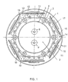
- the arrangement of the components of a converter according to the invention is schematic in a plan view in Fig. 1 and in a Side view and partially shown in section in FIG. 2.
- the illustrated embodiment is based on a three-phase Converter, the electrical circuit diagram of which is associated three-phase bridge circuit with the necessary semiconductor power components is shown in Fig. 3.
- a carrier 1 designed as a hollow body is provided with cooling channels 2 provided and on its inside 3 cylindrical and on its Outside 4 formed as a hexagon. This creates on the Outside 4 of the hollow body-shaped carrier 1 a substantially cylindrical shape.
- the hollow-shaped carrier 1 on one end face with a Carrier part 6 containing cooling channels 5 may be provided. Because of this Carrier part 6, the hollow body receives a pot-like shape and it the possibility is given by the support member 6 and its Cooling channels 5 the cooling channels contained in the wall of the carrier 1 2 to connect with each other.
- the cooling channels 2 in the hollow-shaped carriers 1 are suitably shaped and more suitable Place attached. In the example shown with the hexagonal shape, they are preferably in Edge area, where the wall thickness is somewhat larger, accommodated.
- the two connections 8 and 9 protrude for the positive and the negative pole. Otherwise, the condenser 7, except for this end face, is closely surrounded on all sides by the cup-shaped hollow body 1 serving as a carrier and is thus fully exposed to its cooling.
- the semiconductor power components 10 and 11 are each applied to one surface on the outside of the hollow body 1. 3 can be a transistor T1 and a diode D1 or T4 and D4 connected in parallel to it, which are assigned to a phase and are arranged on two adjacent surfaces.
- the transistors T1 and the diode D1 and the transistor T4 and the diode D4 connected in parallel thereto belong to the line 12 on the adjacent surface.
- These semiconductor power components are connected to a line, such as in particular a line 12, line 13 or line 14, each through a bus bar called 15.
- the second phase, which is brought out on line 13 includes the bridge part with the transistor T2 and the diode D2 and the transistor T5 and the diode associated with it D5.
- the third bridge part of the three-phase converter is assigned the transistor T3 with its diode D3 and the transistor T6 with its diode D6 on the line 14.
- the semiconductor power components assigned to each third of the bridge are thus arranged on one side of the line 12, 13 or 14 on the outer surfaces of the hollow body 1 lying symmetrically to these line connections and fastened in good heat-conducting contact on the corresponding flat surfaces of the carrier 1. This can be seen particularly well in the top view of FIG. 1.
- the direct current connection on lines 8 and 9 is brought to the semiconductor power components via a busbar 16, also known as a busbar, as is clearly shown in FIG. 2.
- Drive boards 17 are provided on each of the six surfaces directly the semiconductor power components underneath drive. These six control boards 17 are connected to a further board, the control board 18, either via connector 19 or flexible PCB connector 20, as shown on the left or right in FIG. 2 is shown. There is another circuit board 18 there shown for the purposes not relevant here in the Converter can be installed. This entire arrangement is from a cover 21, which in the illustrated case is cylindrical and all components except the Cable outlets 8, 9, 12, 13, 14 fully surrounded. With that one is built-in, self-contained and on the lines 8, 9, 12, 13 and 14 connectable component with a very compact packed converter.
- the cylindrical capacitor 7 is arranged at the center of the Hexagonal profile, which is cylindrical on the inside 3 is designed.
- the cylindrical capacitor 7 is arranged on each outer surface 4 of the hexagonal profile of the hollow body Carrier 1 .
- the half bridges are connected via busbar called connecting rails 15 and 16.
- the five Line connections 8, 9, 12, 13, 15 can be made at any suitable Position, be it radial or axial. in the illustrated example, they are axially together on one end face led out.
- the hollow body or cup-shaped carrier 1 is in its axial extent preferably designed as long as it is predetermined by the height of the necessary capacitor 7.
- the design of the outer surface of the hollow-shaped carrier can be made so that four External surfaces are provided, and on two adjacent ones External surfaces of the semiconductor power components that lead to a Half bridge belong, are arranged adjacent.
- the connection and Control with the respective elements is then similar to that in illustrated embodiment.
- Here is then used as a cover a cuboid cover used.
- the whole given the cuboid construction volume by the components optimal is used and not just a part.
- capacitor 7 instead of one centrally in hollow-shaped carrier 1 arranged capacitor 7 a Capacitor arrangement consisting of a series of capacitors in Parallel connection exists, can be used and centrally inside of the hollow body can be arranged. Then there is the The inside surface of the hollow-body-shaped carrier is optimally appropriate adapt the given shape and the cooling channels 2 to be provided accordingly in the most suitable places.
- the basic idea of the present invention is therefore to arrange the capacitor or capacitors centrally in a hollow body and on the outside of the hollow body, the necessary semiconductor components to arrange.
- the hollow body contains in its wall which flowed through in particular by a cooling liquid Cooling channels 2 in a suitable place and cools both the in well attached heat-conducting transition on the outside Semiconductor components as well as the one or more inside provided power capacitors.
Landscapes
- Engineering & Computer Science (AREA)
- Microelectronics & Electronic Packaging (AREA)
- Power Engineering (AREA)
- Physics & Mathematics (AREA)
- Thermal Sciences (AREA)
- Inverter Devices (AREA)
- Electric Propulsion And Braking For Vehicles (AREA)
Applications Claiming Priority (3)
| Application Number | Priority Date | Filing Date | Title |
|---|---|---|---|
| DE19846156 | 1998-10-07 | ||
| DE19846156A DE19846156C1 (de) | 1998-10-07 | 1998-10-07 | Anordnung eines mehrphasigen Umrichters |
| PCT/DE1999/003185 WO2000021187A1 (de) | 1998-10-07 | 1999-10-02 | Anordnung eines mehrphasigen umrichters |
Publications (2)
| Publication Number | Publication Date |
|---|---|
| EP1119899A1 EP1119899A1 (de) | 2001-08-01 |
| EP1119899B1 true EP1119899B1 (de) | 2002-10-02 |
Family
ID=7883676
Family Applications (1)
| Application Number | Title | Priority Date | Filing Date |
|---|---|---|---|
| EP99970217A Expired - Lifetime EP1119899B1 (de) | 1998-10-07 | 1999-10-02 | Anordnung eines mehrphasigen umrichters |
Country Status (5)
| Country | Link |
|---|---|
| US (1) | US6501653B1 (enExample) |
| EP (1) | EP1119899B1 (enExample) |
| JP (1) | JP2002528028A (enExample) |
| DE (2) | DE19846156C1 (enExample) |
| WO (1) | WO2000021187A1 (enExample) |
Families Citing this family (54)
| Publication number | Priority date | Publication date | Assignee | Title |
|---|---|---|---|---|
| US7180100B2 (en) * | 2001-03-27 | 2007-02-20 | Ricoh Company, Ltd. | Semiconductor light-emitting device, surface-emission laser diode, and production apparatus thereof, production method, optical module and optical telecommunication system |
| DE10123626A1 (de) * | 2001-05-15 | 2002-11-21 | Bosch Gmbh Robert | Umrichter für elektrische Maschinen |
| GB2381675B (en) * | 2001-10-31 | 2003-12-24 | Penny & Giles Drives Technolog | Electronic control arrangement |
| US7061775B2 (en) | 2002-01-16 | 2006-06-13 | Rockwell Automation Technologies, Inc. | Power converter having improved EMI shielding |
| US6982873B2 (en) * | 2002-01-16 | 2006-01-03 | Rockwell Automation Technologies, Inc. | Compact vehicle drive module having improved thermal control |
| US7187568B2 (en) | 2002-01-16 | 2007-03-06 | Rockwell Automation Technologies, Inc. | Power converter having improved terminal structure |
| US7142434B2 (en) * | 2002-01-16 | 2006-11-28 | Rockwell Automation Technologies, Inc. | Vehicle drive module having improved EMI shielding |
| US7177153B2 (en) | 2002-01-16 | 2007-02-13 | Rockwell Automation Technologies, Inc. | Vehicle drive module having improved cooling configuration |
| US6865080B2 (en) * | 2002-01-16 | 2005-03-08 | Rockwell Automation Technologies, Inc. | Compact fluid cooled power converter supporting multiple circuit boards |
| US7187548B2 (en) | 2002-01-16 | 2007-03-06 | Rockwell Automation Technologies, Inc. | Power converter having improved fluid cooling |
| US6972957B2 (en) * | 2002-01-16 | 2005-12-06 | Rockwell Automation Technologies, Inc. | Modular power converter having fluid cooled support |
| US7032695B2 (en) | 2002-01-16 | 2006-04-25 | Rockwell Automation Technologies, Inc. | Vehicle drive module having improved terminal design |
| US6898072B2 (en) | 2002-01-16 | 2005-05-24 | Rockwell Automation Technologies, Inc. | Cooled electrical terminal assembly and device incorporating same |
| US6909607B2 (en) | 2002-01-16 | 2005-06-21 | Rockwell Automation Technologies, Inc. | Thermally matched fluid cooled power converter |
| US6965514B2 (en) * | 2002-01-16 | 2005-11-15 | Rockwell Automation Technologies, Inc. | Fluid cooled vehicle drive module |
| DE10220047A1 (de) * | 2002-05-04 | 2003-11-20 | Jungheinrich Ag | Antriebssystem mit Umrichtersteuerung für Niederspannungs-Drehstrommotoren |
| JP3759097B2 (ja) * | 2002-10-24 | 2006-03-22 | ファナック株式会社 | 冷却ジャケット及び冷却ジャケットを装着した電動機 |
| DE10306227B4 (de) * | 2003-02-13 | 2009-01-02 | Sew-Eurodrive Gmbh & Co. Kg | Leistungsmodul und Umrichter |
| DE10326321A1 (de) | 2003-06-11 | 2005-01-13 | Compact Dynamics Gmbh | Elektronische Baugruppe zum Schalten elektrischer Leistung |
| US6778389B1 (en) * | 2003-07-03 | 2004-08-17 | Visteon Global Technologies, Inc. | Microelectronic package with tubular housing |
| US7180736B2 (en) * | 2003-07-10 | 2007-02-20 | Visteon Global Technologies, Inc. | Microelectronic package within cylindrical housing |
| US7129808B2 (en) * | 2004-09-01 | 2006-10-31 | Rockwell Automation Technologies, Inc. | Core cooling for electrical components |
| JP4106061B2 (ja) * | 2005-04-22 | 2008-06-25 | 三菱電機株式会社 | パワーユニット装置及び電力変換装置 |
| JP5205595B2 (ja) * | 2006-12-07 | 2013-06-05 | 日産自動車株式会社 | 電力変換装置およびモータ駆動システム |
| US7796388B2 (en) * | 2008-03-17 | 2010-09-14 | Ut-Battelle, Llc | Direct cooled power electronics substrate |
| DE102009024370B4 (de) * | 2009-06-09 | 2014-04-30 | Semikron Elektronik Gmbh & Co. Kg | Stromrichteranordnung mit Kühleinrichtung und Herstellungsverfahren hierzu |
| JP5062302B2 (ja) * | 2010-06-29 | 2012-10-31 | 株式会社デンソー | 冷却器への電子部品内蔵配線基板の取付構造及びその取付方法 |
| US8289711B2 (en) * | 2010-08-20 | 2012-10-16 | Hamilton Sundstrand Corporation | Integrated thermal packaging of high power motor controller |
| DE102011088250A1 (de) * | 2011-12-12 | 2013-06-13 | Robert Bosch Gmbh | Leistungsmodul für einen elektrischen Antrieb |
| JP5726215B2 (ja) * | 2013-01-11 | 2015-05-27 | 株式会社豊田中央研究所 | 冷却型スイッチング素子モジュール |
| EP2804306A1 (de) * | 2013-05-15 | 2014-11-19 | Siemens Aktiengesellschaft | Stromrichteranordnung und Verfahren zur Herstellung einer Stromrichteranordnung |
| JP6149611B2 (ja) * | 2013-08-29 | 2017-06-21 | アイシン・エィ・ダブリュ株式会社 | インバータ装置及び車両用駆動装置 |
| CN104734533B (zh) * | 2013-12-19 | 2018-01-12 | 联合汽车电子有限公司 | 紧凑型逆变器及其制造方法 |
| TWI539894B (zh) * | 2014-11-28 | 2016-06-21 | 財團法人工業技術研究院 | 功率模組 |
| DE112015006352T5 (de) * | 2015-03-25 | 2017-11-30 | Mitsubishi Electric Corporation | Energiewandlereinrichtung |
| EP3148303A1 (de) * | 2015-09-23 | 2017-03-29 | Siemens Aktiengesellschaft | Elektrische schaltungsanordnung mit kondensator mit gehäusefunktion |
| FR3056018B1 (fr) * | 2016-09-15 | 2018-11-23 | Alstom Transport Technologies | Module de puissance multi-faces |
| KR101936996B1 (ko) * | 2016-12-15 | 2019-01-09 | 현대자동차주식회사 | 모터용 3상 인버터 |
| FR3061627B1 (fr) * | 2016-12-29 | 2019-09-06 | Commissariat A L'energie Atomique Et Aux Energies Alternatives | Architecture d'un commutateur triphase |
| FR3068545B1 (fr) * | 2017-06-28 | 2019-07-19 | Valeo Equipements Electriques Moteur | Convertisseur de tension, systeme electrique, vehicule automobile et procede de fabrication associes |
| DE102017223631A1 (de) * | 2017-12-21 | 2019-06-27 | Robert Bosch Gmbh | Inverter für eine elektrische Maschine |
| FR3078456B1 (fr) * | 2018-02-27 | 2020-02-28 | Institut Vedecom | Module de commutation de puissance et dispositif electronique de puissance integrant celui-ci |
| FR3078448B1 (fr) * | 2018-02-27 | 2020-02-28 | Institut Vedecom | Ensemble de bus barres formant boitier et dissipateur thermique pour un dispositif electronique de puissance |
| JP7006486B2 (ja) * | 2018-04-25 | 2022-01-24 | 株式会社アイシン | 車両用駆動装置 |
| TWI672892B (zh) | 2018-06-22 | 2019-09-21 | 群光電能科技股份有限公司 | 馬達套筒及馬達裝置 |
| JP7202979B2 (ja) | 2019-06-13 | 2023-01-12 | 株式会社Soken | 電力変換装置 |
| DE102020200304A1 (de) * | 2020-01-13 | 2021-07-29 | Zf Friedrichshafen Ag | Dreiphasiger Wechselrichter |
| US12474751B2 (en) * | 2021-03-11 | 2025-11-18 | Core Scientific, Inc. | System for cooling circuit boards |
| CN113163677B (zh) * | 2021-03-25 | 2023-01-17 | 联想(北京)有限公司 | 一种电子设备 |
| DE102021213427B3 (de) | 2021-11-29 | 2023-05-25 | Zf Friedrichshafen Ag | Kompaktes leistungswechselrichtermodul |
| DE202022100279U1 (de) * | 2022-01-19 | 2023-04-21 | WAGO Verwaltungsgesellschaft mit beschränkter Haftung | Leiterplattenmontage |
| JP7849229B2 (ja) * | 2022-06-20 | 2026-04-21 | サンデン株式会社 | 電動圧縮機 |
| DE112024001446T5 (de) * | 2023-03-28 | 2026-01-08 | Rohm Co., Ltd. | Halbleitermodul und fahrzeug |
| US20250267824A1 (en) | 2024-02-16 | 2025-08-21 | Caterpillar Inc. | Packaged power inverter |
Family Cites Families (11)
| Publication number | Priority date | Publication date | Assignee | Title |
|---|---|---|---|---|
| US4538025A (en) * | 1984-01-16 | 1985-08-27 | Emhart Industries, Inc. | Anchoring apparatus for a capacitor |
| US4581695A (en) * | 1984-12-12 | 1986-04-08 | Sundstrand Corporation | Rectifier assembly |
| DE4000303A1 (de) * | 1990-01-08 | 1991-07-11 | Technology Service Inc | Versorgungsschaltung zur strom- bzw. spannungsversorgung elektronischer geraete od.dgl. |
| JP2536657B2 (ja) * | 1990-03-28 | 1996-09-18 | 三菱電機株式会社 | 電気装置及びその製造方法 |
| WO1992019013A1 (en) * | 1991-04-16 | 1992-10-29 | Arthur Iversen | Power semiconductor packaging |
| DE4412990A1 (de) * | 1994-04-15 | 1995-10-19 | Abb Patent Gmbh | Stromrichteranlage mit flüssigkeits- oder luftgekühlten Leistungshalbleitern und Gleichspannungszwischenkreis |
| JP3346039B2 (ja) * | 1994-08-08 | 2002-11-18 | トヨタ自動車株式会社 | インバータ一体型電動機 |
| US5648892A (en) * | 1995-09-29 | 1997-07-15 | Allen-Bradley Company, Inc. | Wireless circuit board system for a motor controller |
| JP3159071B2 (ja) * | 1996-08-01 | 2001-04-23 | 株式会社日立製作所 | 放熱フィンを有する電気装置 |
| DE19645636C1 (de) * | 1996-11-06 | 1998-03-12 | Telefunken Microelectron | Leistungsmodul zur Ansteuerung von Elektromotoren |
| US5914860A (en) | 1998-01-20 | 1999-06-22 | Reliance Electric Industrial Company | Small volume heat sink/electronic assembly |
-
1998
- 1998-10-07 DE DE19846156A patent/DE19846156C1/de not_active Expired - Fee Related
-
1999
- 1999-10-02 WO PCT/DE1999/003185 patent/WO2000021187A1/de not_active Ceased
- 1999-10-02 US US09/807,157 patent/US6501653B1/en not_active Expired - Fee Related
- 1999-10-02 DE DE59902974T patent/DE59902974D1/de not_active Expired - Fee Related
- 1999-10-02 EP EP99970217A patent/EP1119899B1/de not_active Expired - Lifetime
- 1999-10-02 JP JP2000575209A patent/JP2002528028A/ja active Pending
Also Published As
| Publication number | Publication date |
|---|---|
| DE19846156C1 (de) | 2000-07-27 |
| EP1119899A1 (de) | 2001-08-01 |
| WO2000021187A1 (de) | 2000-04-13 |
| DE59902974D1 (de) | 2002-11-07 |
| JP2002528028A (ja) | 2002-08-27 |
| US6501653B1 (en) | 2002-12-31 |
Similar Documents
| Publication | Publication Date | Title |
|---|---|---|
| EP1119899B1 (de) | Anordnung eines mehrphasigen umrichters | |
| EP1359662B1 (de) | Antriebssystem mit Umrichtersteuerung für Niederspannungs-Drehstrommotoren | |
| DE4110339C3 (de) | Wechselrichter mit plattenförmigen Gleichspannungszuleitungen | |
| EP3632197B1 (de) | Leistungsphasenmodul eines umrichters, umrichter, und fahrzeug | |
| EP3605762B1 (de) | Anordnung mit einer stromschienenvorrichtung und einem stromrichtergehäuse sowie verfahren zu deren herstellung, stromrichter für ein fahrzeug und fahrzeug | |
| DE102016207701B4 (de) | Leistungsumsetzer und Schienenfahrzeuge | |
| DE102019133377B4 (de) | Wechselrichter mit kompakter bauform | |
| EP2996449B1 (de) | Stromrichteranordnung mit einem mehrphasigen Stromrichter | |
| DE19845821B4 (de) | Stromrichtereinheit in Modulbauweise, insbesondere für Schienenfahrzeuge | |
| DE10303253A1 (de) | Elektrische Energieverteilereinheit für ein elektrisches Verbindergehäuse, sowie zugehöriges elektrisches Verbindergehäuse | |
| AT521040B1 (de) | Leistungsbaugruppe mit tragendem Kühlkörper | |
| DE102018202479A1 (de) | Kühlkörper für Leistungselektronikanordnung | |
| EP0677916B1 (de) | Stromrichteranlage mit flüssigkeits- oder luftgekühlten Leistungshalbleitern und Gleichspannungszwischenkreis | |
| DE2426229A1 (de) | Traeger fuer den phasenaufbau eines wechselrichters | |
| DE102022206596B4 (de) | Einzelphasenmodul eines Inverters, Inverter und Leistungselektronik | |
| DE10302371A1 (de) | Elektrische Energieverteilereinheit für ein elektrisches Verbindergehäuse, sowie Verbindergehäuse hiermit | |
| EP0994557B1 (de) | Umrichter mit niederinduktivem Kondensator im Zwischenkreis | |
| EP1125355B1 (de) | Kondensatorbaugruppe für ein stromrichtergerät | |
| DE4338277C2 (de) | Flüssigkeitsgekühltes Stromrichtermodul mit Beschaltungsbauelementen für abschaltbare Leistungshalbleiter | |
| DE102022206604B4 (de) | Einzelphasenmodul eines Inverters, Inverter und Leistungselektronik | |
| DE102008009913A1 (de) | Stromrichtermodul der Leistungselektronik | |
| DE3920686C2 (de) | Stromschienen-Leiterplatte | |
| DE19734270B4 (de) | Luftgekühltes Stromrichtermodul | |
| DE19850153B4 (de) | Halbleiter-Schaltungsanordnung, insbesondere Hochstromumrichter mit niedriger Zwischenkreisspannung | |
| DE102022123261B4 (de) | Leistungselektronische Baugruppe mit einem Gehäuse und mit einer darin angeordneten Kondensatoreinrichtung |
Legal Events
| Date | Code | Title | Description |
|---|---|---|---|
| PUAI | Public reference made under article 153(3) epc to a published international application that has entered the european phase |
Free format text: ORIGINAL CODE: 0009012 |
|
| 17P | Request for examination filed |
Effective date: 20010507 |
|
| AK | Designated contracting states |
Kind code of ref document: A1 Designated state(s): AT BE CH CY DE DK ES FI FR GB GR IE IT LI LU MC NL PT SE |
|
| GRAG | Despatch of communication of intention to grant |
Free format text: ORIGINAL CODE: EPIDOS AGRA |
|
| 17Q | First examination report despatched |
Effective date: 20011210 |
|
| GRAG | Despatch of communication of intention to grant |
Free format text: ORIGINAL CODE: EPIDOS AGRA |
|
| GRAH | Despatch of communication of intention to grant a patent |
Free format text: ORIGINAL CODE: EPIDOS IGRA |
|
| GRAH | Despatch of communication of intention to grant a patent |
Free format text: ORIGINAL CODE: EPIDOS IGRA |
|
| GRAA | (expected) grant |
Free format text: ORIGINAL CODE: 0009210 |
|
| AK | Designated contracting states |
Kind code of ref document: B1 Designated state(s): DE ES FR GB IT |
|
| PG25 | Lapsed in a contracting state [announced via postgrant information from national office to epo] |
Ref country code: IT Free format text: LAPSE BECAUSE OF FAILURE TO SUBMIT A TRANSLATION OF THE DESCRIPTION OR TO PAY THE FEE WITHIN THE PRESCRIBED TIME-LIMIT;WARNING: LAPSES OF ITALIAN PATENTS WITH EFFECTIVE DATE BEFORE 2007 MAY HAVE OCCURRED AT ANY TIME BEFORE 2007. THE CORRECT EFFECTIVE DATE MAY BE DIFFERENT FROM THE ONE RECORDED. Effective date: 20021002 |
|
| REG | Reference to a national code |
Ref country code: GB Ref legal event code: FG4D Free format text: NOT ENGLISH |
|
| REG | Reference to a national code |
Ref country code: IE Ref legal event code: FG4D Free format text: GERMAN |
|
| REF | Corresponds to: |
Ref document number: 59902974 Country of ref document: DE Date of ref document: 20021107 |
|
| GBT | Gb: translation of ep patent filed (gb section 77(6)(a)/1977) |
Effective date: 20030212 |
|
| ET | Fr: translation filed | ||
| PG25 | Lapsed in a contracting state [announced via postgrant information from national office to epo] |
Ref country code: ES Free format text: LAPSE BECAUSE OF FAILURE TO SUBMIT A TRANSLATION OF THE DESCRIPTION OR TO PAY THE FEE WITHIN THE PRESCRIBED TIME-LIMIT Effective date: 20030429 |
|
| REG | Reference to a national code |
Ref country code: IE Ref legal event code: FD4D Ref document number: 1119899E Country of ref document: IE |
|
| PLBE | No opposition filed within time limit |
Free format text: ORIGINAL CODE: 0009261 |
|
| STAA | Information on the status of an ep patent application or granted ep patent |
Free format text: STATUS: NO OPPOSITION FILED WITHIN TIME LIMIT |
|
| 26N | No opposition filed |
Effective date: 20030703 |
|
| PGFP | Annual fee paid to national office [announced via postgrant information from national office to epo] |
Ref country code: DE Payment date: 20081222 Year of fee payment: 10 |
|
| PGFP | Annual fee paid to national office [announced via postgrant information from national office to epo] |
Ref country code: GB Payment date: 20091023 Year of fee payment: 11 Ref country code: FR Payment date: 20091110 Year of fee payment: 11 |
|
| PG25 | Lapsed in a contracting state [announced via postgrant information from national office to epo] |
Ref country code: DE Free format text: LAPSE BECAUSE OF NON-PAYMENT OF DUE FEES Effective date: 20100501 |
|
| GBPC | Gb: european patent ceased through non-payment of renewal fee |
Effective date: 20101002 |
|
| PG25 | Lapsed in a contracting state [announced via postgrant information from national office to epo] |
Ref country code: FR Free format text: LAPSE BECAUSE OF NON-PAYMENT OF DUE FEES Effective date: 20101102 |
|
| REG | Reference to a national code |
Ref country code: FR Ref legal event code: ST Effective date: 20110630 |
|
| PG25 | Lapsed in a contracting state [announced via postgrant information from national office to epo] |
Ref country code: GB Free format text: LAPSE BECAUSE OF NON-PAYMENT OF DUE FEES Effective date: 20101002 |