EP1111687B1 - Dispositif semi-conducteur MOS - Google Patents
Dispositif semi-conducteur MOS Download PDFInfo
- Publication number
- EP1111687B1 EP1111687B1 EP00128104A EP00128104A EP1111687B1 EP 1111687 B1 EP1111687 B1 EP 1111687B1 EP 00128104 A EP00128104 A EP 00128104A EP 00128104 A EP00128104 A EP 00128104A EP 1111687 B1 EP1111687 B1 EP 1111687B1
- Authority
- EP
- European Patent Office
- Prior art keywords
- region
- type
- semiconductor layer
- drift region
- impurity concentration
- Prior art date
- Legal status (The legal status is an assumption and is not a legal conclusion. Google has not performed a legal analysis and makes no representation as to the accuracy of the status listed.)
- Expired - Lifetime
Links
- 239000004065 semiconductor Substances 0.000 title claims description 111
- 239000012535 impurity Substances 0.000 claims description 116
- 230000003247 decreasing effect Effects 0.000 claims description 20
- 239000000758 substrate Substances 0.000 claims description 13
- 239000010410 layer Substances 0.000 description 117
- 230000007423 decrease Effects 0.000 description 16
- 238000010438 heat treatment Methods 0.000 description 10
- 238000004519 manufacturing process Methods 0.000 description 10
- VYPSYNLAJGMNEJ-UHFFFAOYSA-N Silicium dioxide Chemical compound O=[Si]=O VYPSYNLAJGMNEJ-UHFFFAOYSA-N 0.000 description 9
- 238000009792 diffusion process Methods 0.000 description 9
- 238000000034 method Methods 0.000 description 9
- 229910052814 silicon oxide Inorganic materials 0.000 description 9
- 230000005684 electric field Effects 0.000 description 6
- 229910021421 monocrystalline silicon Inorganic materials 0.000 description 6
- 230000000694 effects Effects 0.000 description 4
- 238000002474 experimental method Methods 0.000 description 4
- 238000010276 construction Methods 0.000 description 3
- 238000012545 processing Methods 0.000 description 3
- 239000000969 carrier Substances 0.000 description 2
- 238000005530 etching Methods 0.000 description 2
- 229910021420 polycrystalline silicon Inorganic materials 0.000 description 2
- 239000011241 protective layer Substances 0.000 description 2
- 230000015556 catabolic process Effects 0.000 description 1
- 238000013461 design Methods 0.000 description 1
- 239000012212 insulator Substances 0.000 description 1
- 238000012986 modification Methods 0.000 description 1
- 230000004048 modification Effects 0.000 description 1
- 238000000059 patterning Methods 0.000 description 1
- 229920006395 saturated elastomer Polymers 0.000 description 1
- 238000012360 testing method Methods 0.000 description 1
Images


Classifications
-
- H—ELECTRICITY
- H01—ELECTRIC ELEMENTS
- H01L—SEMICONDUCTOR DEVICES NOT COVERED BY CLASS H10
- H01L29/00—Semiconductor devices specially adapted for rectifying, amplifying, oscillating or switching and having potential barriers; Capacitors or resistors having potential barriers, e.g. a PN-junction depletion layer or carrier concentration layer; Details of semiconductor bodies or of electrodes thereof ; Multistep manufacturing processes therefor
- H01L29/66—Types of semiconductor device ; Multistep manufacturing processes therefor
- H01L29/68—Types of semiconductor device ; Multistep manufacturing processes therefor controllable by only the electric current supplied, or only the electric potential applied, to an electrode which does not carry the current to be rectified, amplified or switched
- H01L29/76—Unipolar devices, e.g. field effect transistors
- H01L29/772—Field effect transistors
- H01L29/78—Field effect transistors with field effect produced by an insulated gate
- H01L29/7801—DMOS transistors, i.e. MISFETs with a channel accommodating body or base region adjoining a drain drift region
- H01L29/7816—Lateral DMOS transistors, i.e. LDMOS transistors
- H01L29/7824—Lateral DMOS transistors, i.e. LDMOS transistors with a substrate comprising an insulating layer, e.g. SOI-LDMOS transistors
-
- H—ELECTRICITY
- H01—ELECTRIC ELEMENTS
- H01L—SEMICONDUCTOR DEVICES NOT COVERED BY CLASS H10
- H01L29/00—Semiconductor devices specially adapted for rectifying, amplifying, oscillating or switching and having potential barriers; Capacitors or resistors having potential barriers, e.g. a PN-junction depletion layer or carrier concentration layer; Details of semiconductor bodies or of electrodes thereof ; Multistep manufacturing processes therefor
- H01L29/02—Semiconductor bodies ; Multistep manufacturing processes therefor
- H01L29/06—Semiconductor bodies ; Multistep manufacturing processes therefor characterised by their shape; characterised by the shapes, relative sizes, or dispositions of the semiconductor regions ; characterised by the concentration or distribution of impurities within semiconductor regions
- H01L29/08—Semiconductor bodies ; Multistep manufacturing processes therefor characterised by their shape; characterised by the shapes, relative sizes, or dispositions of the semiconductor regions ; characterised by the concentration or distribution of impurities within semiconductor regions with semiconductor regions connected to an electrode carrying current to be rectified, amplified or switched and such electrode being part of a semiconductor device which comprises three or more electrodes
- H01L29/0843—Source or drain regions of field-effect devices
- H01L29/0847—Source or drain regions of field-effect devices of field-effect transistors with insulated gate
- H01L29/0852—Source or drain regions of field-effect devices of field-effect transistors with insulated gate of DMOS transistors
- H01L29/0873—Drain regions
- H01L29/0878—Impurity concentration or distribution
-
- H—ELECTRICITY
- H01—ELECTRIC ELEMENTS
- H01L—SEMICONDUCTOR DEVICES NOT COVERED BY CLASS H10
- H01L29/00—Semiconductor devices specially adapted for rectifying, amplifying, oscillating or switching and having potential barriers; Capacitors or resistors having potential barriers, e.g. a PN-junction depletion layer or carrier concentration layer; Details of semiconductor bodies or of electrodes thereof ; Multistep manufacturing processes therefor
- H01L29/66—Types of semiconductor device ; Multistep manufacturing processes therefor
- H01L29/66007—Multistep manufacturing processes
- H01L29/66075—Multistep manufacturing processes of devices having semiconductor bodies comprising group 14 or group 13/15 materials
- H01L29/66227—Multistep manufacturing processes of devices having semiconductor bodies comprising group 14 or group 13/15 materials the devices being controllable only by the electric current supplied or the electric potential applied, to an electrode which does not carry the current to be rectified, amplified or switched, e.g. three-terminal devices
- H01L29/66409—Unipolar field-effect transistors
- H01L29/66477—Unipolar field-effect transistors with an insulated gate, i.e. MISFET
- H01L29/66674—DMOS transistors, i.e. MISFETs with a channel accommodating body or base region adjoining a drain drift region
- H01L29/66681—Lateral DMOS transistors, i.e. LDMOS transistors
-
- H—ELECTRICITY
- H01—ELECTRIC ELEMENTS
- H01L—SEMICONDUCTOR DEVICES NOT COVERED BY CLASS H10
- H01L29/00—Semiconductor devices specially adapted for rectifying, amplifying, oscillating or switching and having potential barriers; Capacitors or resistors having potential barriers, e.g. a PN-junction depletion layer or carrier concentration layer; Details of semiconductor bodies or of electrodes thereof ; Multistep manufacturing processes therefor
- H01L29/66—Types of semiconductor device ; Multistep manufacturing processes therefor
- H01L29/68—Types of semiconductor device ; Multistep manufacturing processes therefor controllable by only the electric current supplied, or only the electric potential applied, to an electrode which does not carry the current to be rectified, amplified or switched
- H01L29/76—Unipolar devices, e.g. field effect transistors
- H01L29/772—Field effect transistors
- H01L29/78—Field effect transistors with field effect produced by an insulated gate
- H01L29/786—Thin film transistors, i.e. transistors with a channel being at least partly a thin film
- H01L29/78606—Thin film transistors, i.e. transistors with a channel being at least partly a thin film with supplementary region or layer in the thin film or in the insulated bulk substrate supporting it for controlling or increasing the safety of the device
- H01L29/78618—Thin film transistors, i.e. transistors with a channel being at least partly a thin film with supplementary region or layer in the thin film or in the insulated bulk substrate supporting it for controlling or increasing the safety of the device characterised by the drain or the source properties, e.g. the doping structure, the composition, the sectional shape or the contact structure
- H01L29/78621—Thin film transistors, i.e. transistors with a channel being at least partly a thin film with supplementary region or layer in the thin film or in the insulated bulk substrate supporting it for controlling or increasing the safety of the device characterised by the drain or the source properties, e.g. the doping structure, the composition, the sectional shape or the contact structure with LDD structure or an extension or an offset region or characterised by the doping profile
- H01L29/78624—Thin film transistors, i.e. transistors with a channel being at least partly a thin film with supplementary region or layer in the thin film or in the insulated bulk substrate supporting it for controlling or increasing the safety of the device characterised by the drain or the source properties, e.g. the doping structure, the composition, the sectional shape or the contact structure with LDD structure or an extension or an offset region or characterised by the doping profile the source and the drain regions being asymmetrical
Definitions
- the present invention relates to a semiconductor device for use as a switching element.
- SOI silicon-on-insulator
- LDMOSFET lateral double-diffused MOSFET
- a conventional SOI-LDMOSFET is constructed as follows, using a SOI substrate which comprises a semiconductor substrate (1) formed from a single crystal silicon, an insulating layer (2) formed from a silicon oxide on the semiconductor substrate (1), and a semiconductor layer (3) formed from a single crystal silicon on the insulating layer (2) (see Fig. 10A )).
- a p + -type well region (5) and an n ++ -type drain region (4) are formed with a space therebetween in the n-type semiconductor layer (3), and an n ++ -type source region (6) is further formed in the p + -type well region (5).
- a part of the p + -type well region (5) and the n-type semiconductor layer (3) are located between the n ++ -type source region (6) and the n ++ -type drain region (4).
- a gate electrode (9) is formed from, for example, a poly-silicon, which is disposed on a gate-insulating layer (8) formed on the p + -type well region (5) between the n ++ -type source region (6) and the n ++ -type drain region (4).
- the gate electrode (9) is formed overhanging the n ++ -type source region (6) and the drift region located between the p + -type well region (5) and the n ++ -type drain region (4) in the n-type semiconductor layer (3), respectively, taken into account margins for a shift of the position in the process of production.
- a source electrode (11) and a drain electrode (10) are formed on the n ++ -type source region (6) and the n ++ -type drain region (4), respectively.
- the p + -type well region (5) turns into the original p-type layer, so that a PN junction in reverse bias is formed between the p + -type well region and the n ++ -type drain region (4).
- current does not flow between the n + ⁇ -type source region (6) and the n ++ -type drain region (4).
- drift region (20) a part of the n-type semiconductor layer (3) between the p + -type well region (5) forming the channel and the n ++ -type drain region (4) is called a drift region (20), and the impurity concentration NO of the drift region (20) is so selected as to satisfy the RESURF condition expressed by the following equation (1).
- Tsoi X NO ⁇ 1 X 10 12 atm / cm 2 wherein Tsoi represents the thickness of the drift region.
- the conventional SOI-LDMOSFET achieves high withstand voltage by selecting the impurity concentration NO of the drift region (20) so that the above RESURF condition for providing optimal conditions relative to a surface electric field can be satisfied.
- the impurity concentration NO of the drift region (20) is so selected as to be uniform over a whole of the drift region (20).
- the n-type drift region (50) locates between the drain region (52) having the drain electrode (56) formed thereon and the source region (51) having the source electrode (54) formed thereon as shown in Fig. 11 , and the drift region (50) is so formed that the impurity concentration of the drift region (50) can linearly decrease as the distance from the drain region (52) increases.
- a space between the source region (51) and the drift region (50) has a gate electrode (59) formed therein spaced by the gate oxide layer (58) and a p-type base region (60) for forming a channel. Constructed as above, the SOI-LDMOSFET disclosed in U.S. Patent No. 5300448 succeeds in uniforming the surface and the internal electric field of the drift region (50) and thus further improving the withstand voltage.
- the SOI-LDMOSFET disclosed in U.S. Patent No. 5300448 has a problem in that it is impossible to decrease the length of the drift region (50) (the length along which current flows).
- This disadvantage comes from the following structure: as shown in Fig. 12 , the drift region is formed on the semiconductor layer (3) through a mask having a plurality of openings (40) which are formed so that the distance between each of the openings changes in order and such a semiconductor layer (3) is doped with a predetermined amount of impurity and then treated by heating, so that the impurity concentration of the drift region (50) changes in order.
- This structure makes it hard to shorten the length of the drift region (50). It is described in U.S. Patent No. 5300448 that the length of the drift region (50) is 40 to 50 ⁇ m.
- the SOI-LDMOSFET proposed in U.S. Patent No. 5300448 has a further problem in that it is inevitably needed to decrease the thickness of the drift region (50) in order to improve the withstand voltage, which leads to poor heat release. This results in a problem that allowable current in the state of ON can not be increased.
- the SOI-LDMOSFET proposed in U.S. Patent No. 5412241 provides the structure which makes it possible to decrease the on-state resistance and to improve the withstand voltage characteristics.
- this SOI-LDMOSFET has a gate-field plate structure and therefore has a problem in that the output capacitance is large.
- the switch for turning a high frequency signal on or off is keenly demanded in the voltage class from 20 to 300 V.
- a SOI-LDMOS of this class is constructed so as to have an ideal structural parameter, it is estimated that the optimal value of the length of the drift region is 1 to 15 ⁇ m.
- the present invention is made to overcome the foregoing problems, and the first object of the present invention is to provide a semiconductor device capable of increasing allowable current in the state of ON while ensuring the demanded withstand voltage and decreasing output capacitance and on-state resistance.
- a semiconductor device comprising a semiconductor layer formed on a semiconductor substrate, and the semiconductor layer includes
- a depletion layer is effectively spread in a part of the drift region in contact with the well region, so that the concentration of an electric field can be prevented and that high withstand voltage can be achieved. Further, since the semiconductor layer can be formed with a relative large thickness, the thermal resistance can be decreased, and thus, the allowable current in the state of ON can be increased.
- the impurity concentration of said first part of the drift region is lower than the impurity concentration N(RESURF) which satisfies the RESURF condition.
- the on-state resistance can be held lower, and the output capacitance can be effectively decreased.
- the semiconductor layer is formed on an insulating layer on the semiconductor substrate.
- the impurity concentration in the lateral direction of the drift region changes obeying the Gaussian distribution having, as a parameter, the distane x from the drain region in the lateral direction
- the impurity concentration in the vertical direction of the drift region changes obeying the Gaussian distribution having, as a parameter, the distance y from the drain region in the vertical direction.
- the impurity concentration distribution in the drift region can be controlled by the diffusion from the side of the drain region in the course of constructing the semiconductor device, so that the semiconductor device can be readily formed with high accuracy.
- a semiconductor device capable of having withstand voltage of 20 to 300 V class which is widely demanded for switches for turning high frequency signals on or off, and having a drift length of about 1 to about 15 ⁇ m can be easily constructed.
- the impurity concentration of a second part of the drift region in the vicinity of the drain region is higher than the impurity concentration N(RESURF) which satisfies the RESURF condition.
- the on-state resistance can be decreased.
- the RESURF condition referred to herein is to satisfy the following equation. Tsoi X N RESURF ⁇ 1 X 10 12 atm / cm 2
- the thickness t of the semiconductor layer is set within a rang of 0.3 ⁇ m ⁇ to ⁇ 15 ⁇ m.
- the resultant semiconductor device as a switching element can have withstand voltage of 25 to 100 V class and show excellent high frequency wave characteristics.
- the resultant semiconductor device as a switching element can have withstand voltage of 25 to 50 V class and show excellent high frequency wave characteristics.
- the lateral distance of the drift region from one end of the drain region to one end of the well region is set 15 ⁇ m or less. By doing so, the on-state resistance can be decreased. Further, by doing so, the impurity concentration distribution can be formed in practical time by the diffusion from the side of the drain region.
- the semiconductor device may be constructed by the following process.
- the process comprises the steps of separately forming a first conductivity type-drain region and a first conductivity type-source region apart from each other, forming a drift region between the drain region and the source region and in contact with the drain region, and forming a channel region in contact with the source region.
- the process further comprises the steps of doping a region for forming the drain region with a first conductivity type-impurity, and heating and diffusing the impurity in the drift region.
- the introduction of the impurity into the drain region and the introduction of the impurity into the drift region can be carried out, using the same mask window, so that the semiconductor device can be readily constructed easilly with high accuracy.
- n-type and the p-type conductivities may be replaced with each other.
- a LDMOSFET may be formed on an epitaxial wafer.
- a SOI-LDMOSFET according to this embodiment is constructed as follows, using a SOI substrate which comprises a semiconductor substrate (1) formed from a single crystal silicon, an insulating layer (2) formed thereon from a silicon oxide, and a semiconductor layer (3) formed thereon from a single crystal silicon.
- such a p + -type well region (105) that has a depth reaching the insulating layer (2) is formed at a predetermined position in the n-type semiconductor layer (3), and an n ++ -type drain region (104) is formed apart from the p + -type well region (105).
- n ++ -type source region (106) is formed in the p + -type well region (105), and a p ++ -type base contact region (107) is formed in adjacent to the n ++ -type source region (106).
- the p + -type well region (105) having a channel region (150) formed thereon and the n-type semiconductor layer (3) (the drift region (112)) are located between the n ++ -type source region (106) and the n ++ -type drain region (104).
- a gate electrode (109) of, for example, a poly-silicon is formed on a gate-insulating layer (108) which is formed on the p + -type well region (105) (or the channel region (150)) between the n ++ -type source region (106) and the n ++ -type drain region (104).
- n-type drift region (112) a part of the n-type semiconductor layer (3) between the p + -type well region (105) forming the channel region (150) formed thereon just under the gate electrode and the n ++ -type drain region (104) is referred to as an n-type drift region (112).
- the gate electrode (109) is formed overhanging the n-type drift region (112) by a predetermined length, and this portion overhanging the n-type drift region (112) is referred to as a gate overhanging region (113), and the length of such a portion is referred to as a gate overhanging length.
- a drain electrode (110) is formed on the n ++ -type drain region (104), and a source electrode (111) is formed on and across the n ++ -type source region (106) and the p ++ -type base contact region (107).
- the SOI-LDMOSFET constructed as above according to the first embodiment shown in Fig. 1A can turn current on or off between the drain region and the source region depending on a voltage applied to the gate electrode in the same manner as in the conventional SOI-LDMOSFET, and further can have superior characteristics described later to the conventional one, by constructing the n-type drift region (112) as follows.
- the impurity concentration of the n-type drift region (112) is adjusted to gradually decrease in both of the vertical direction (the thickness direction of the semiconductor layer, which is perpendicular to the top surface of the semiconductor layer) and the lateral direction (the direction parallel to the top surface of the semiconductor layer) as the distance from the n ++ -type drain region (104) increases, as shown in Figs. 1B and 1C .
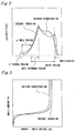
- Fig. 1B is a graph showing the impurity concentration distribution in the vicinity of the surface of the n-type drift region (112) in the lateral direction, and indicating the impurity concentration of a part of the surface of the n-type drift region (112) relative to the distance X from the reference point (the interface between the n-type drift region (112) and the n ++ -type drain region (104)) in the lateral direction.
- Fig. 1C is a graph showing the impurity concentration of the n-type drift region (112) relative to the distance Y from the surface of the semiconductor layer (3) in the depth direction (the vertical direction).
- the impurity concentration of the n-type drift region (112) is adjusted to gradually decrease toward the p + -type well region (105) from the n ++ -type drain region (104).
- the electric field concentrated around the region which is defined by the drift region beneath the gate overhanging region is relieved to form a more uniform electric field distribution in the n-type drift region (112).
- the SOI-LDMOSFET of the first embodiment can have higher avalanche breakdown point as shown in Fig. 3 .
- the impurity concentration of a part of the n-type drift region (112) in the vicinity of the junction between the p + -type well region (105) and the n-type drift region (112) is adjusted to be lower, and particularly, the impurity concentration is adjusted to be as low as the initial concentration level of the n-type semiconductor layer (3) in the vicinity of the insulating layer (2).
- a depletion layer is effectively spread from the junction between the p + -type well region (105) and the n-type drift region (112) toward the n ++ -type drain region (104) within the n-type drift region (112).
- the impurity concentration can be changed in not only the lateral direction but also the vertical direction, it is possible to form the n-type drift region (112) with a relatively large thickness.
- the increasing thickness of the drift region makes it possible to decrease the thermal resistance efficiently, so that allowable current in the state of ON can be increased. Therefore, the SOI-LDMOSFET can permit a relatively large amount of current to pass through in the state of ON.
- the SOI-LDMOSFET (100) of the first embodiment can have withstand voltage closer to an ideal value and also increase the amount of allowable current in the state of ON.
- the impurity concentration of a region (under gate overhanging region) located under the gate overhanging region (113) within the n-type drift region (112) is adjusted to be lower than the impurity concentration N(RESURF) which satisfies RESURF condition given by the following equation (3).
- N(RESURF) which satisfies RESURF condition given by the following equation (3).
- a depletion layer can be more effectively spread in the n-type drift region (112) in the state of OFF where the gate voltage is negative or at zero potential.
- RESURF the impurity concentration of the under gate overhanging region of the n-type drift region (112)
- the carrier concentration in the state of ON can be relatively high as in the case where the impurity concentration is set at a value equal to or greater than the value of N (RESURF), in spite of the condition under which the impurity concentration of the above region is set at a low value (less than N(RESURF)).
- the impurity concentration of the n-type drift region (112) is so adjusted as to change obeying the Gaussian distribution represented by the following equation (2).
- This impurity concentration distribution of the n-type drift region (112) which changes obeying the Gaussian distribution is determined by the distance from the end of the n ++ -type drain region (104) as the reference point, and therefore, the impurity concentration distribution of the n-type drift region (112) can be controlled by the diffusion from the side of the n ++ -type drain region (104).
- the n-type drift region (112) having the impurity concentration distribution which changes obeying the Gaussian distribution is not required to be subjected to highly accurate mask-processing which is essential for the construction of the conventional SOI-LDMOSFET, and therefore, it is readily formed.
- the SOI-LDMOSFET can have a short drift length.
- the use of the n-type drift region (112) having the impurity concentration distribution which changes obeying the Gaussian distribution makes it easy to construct a highly accurate SOI-LDMOSFET capable of having withstand voltage of 20 to 300 V class which is well required for a switch for turning a high frequency signal on or off and capable of having a drift length of about 1 to about 15 ⁇ m.
- the impurity concentration of a part of the n-type drift region (112) in the vicinity of the n ++ -type drain region (104) and also in the vicinity of the surface of the n-type drift region (112) (high concentration region) should be selected to a value higher than the impurity concentration N(RESURF) which satisfies the above RESURF condition.
- the carrier concentration in such a high impurity concentration region naturally becomes higher.
- Most of current which flows in the state of ON flows in the vicinity of the surface of the n-type drift region.
- the on state resistance can be decreased.
- the output capacitance can be suppressed without an increase in the on state resistance, by adjusting the impurity concentration of the part of the n-type drift region (112) just under the gate overhanging region (113) to a value lower than N(RESURF).
- the allowable current in the state of ON can be increased while the ideal withstand voltage being ensured, and also, the on-state resistance can be effectively decreased without an increase in the output capacitance.
- This process relates to a case where an impurity concentration distribution obeying the Gaussian distribution is formed in the n-type drift region.
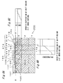
- an oxide layer is formed on the surface of a SOI substrate which comprises a substrate (1) formed from a single crystal silicon or the like, an insulating layer (2) formed thereon from a silicon oxide or the like, and a semiconductor layer (3) formed thereon from a single crystal silicon or the like.
- an oxide layer (1015) is formed by removing parts of the above oxide layer into which impurities will be doped to form a p + -type well region, an n ++ -type drain region and so on (see Fig. 7A ).
- n-type impurity is implanted into that region above (see Fig. 7B ).
- the n-type impurity is diffused by heat treatment so as to have a predetermined diffusion length.
- An impurity diffusion distribution obeying the Gaussian distribution represented by the equation (2) is formed in the n-type drift region (112) by controlling the temperature and the time of the heat treatment step.
- the pattern of this distribution is shown by the plurality of lines on Figs. 1 and 7C which are contour lines, and thus, in practice, the impurity concentration continuously changes according to the equation (2).
- an impurity for forming a p + -type well region (106) is implanted through the oxide layer (1015) as a mask and a resist mask (1017), and the impurity is diffused by heating so as to form the p + -type well region (106) which reaches up to the insulating layer (2).
- a resist mask (1018) for forming the n ++ -type source region (106) and the n ++ -type drain region (104) is formed, and an n-type impurity is implanted through the resist mask (1018) and the silicon oxide layer (1015) as a mask to thereby form n-type impurity-implanted regions (106a) and (104a) (see Fig. 7D ).
- the resist mask (1018) is removed, and then, a resist mask (1019) for forming a p ++ -type base contact region is formed, and a p-type impurity is introduced through the mask to form a p-type impurity-implanted region (107a) (see Fig. 7E ).
- heat treatment is carried out so as to diffuse the respective impurities in the n-type impurity-implanted regions (104a) , (106a) and the p-type impurity-implanted region (107a), so that the n ++ -type drain region (104), the n ++ -type source region (106) and the p ++ -type base contact region (107) are formed, respectively.
- a silicon oxide layer (108) for a gate oxide layer is formed (see Fig. 7F ).
- a gate electrode (109) is formed on the silicon oxide layer (108), and an intermediate layer (1020) is further formed, and a part of the intermediate layer (1020) for forming drain, source and base contact regions is removed by etching (see Fig. 7G ).
- a drain electrode (110) and a source electrode (111) are formed, and a protective layer (1021) is formed.
- a protective layer (1021) is formed.
- the impurity concentration distribution of the n-type drift region, the well region, the drain region and the source region are formed in an self alignment manner, using the oxide layer (1015) as the mask. Therefore, a very fine semiconductor element can be accurately produced.
- the impurity concentration distribution of the n-type drift region (112) can be formed according to the distance from the n ++ -type drain region so as to obey the Gaussian distribution.
- the relationship between the thickness of the n-type drift region (112) (the n-type semiconductor layer (3)) and the drift length, and the characteristics of the first embodiment is described.
- the n-type drift region (112) can be formed with a thickness of substantially 0.3 ⁇ m. Also, in this case, the foregoing effects can be obtained.
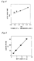
- the n-type semiconductor layer (3) By forming the n-type semiconductor layer (3) with a relatively thin thickness as above, the area of the junction between the n-type drift region (112) and the p-type well region (105) can be decreased, and thus, the output capacitance can be decreased substantially in proportion to the thickness of the semiconductor layer (3) as shown in the graph of Fig. 4 .
- the thickness of the n-type semiconductor layer is thinner than 0.3 ⁇ m, the distance between the n ++ -type source region (106) and the insulating layer (2) becomes smaller, and because of the built-in potential, there is formed such a depletion layer that spreads from the junction between the n ++ -type source region (106) and the p + -type well region (105) into the interior of the p + -type well region (105).
- the p + -type well region (105) between the n ++ -type source region (106) and the insulating layer (2) is apt to come into a pinch-off condition.
- the thickness of the n-type semiconductor layer (3) should be 0.3 ⁇ m or more.
- the SOI-LDMOSFET may include an n-type semiconductor layer (3) with a thickness of 15 ⁇ m.
- the drift distance (the width of the n-type drift region (112)) from an end of the p + -type well region (105) extending along the surface of the n-type semiconductor layer (3) to an end of the n ++ -type drain region (104) should be selected to about 15 ⁇ m.
- the foregoing effects can be obtained.
- the thickness of the n-type semiconductor layer (3) is substantially in the range of 0.3 to 15 ⁇ m. Therefore, when a decrease in output capacitance is needed while it is allowed for the withstand voltage to be relatively low, the thickness of the n-type semiconductor layer (3) is decreased. On the other hand, when higher withstand voltage is required, the thickness of the n-type semiconductor layer (3) is increased.
- the n-type semiconductor layer (3) by increasing the thickness of the n-type semiconductor layer (3), heat can be efficiently released through the n-type drift region (112), so that the resulting element can have an improved thermal resistance feature. Thus, it becomes possible to increase the allowable current in the state of ON.
- the thickness of the n-type semiconductor layer (3) should be 15 ⁇ m or less.
- the SOI-LDMOSFET of the first embodiment of the present invention it is possible to form the n-type drift region (112) with a thickness of about 15 ⁇ m, and therefore possible to construct the SOI-LDMOSFET in practical time, having very high withstand voltage (to about 300 V) and also a large amount of allowable current in the state of ON.
- the thickness of the n-type drift region (112) should be set at 0.5 ⁇ m or more so as to hold the output capacitance relatively small, and the reason therefor is described below.
- the withstand voltage further lowers when the thickness of the n-type semiconductor layer (3) becomes thinner than about 0.5 ⁇ m.
- a design for decreasing the value of (output capacitance) X (on-state resistance) should be made after a required withstand voltage has been ensured by setting the thickness of the n-type semiconductor layer (3) at about 0.5 ⁇ m or more.
- the thickness of the n-type semiconductor layer (3) is set at 0.5 ⁇ m or more in order to increase the allowable current in the state of ON while ensuring high withstand voltage and also to efficiently decrease the value of (output capacitance) X (on-state resistance).
- the thickness of the n-type semiconductor layer (3) is set at about 4 ⁇ m, and where the length of the n-type drift region (112) (in other words, the drift distance) from an end of the p + -type well region (105) to an end of the n ++ -type drain region (104) is set at about 4 ⁇ m.
- the withstand voltage can achieve the class of 100 V (see Fig. 5 ).
- the thermal resistance is decreased, and therefore, the allowable current in the state of ON can be increased.
- the SOI-LDMOSFET of this embodiment by setting the drift distance at 4 ⁇ m and the thickness of the n-type semiconductor layer (3) at about 4 ⁇ m, it is possible to provide a switching element capable of turning a high frequency signal on or off, ensuring withstand voltage of 100 V class which is acutely demanded for relatively high voltage-resistant switching elements, and increasing the allowable current in the state of ON.
- the thickness of the n-type semiconductor layer (3) should be selected within a range of 0.5 to 4 ⁇ m in accordance with the requirement of end use, in case where the withstand voltage is required to achieve the class of 100 V, and where the output capacitance and the on-state resistance are required to be relatively small.
- the thickness of the n-type semiconductor layer (3) should be selected within a range of 4 to 15 ⁇ m in accordance with the requirement of end use, in case where the withstand voltage is required to achieve the class of 100 to 300 V.
- an element having withstand voltage of 25 to 50 V class which has the largest demand in the switches for turning high frequency signals on or off is constructed according to the first embodiment of the present invention.
- This element is constructed taken into account the variation in the thickness of the n-type semiconductor layer (3) within a range of about 0.5 to about 1.5 ⁇ m which is found when the n-type semiconductor layer (3) is formed on a SOI substrate.
- the length of the n-type drift region (112) (in other words, the drift distance) from an end of the p + -type well region (105) extending along the surface of the n-type semiconductor layer (3) to an end of the n ++ -type drain region (104) is selected within a range of 1 to 2 ⁇ m.
- the drift distance of 1 to 2 ⁇ m makes it possible to achieve withstand voltage of 25 to 50 V class which has the largest demand in the switching elements for turning high frequency signals on or off (see Fig. 5 ).
- the thickness of the n-type semiconductor layer (3) should be set at about 0.5 ⁇ m in order to efficiently decrease the value of (output capacitance) X (on-state resistance) (see Fig. 6 ).
- the thickness of the n-type semiconductor layer (3) formed on a provided SOI wafer has a variation of about 0.5 to about 1.5 ⁇ m because of the limit in controllability of growth of thin layers and so on.
- the SOI-LDMOSFET of this embodiment of the present invention by selecting the drift distance within the range of 1 to 2 ⁇ m, a withstand voltage of 25 to 50 V class can be achieved, and the value of (output capacitance) X (on-state resistance) can be decreased to a relatively small value, and further, the allowable current in the state of ON can be increased to a relatively large value.
- a LDMOSFET (200) according to the second embodiment of the present invention is constructed in the same manner as in the LDMOSFET according to the first embodiment, except that an n-type drift region (212) in which the impurity concentration changes stepwise is formed instead of the n-type drift region (112) of the LDEMOSFET of the first embodiment in which the impurity concentration continuously changes.
- FIG. 8A the same reference numerals are used for the same parts as those shown in Fig. 1A .
- the n-type drift region (212) comprises a low concentration region (212a), a medium concentration region (212b) and a high concentration region (212c), and the impurity concentration becomes higher as the distance from the n ++ -type drain region (104) becomes shorter.
- the low concentration region (212a) locates just under the gate overhanging region (113) of the gate electrode (109) and the high concentration region (212c) locates in contact with the n ++ -type drain region (104).
- the impurity concentration Na of the low concentration region (212a) of the n-type drift region (212) is set at a value lower than N(RESURF), and it is preferable that the impurity concentration Nc of the high concentration region (212c) thereof should be set at a value not less than N(RESURF).
- the impurity concentration Nb of the medium concentration region (212b) may be set at a value equal to the value of the impurity concentration Na of the low concentration region (212a) or that Nc of the high concentration region (212c), and preferably, Nb is set at a value satisfying the condition of Na ⁇ Nb ⁇ Nc.
- the n-type drift region (212) may have an impurity concentration distribution in which each of the low concentration region (212a), the medium concentration region (212b) and the high concentration region (212c) has an impurity concentration distribution in which the concentration of each impurity becomes lower as the distance from the n ++ -type drain region (104) becomes longer.
- the impurity concentration discontinuously changes at the interface between each of the regions adjacent to each other.
- the impurity concentration Na of the low concentration region (212a) which locates just under the gate overhanging region (113) is set at a low value, and therefore, a depletion layer can be effectively spread in the low concentration region (212a) in the state of OFF in which the gate voltage is negative or has zero potential. By doing so, it becomes possible to increase the width of the depletion layer in the n-type drift region (212) in the state of OFF, so that the capacitance between the source region and the drain region can be more decreased.
- the impurity concentration Nc of the high concentration region (212c) is set at a relatively high value, and therefore, the carrier concentration of the high concentration region (212c) naturally becomes higher, so that the on-state resistance can be decreased.
- the n-type drift region (212) of the LDMOSFET of the second embodiment can operate in the same manner as the n-type drift region (112) of the first embodiment, so that the LDMOSFET of the second embodiment can provide the same effects as those provided by the LDMOSFET of the first embodiment.
- an oxide layer is formed on the surface of a SOI substrate, and subjected to patterning to form an oxide layer (1115) (see Fig. 9A ).
- n-type impurity for forming a low concentration region (212a) is injected to the regions for n ++ -type drain region and n-type drift region (see Fig. 9B ). Then, the n-type impurity is diffused to a predetermined length by heating.
- a resist (1117) for covering up to a region for forming the low concentration region (212a) is formed, and a little larger dose of n-type impurity for forming a medium concentration region (212b) is injected (see Fig. 9C ). Then, the n-type impurity is diffused to a predetermined length by heating.
- a resist (1118) for covering up to a region for forming the medium concentration region (212b) is formed, and a large dose of n-type impurity for forming a high concentration region (212c) is injected (see Fig. 9D ). Then, the n-type impurity is treated by heat and diffused to a predetermined length.
- n-type impurities are injected and diffused by heating, separately in three stages, so that an n-type drift region (212) in which the impurity concentration changes stepwise between each of the respective regions is formed.
- an impurity for forming a p + -type well region (105) is injected through the oxide layer mask (1115) and a resist mask (1119) and treated by heat, so that the p + -type well region (105) which reaches up to the insulating layer (2) is formed.
- a resist mask (1120) for forming an n ++ -type source region (106) and an n ++ -type drain region (104) is formed, and an n-type impurity is injected through the resist mask (1120) and the silicon oxide layer (1115) as the mask so as to form n-type impurity-implanted regions (104a) and (106a) (see Fig. 9F ).
- the resist mask (1120) is removed, and then, a resist mask (1121) for forming a p ++ -type base contact region is formed, and a p-type impurity is injected through the resist mask (1121) to form a p-type impurity-implanted region (107a) (see Fig. 9G ).
- the resist mask (1121) is removed, and a heat treatment is carried out to diffuse the respective impurities in the n-type impurity-implanted regions (104a) and (106a) and the p-type impurity-implanted region (107a), so that the n ++ -type drain region (104), the n ++ -type source region (106) and the p ++ -type base contact region (107) are formed, respectively.
- a silicon oxide layer (108) for a gate oxide layer is formed (see Fig. 9H ).
- a gate electrode (109) is formed on the silicon oxide layer (108), and an intermediate layer (1122) is further formed, and a part of the intermediate layer (1122) for forming drain, source and base contact regions is removed by etching (see Fig. 9I ).
- a drain electrode (110) and a source electrode (111) are formed, and finally, a protective layer (1123) is formed to thereby complete the LDMOSFET according to the second embodiment.
- the impurity concentration distribution of the n-type drift region (212) can be formed, spending a relatively short time in diffusing the impurities, in case where the n-type semiconductor layer (3) is thin and the drift length is relatively long.
Landscapes
- Engineering & Computer Science (AREA)
- Microelectronics & Electronic Packaging (AREA)
- Power Engineering (AREA)
- Physics & Mathematics (AREA)
- Ceramic Engineering (AREA)
- Condensed Matter Physics & Semiconductors (AREA)
- General Physics & Mathematics (AREA)
- Computer Hardware Design (AREA)
- Manufacturing & Machinery (AREA)
- Thin Film Transistor (AREA)
- Junction Field-Effect Transistors (AREA)
- Insulated Gate Type Field-Effect Transistor (AREA)
Claims (8)
- Dispositif semiconducteur comprenant une couche semiconductrice (3) formée sur un substrat semiconducteur (1), ladite couche semiconductrice comprenant:une région de drain de premier type de conductivité (104) formée dans une partie de la couche semiconductrice, une région de puits de deuxième type de conductivité (105) formée dans une partie de la couche semiconductrice et écartée de la région de drain (104),une région de source de premier type de conductivité (106) formée dans la région de puits (105) et écartée d'une extrémité de la région de puits (105) sur le côté de la région de drain (104),une région de dérive de premier type de conductivité (112, 212), formée entre une extrémité de la région de puits (105) et la région de drain (104) et en contact tout à la fois avec la région de puits (105) et la région de drain (104), la concentration d'impuretés de ladite région de dérive diminuant tout à la fois dans la direction latérale et dans la direction verticale lorsque la distance à partir de la région de drain (104) augmente, la direction latérale étant parallèle à une surface supérieure de la couche semiconductrice, la direction verticale étant perpendiculaire à ladite surface supérieure de la couche semiconductrice,une couche d'oxyde de grille (108) formée sur la région de puits (105) située entre la région de dérive et la région de source (106), etune électrode de grille (109) formée sur la couche d'oxyde de grille (108),dans lequel l'électrode de grille (109) est formée de façon à surplomber la région de dérive (112, 212) pour couvrir une première partie de la région de dérive,caractérisé en ce que la concentration d'impuretés de ladite première partie de la région de dérive est inférieure à la concentration d'impuretés qui satisfait à la condition RESURF.
- Dispositif semiconducteur selon la revendication 1, dans lequel la couche semiconductrice (3) est formée sur une couche isolante (2) sur le substrat semiconducteur (1) .
- Dispositif semiconducteur selon la revendication 1 ou la revendication 2, dans lequel la concentration d'impuretés dans la direction latérale de la région de dérive (112, 212) change en obéissant à la distribution gaussienne ayant, comme paramètre, la distance (x) à partir de la région de drain dans la direction latérale, et la concentration d'impuretés dans la direction verticale de la région de dérive change en obéissant à la distribution gaussienne ayant, comme paramètre, la distance (y) à partir de la région de drain (104) dans la direction verticale.
- Dispositif semiconducteur selon l'une quelconque des revendications 1 à 3, dans lequel la concentration d'impuretés d'une deuxième partie de la région de dérive (112, 212) au voisinage de la région de drain (104) est supérieure à la concentration d'impuretés qui satisfait à la condition RESURF.
- Dispositif semiconducteur selon l'une quelconque des revendications 1 à 4, dans lequel l'épaisseur (t) de la couche semiconductrice est établie à l'intérieur d'une plage de 0,3 µm ≤ t ≤ 15 µm.
- Dispositif semiconducteur selon l'une quelconque des revendications 1 à 5, dans lequel l'épaisseur (t) de la couche semiconductrice est établie à l'intérieur d'une plage de 0,5 µm ≤ t ≤ 4 µm.
- Dispositif semiconducteur selon l'une quelconque des revendications 1 à 6, dans lequel l'épaisseur (t) de la couche semiconductrice est établie à l'intérieur d'une plage de 0,5 µm ≤ t ≤ 1,5 µm.
- Dispositif semiconducteur selon l'une quelconque des revendications 1 à 7, dans lequel la distance de la région de dérive (112, 212) d'une extrémité de la région de drain (104) à une extrémité de la région de puits (105) est établie à 15 µm ou moins.
Applications Claiming Priority (2)
| Application Number | Priority Date | Filing Date | Title |
|---|---|---|---|
| JP36491999 | 1999-12-22 | ||
| JP36491999 | 1999-12-22 |
Publications (3)
| Publication Number | Publication Date |
|---|---|
| EP1111687A2 EP1111687A2 (fr) | 2001-06-27 |
| EP1111687A3 EP1111687A3 (fr) | 2005-07-06 |
| EP1111687B1 true EP1111687B1 (fr) | 2011-06-22 |
Family
ID=18482988
Family Applications (1)
| Application Number | Title | Priority Date | Filing Date |
|---|---|---|---|
| EP00128104A Expired - Lifetime EP1111687B1 (fr) | 1999-12-22 | 2000-12-21 | Dispositif semi-conducteur MOS |
Country Status (7)
| Country | Link |
|---|---|
| US (1) | US6448620B2 (fr) |
| EP (1) | EP1111687B1 (fr) |
| JP (1) | JP4106869B2 (fr) |
| KR (1) | KR100412338B1 (fr) |
| CN (1) | CN1220270C (fr) |
| SG (1) | SG105478A1 (fr) |
| TW (1) | TW564557B (fr) |
Cited By (2)
| Publication number | Priority date | Publication date | Assignee | Title |
|---|---|---|---|---|
| US8552496B2 (en) | 2001-09-07 | 2013-10-08 | Power Integrations, Inc. | High-voltage vertical transistor with edge termination structure |
| US8940605B2 (en) | 2001-09-07 | 2015-01-27 | Power Integrations, Inc. | Method of fabricating a high-voltage transistor with an extended drain structure |
Families Citing this family (27)
| Publication number | Priority date | Publication date | Assignee | Title |
|---|---|---|---|---|
| US7221011B2 (en) * | 2001-09-07 | 2007-05-22 | Power Integrations, Inc. | High-voltage vertical transistor with a multi-gradient drain doping profile |
| US20030107050A1 (en) * | 2001-12-10 | 2003-06-12 | Koninklijke Philips Electronics N.V. | High frequency high voltage silicon-on-insulator device with mask variable inversion channel and method for forming the same |
| JP3634830B2 (ja) | 2002-09-25 | 2005-03-30 | 株式会社東芝 | 電力用半導体素子 |
| CN100388442C (zh) * | 2003-05-23 | 2008-05-14 | 上海宏力半导体制造有限公司 | 可改善组件特性的高压组件的制造方法 |
| GB0418573D0 (en) * | 2004-08-20 | 2004-09-22 | Koninkl Philips Electronics Nv | Semiconductor devices and the manufacture thereof |
| JP2006202948A (ja) * | 2005-01-20 | 2006-08-03 | Toshiba Corp | 半導体素子 |
| JP4857590B2 (ja) * | 2005-04-19 | 2012-01-18 | サンケン電気株式会社 | 半導体素子 |
| KR101201496B1 (ko) * | 2005-12-23 | 2012-11-14 | 매그나칩 반도체 유한회사 | 수평 확산형 모스 트랜지스터 및 그 제조방법 |
| JP5479671B2 (ja) * | 2007-09-10 | 2014-04-23 | ローム株式会社 | 半導体装置 |
| USRE45449E1 (en) | 2007-12-27 | 2015-04-07 | Infineon Technologies Ag | Power semiconductor having a lightly doped drift and buffer layer |
| CN101751595B (zh) * | 2008-12-04 | 2011-12-07 | 北京中电华大电子设计有限责任公司 | 一种提高io速度的电路 |
| KR101128694B1 (ko) * | 2009-11-17 | 2012-03-23 | 매그나칩 반도체 유한회사 | 반도체 장치 |
| JP5554415B2 (ja) * | 2010-10-15 | 2014-07-23 | 三菱電機株式会社 | 半導体装置およびその製造方法 |
| US8860132B2 (en) * | 2011-11-30 | 2014-10-14 | Infineon Technologies Austria Ag | Semiconductor device arrangement comprising a semiconductor device with a drift region and a drift control region |
| TWI467766B (zh) * | 2012-08-31 | 2015-01-01 | Nuvoton Technology Corp | 金氧半場效電晶體及其製造方法 |
| US9202910B2 (en) * | 2013-04-30 | 2015-12-01 | Infineon Technologies Austria Ag | Lateral power semiconductor device and method for manufacturing a lateral power semiconductor device |
| JP6327747B2 (ja) * | 2014-04-23 | 2018-05-23 | 株式会社 日立パワーデバイス | 半導体装置 |
| KR102286014B1 (ko) | 2015-11-23 | 2021-08-06 | 에스케이하이닉스 시스템아이씨 주식회사 | 개선된 온저항 및 브레이크다운전압을 갖는 고전압 집적소자 |
| CN107808902B (zh) * | 2017-09-11 | 2021-06-18 | 西安电子科技大学 | 一种具有多环电场调制衬底的宽带隙半导体横向双扩散晶体管 |
| CN107768424B (zh) * | 2017-09-11 | 2021-06-18 | 西安电子科技大学 | 一种具有多环电场调制衬底的宽带隙半导体横向超结双扩散晶体管 |
| CN107681004B (zh) * | 2017-09-11 | 2021-08-20 | 西安电子科技大学 | 一种具有多环电场调制衬底的元素半导体横向双扩散晶体管 |
| CN110690267B (zh) * | 2018-07-06 | 2023-03-24 | 立锜科技股份有限公司 | 高压元件及其制造方法 |
| CN111524965B (zh) * | 2020-04-29 | 2021-09-24 | 电子科技大学 | 降低高压互连影响的横向器件及制备方法 |
| CN111524962B (zh) * | 2020-04-29 | 2022-02-08 | 电子科技大学 | 降低高压互连影响的器件结构及制造方法 |
| CN111524964B (zh) * | 2020-04-29 | 2021-09-24 | 电子科技大学 | 降低高压互连影响的横向器件及制备方法 |
| CN111524963B (zh) * | 2020-04-29 | 2021-09-24 | 电子科技大学 | 降低高压互连影响的器件结构及制造方法 |
| CN111524966B (zh) * | 2020-04-29 | 2021-08-03 | 电子科技大学 | 一种降低高压互连影响的横向高压器件 |
Family Cites Families (11)
| Publication number | Priority date | Publication date | Assignee | Title |
|---|---|---|---|---|
| US5246870A (en) | 1991-02-01 | 1993-09-21 | North American Philips Corporation | Method for making an improved high voltage thin film transistor having a linear doping profile |
| EP0497427B1 (fr) * | 1991-02-01 | 1996-04-10 | Koninklijke Philips Electronics N.V. | Dispositif semi-conducteur pour des applications à haute-tension et sa méthode de fabrication |
| US5371394A (en) * | 1993-11-15 | 1994-12-06 | Motorola, Inc. | Double implanted laterally diffused MOS device and method thereof |
| JPH08181321A (ja) * | 1994-12-26 | 1996-07-12 | Matsushita Electric Works Ltd | Soi基板及びその製造方法 |
| TW360982B (en) * | 1996-01-26 | 1999-06-11 | Matsushita Electric Works Ltd | Thin film transistor of silicon-on-insulator type |
| SE513283C2 (sv) * | 1996-07-26 | 2000-08-14 | Ericsson Telefon Ab L M | MOS-transistorstruktur med utsträckt driftregion |
| KR100225411B1 (ko) * | 1997-03-24 | 1999-10-15 | 김덕중 | LDMOS(a lateral double-diffused MOS) 트랜지스터 소자 및 그의 제조 방법 |
| KR100244282B1 (ko) * | 1997-08-25 | 2000-02-01 | 김영환 | 고전압 트랜지스터의 구조 및 제조 방법 |
| JP3315356B2 (ja) * | 1997-10-15 | 2002-08-19 | 株式会社東芝 | 高耐圧半導体装置 |
| JPH11204786A (ja) * | 1998-01-14 | 1999-07-30 | Mitsubishi Electric Corp | 高耐圧絶縁ゲート型電界効果トランジスタを有する半導体装置およびその製造方法 |
| JP2000332247A (ja) * | 1999-03-15 | 2000-11-30 | Toshiba Corp | 半導体装置 |
-
2000
- 2000-12-21 TW TW089127571A patent/TW564557B/zh not_active IP Right Cessation
- 2000-12-21 EP EP00128104A patent/EP1111687B1/fr not_active Expired - Lifetime
- 2000-12-22 KR KR10-2000-0080284A patent/KR100412338B1/ko active IP Right Grant
- 2000-12-22 CN CNB001374532A patent/CN1220270C/zh not_active Expired - Lifetime
- 2000-12-22 US US09/741,812 patent/US6448620B2/en not_active Expired - Lifetime
- 2000-12-22 JP JP2000391436A patent/JP4106869B2/ja not_active Expired - Lifetime
- 2000-12-22 SG SG200007620A patent/SG105478A1/en unknown
Cited By (2)
| Publication number | Priority date | Publication date | Assignee | Title |
|---|---|---|---|---|
| US8552496B2 (en) | 2001-09-07 | 2013-10-08 | Power Integrations, Inc. | High-voltage vertical transistor with edge termination structure |
| US8940605B2 (en) | 2001-09-07 | 2015-01-27 | Power Integrations, Inc. | Method of fabricating a high-voltage transistor with an extended drain structure |
Also Published As
| Publication number | Publication date |
|---|---|
| EP1111687A2 (fr) | 2001-06-27 |
| KR100412338B1 (ko) | 2003-12-31 |
| JP4106869B2 (ja) | 2008-06-25 |
| EP1111687A3 (fr) | 2005-07-06 |
| US6448620B2 (en) | 2002-09-10 |
| CN1301044A (zh) | 2001-06-27 |
| US20010013624A1 (en) | 2001-08-16 |
| CN1220270C (zh) | 2005-09-21 |
| JP2001244472A (ja) | 2001-09-07 |
| KR20010062630A (ko) | 2001-07-07 |
| TW564557B (en) | 2003-12-01 |
| SG105478A1 (en) | 2004-08-27 |
Similar Documents
| Publication | Publication Date | Title |
|---|---|---|
| EP1111687B1 (fr) | Dispositif semi-conducteur MOS | |
| US10084037B2 (en) | MOSFET active area and edge termination area charge balance | |
| US9129822B2 (en) | High voltage field balance metal oxide field effect transistor (FBM) | |
| KR100829052B1 (ko) | 전력 mosfet, 이를 형성하는 방법, 및 이 방법에의해 형성되는 다른 전력 mosfet | |
| EP0735591B1 (fr) | Structure d'un dispositif DMOS et sa méthode de fabrication | |
| EP0616372B1 (fr) | Transistor DMOS à canal court avec tranchée | |
| US5342797A (en) | Method for forming a vertical power MOSFET having doped oxide side wall spacers | |
| US7091552B2 (en) | High voltage power MOSFET having a voltage sustaining region that includes doped columns formed by trench etching and ion implantation | |
| EP0696054A1 (fr) | Procédé de manufacture des dispositifs de puissance à haute densité en technology MOS | |
| KR20010023861A (ko) | 반도체 전력 장치의 제조 방법 | |
| WO2005081323A2 (fr) | Dispositifs a semi-conducteur a tranchees-grilles et fabrication | |
| CN101889327A (zh) | 具有带易于浮岛形成的台阶式沟槽的电压维持层的功率半导体器件的制造方法 | |
| EP0693773B1 (fr) | Dispositif de puissance du type VDMOS et sol procédé de fabrication | |
| US6784488B2 (en) | Trench-gate semiconductor devices and the manufacture thereof | |
| US6054737A (en) | High density MOS technology power device | |
| EP0613186A1 (fr) | Transistor lateral complètement épuisé | |
| KR20000029577A (ko) | 선형전류-전압특성을가지는반도체부품 | |
| EP1104027B1 (fr) | Dispositif semi-conducteur de puissance comprenant une région à résistance ballast | |
| WO2004042825A1 (fr) | Dispositifs a semi-conducteur et leurs procedes de fabrication | |
| EP0817274B1 (fr) | Dispositif de puissance en technologie MOS asymétrique | |
| EP0776048B1 (fr) | Procédé de fabrication d'un dispositif MOS ayant une région de base à haute résistance de claquage | |
| US20090020832A1 (en) | Semiconductor Devices and the Manufacture Thereof | |
| KR20040065224A (ko) | 트렌치 게이트 반도체 디바이스 및 이의 제조 방법 | |
| Vaid et al. | Investigation of a power FLIMOSFET based on two-dimensional numerical simulations | |
| WO2009004583A1 (fr) | Transistor à effet de champ à grille en tranchée et son procédé de fabrication |
Legal Events
| Date | Code | Title | Description |
|---|---|---|---|
| PUAI | Public reference made under article 153(3) epc to a published international application that has entered the european phase |
Free format text: ORIGINAL CODE: 0009012 |
|
| 17P | Request for examination filed |
Effective date: 20010119 |
|
| AK | Designated contracting states |
Kind code of ref document: A2 Designated state(s): AT BE CH CY DE DK ES FI FR GB GR IE IT LI LU MC NL PT SE TR |
|
| AX | Request for extension of the european patent |
Free format text: AL;LT;LV;MK;RO;SI |
|
| PUAL | Search report despatched |
Free format text: ORIGINAL CODE: 0009013 |
|
| AK | Designated contracting states |
Kind code of ref document: A3 Designated state(s): AT BE CH CY DE DK ES FI FR GB GR IE IT LI LU MC NL PT SE TR |
|
| AX | Request for extension of the european patent |
Extension state: AL LT LV MK RO SI |
|
| RIC1 | Information provided on ipc code assigned before grant |
Ipc: 7H 01L 29/786 B Ipc: 7H 01L 29/08 B Ipc: 7H 01L 29/36 B Ipc: 7H 01L 29/78 A Ipc: 7H 01L 21/336 B |
|
| AKX | Designation fees paid |
Designated state(s): DE FR GB IT NL SE |
|
| RAP1 | Party data changed (applicant data changed or rights of an application transferred) |
Owner name: PANASONIC ELECTRIC WORKS CO., LTD. |
|
| 17Q | First examination report despatched |
Effective date: 20090313 |
|
| RIC1 | Information provided on ipc code assigned before grant |
Ipc: H01L 29/786 20060101ALI20101029BHEP Ipc: H01L 29/36 20060101ALI20101029BHEP Ipc: H01L 29/78 20060101AFI20101029BHEP Ipc: H01L 21/336 20060101ALN20101029BHEP Ipc: H01L 29/08 20060101ALI20101029BHEP |
|
| RTI1 | Title (correction) |
Free format text: MOS SEMICONDUCTOR DEVICE |
|
| GRAP | Despatch of communication of intention to grant a patent |
Free format text: ORIGINAL CODE: EPIDOSNIGR1 |
|
| GRAS | Grant fee paid |
Free format text: ORIGINAL CODE: EPIDOSNIGR3 |
|
| GRAA | (expected) grant |
Free format text: ORIGINAL CODE: 0009210 |
|
| RIN1 | Information on inventor provided before grant (corrected) |
Inventor name: SUZUKI, YUJI Inventor name: SUZUMURA, MASAHIKO Inventor name: TAKANO, HITOMICHI Inventor name: HAYASAKI, YOSHIKI Inventor name: SHIRAI, YOSHIFUMI Inventor name: YOSHIHARA, TAKAAKI Inventor name: YOSHIDA, TAKESHI Inventor name: KISHIDA, TAKASHI |
|
| AK | Designated contracting states |
Kind code of ref document: B1 Designated state(s): DE FR GB IT NL SE |
|
| REG | Reference to a national code |
Ref country code: GB Ref legal event code: FG4D |
|
| REG | Reference to a national code |
Ref country code: DE Ref legal event code: R096 Ref document number: 60046098 Country of ref document: DE Effective date: 20110728 |
|
| REG | Reference to a national code |
Ref country code: NL Ref legal event code: VDEP Effective date: 20110622 |
|
| PG25 | Lapsed in a contracting state [announced via postgrant information from national office to epo] |
Ref country code: SE Free format text: LAPSE BECAUSE OF FAILURE TO SUBMIT A TRANSLATION OF THE DESCRIPTION OR TO PAY THE FEE WITHIN THE PRESCRIBED TIME-LIMIT Effective date: 20110622 |
|
| PG25 | Lapsed in a contracting state [announced via postgrant information from national office to epo] |
Ref country code: NL Free format text: LAPSE BECAUSE OF FAILURE TO SUBMIT A TRANSLATION OF THE DESCRIPTION OR TO PAY THE FEE WITHIN THE PRESCRIBED TIME-LIMIT Effective date: 20110622 |
|
| PLBE | No opposition filed within time limit |
Free format text: ORIGINAL CODE: 0009261 |
|
| STAA | Information on the status of an ep patent application or granted ep patent |
Free format text: STATUS: NO OPPOSITION FILED WITHIN TIME LIMIT |
|
| 26N | No opposition filed |
Effective date: 20120323 |
|
| REG | Reference to a national code |
Ref country code: DE Ref legal event code: R097 Ref document number: 60046098 Country of ref document: DE Effective date: 20120323 |
|
| REG | Reference to a national code |
Ref country code: FR Ref legal event code: PLFP Year of fee payment: 16 |
|
| PGFP | Annual fee paid to national office [announced via postgrant information from national office to epo] |
Ref country code: GB Payment date: 20151221 Year of fee payment: 16 |
|
| PGFP | Annual fee paid to national office [announced via postgrant information from national office to epo] |
Ref country code: FR Payment date: 20151221 Year of fee payment: 16 |
|
| PGFP | Annual fee paid to national office [announced via postgrant information from national office to epo] |
Ref country code: IT Payment date: 20151221 Year of fee payment: 16 |
|
| GBPC | Gb: european patent ceased through non-payment of renewal fee |
Effective date: 20161221 |
|
| REG | Reference to a national code |
Ref country code: FR Ref legal event code: ST Effective date: 20170831 |
|
| PG25 | Lapsed in a contracting state [announced via postgrant information from national office to epo] |
Ref country code: FR Free format text: LAPSE BECAUSE OF NON-PAYMENT OF DUE FEES Effective date: 20170102 Ref country code: IT Free format text: LAPSE BECAUSE OF NON-PAYMENT OF DUE FEES Effective date: 20161221 |
|
| PG25 | Lapsed in a contracting state [announced via postgrant information from national office to epo] |
Ref country code: GB Free format text: LAPSE BECAUSE OF NON-PAYMENT OF DUE FEES Effective date: 20161221 |
|
| PGFP | Annual fee paid to national office [announced via postgrant information from national office to epo] |
Ref country code: DE Payment date: 20191210 Year of fee payment: 20 |
|
| REG | Reference to a national code |
Ref country code: DE Ref legal event code: R071 Ref document number: 60046098 Country of ref document: DE |