EP1109029A1 - Appareil pour tester des conducteurs électriques utilisant l'effet photoélectrique - Google Patents
Appareil pour tester des conducteurs électriques utilisant l'effet photoélectrique Download PDFInfo
- Publication number
- EP1109029A1 EP1109029A1 EP00108285A EP00108285A EP1109029A1 EP 1109029 A1 EP1109029 A1 EP 1109029A1 EP 00108285 A EP00108285 A EP 00108285A EP 00108285 A EP00108285 A EP 00108285A EP 1109029 A1 EP1109029 A1 EP 1109029A1
- Authority
- EP
- European Patent Office
- Prior art keywords
- trace
- electrode
- traces
- photoelectric effect
- board
- Prior art date
- Legal status (The legal status is an assumption and is not a legal conclusion. Google has not performed a legal analysis and makes no representation as to the accuracy of the status listed.)
- Withdrawn
Links
Images


Classifications
-
- H—ELECTRICITY
- H05—ELECTRIC TECHNIQUES NOT OTHERWISE PROVIDED FOR
- H05K—PRINTED CIRCUITS; CASINGS OR CONSTRUCTIONAL DETAILS OF ELECTRIC APPARATUS; MANUFACTURE OF ASSEMBLAGES OF ELECTRICAL COMPONENTS
- H05K13/00—Apparatus or processes specially adapted for manufacturing or adjusting assemblages of electric components
- H05K13/08—Monitoring manufacture of assemblages
-
- G—PHYSICS
- G01—MEASURING; TESTING
- G01R—MEASURING ELECTRIC VARIABLES; MEASURING MAGNETIC VARIABLES
- G01R31/00—Arrangements for testing electric properties; Arrangements for locating electric faults; Arrangements for electrical testing characterised by what is being tested not provided for elsewhere
- G01R31/28—Testing of electronic circuits, e.g. by signal tracer
- G01R31/302—Contactless testing
- G01R31/308—Contactless testing using non-ionising electromagnetic radiation, e.g. optical radiation
- G01R31/309—Contactless testing using non-ionising electromagnetic radiation, e.g. optical radiation of printed or hybrid circuits or circuit substrates
Definitions
- the packaging density has increased considerably, resulting in extremely narrow and thin traces disposed on both sides of the substrates with numerous connections from one side to the other. Fabrication of such fine traces is difficult such that defects are more common. Therefore, testing the quality of fine traces on both sides and connections from one side to the other of a substrate has become increasingly more important.
- This invention is a tester for electrical traces such as on a circuit board, and the preferred embodiment generally comprises a laser producing an ultraviolet beam, a vacuum chamber, an electrode circuit including electrodes and corresponding electronics including ammeters for measuring photoelectron flow between traces and electrodes, a controller, laser beam optics, an image acquisition system, and a pair of broadband UV lights.
- the board containing traces under test is disposed in the vacuum chamber at lowered pressure with grid electrode lying over the trace area on each side of the board. Electrode electronics selectively maintain a known potential on each electrode. The exact location of traces are determined by an image acquisition system.
- the traces are initialized to a known voltage such as by: (1) the induced high voltage method by first applying a relatively high positive voltage to one electrode and a high negative voltage to the other electrode, then reversing the polarity of the voltages; (2) simultaneous photoelectron effect illumination of electrodes by setting both electrodes to a known positive voltage and irradiating electrodes, board and traces by the broadband UV electromagnetic sources; or (3) laser method by setting electrodes to a known voltage and dithering the laser beam so as to strike a portion of electrode and a trace. Shining the laser beam on a location so as to liberate photoelectrons is referred to as "interrogating".
- Continuity between two points on a trace is determined by interrogating the first location until it is charged to a known voltage and then by interrogating the second location.
- Shorts between traces can be determined by interrogating a first trace until it is charged to a known voltage and then interrogating the second trace.
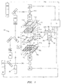
- Figure 1 is a schematic representation of a preferred embodiment of the trace tester of the invention.
- Figure 2 is an enlarged view of the vacuum chamber and its contents of Figure 1.
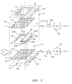
- Figure 3 is an enlarged representation of the image acquisition elements of Figure 1.
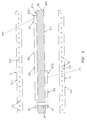
- Figure 5 is an enlarged vertical cross-sectional representation of a representative substrate and nearby elements.
- a substrate 80 such as printed circuit board 80P having an upper side 81U and a lower side 81L, contains electrical traces 85 to be tested.
- a given trace 85 may include upper portions 85U on board upper side 81U and lower portions 85L on board lower side 81L.
- Each trace 85 includes pads 87 for attachment of electrical components and, typically, at the end of each trace 85 is an end pad 87E, such as upper end pad 87EU and lower end pad 87EL.
- a trace 85 passes from upper side 81U to lower side 81L through plated through holes 89.
- Tester 10 tests traces 85 on both upper and lower sides 81U, 81L ofboard80P. Obvious modifications can be made to tester 10 to test traces 85 on only one side of board 80P.
- Trace tester 10 generally comprises an electromagnetic source means 20, vacuum chamber means 12, an electrode circuit 49 including electrodes 51 and corresponding electronics 55, controller 71 and a plurality of broadband electromagnetic source means 18, such as pair 18U, 18L.
- vacuum chamber means may be of conventional, well-known design for creating and controlling the vacuum pressure in a test volume 13 at a specified value.
- Vacuum chamber means 12 includes: a chamber 12C enclosing a test volume 13; an evacuation means, such as vacuum pump 14 for lowering the pressure in test volume 13; doors, not shown, for access; and windows 15, such as upper window 15U and lower window 15L.
- the use of vacuum chamber 12 aids in the efficiency of tester 10.
- Vacuum pump 14 evacuates volume 13 to a rough vacuum.
- FIG 3 is an enlarged representation of the image acquisition elements of Figure 1 by which tester 10 determines the location of test trace 85T in chamber 12C relative to the optical path components.
- the initial accuracy of either manual or machine placement of board 80P within chamber 12 is approximately +/- 1.02 mm (+/- 0.040 inch).
- the precise location of placement of board 80P is determined through the use of image acquisition.
- Controller 71 includes a computer and contains a mapping of traces 85 and other indicia on board 80P. Controller 71 via path 72U directs upper servo mechanism 35U which in turn will rotate upper galvo beam mirror 44U to a predetermined position that will capture the image of a fiducial, a recognizable feature, on upper side 81U of board 80P.
- This image will be reflected through scan lens 46U, upper galvo beam mirror 44U, through upper high reflector 41U, and through upper telescope vision system 47U to upper CCD acquisition system 48U which is connected by line 73U to controller 71.
- the actual position of the fiducial will be compared to the position data supplied by controller 71. This process will be repeated for a second and perhaps a third known fiducial.
- the resulting data will provide an X,Y offset and/or scaling factor that will be applied to position data for each of the upper end pads 87EU of test traces 85T on board 80P.
- controller 71 via line 73L will direct lower servo mechanism 35L, which in turn will rotate lower galvo beam mirror 44L to a predetermined position that will capture the image of a fiducial on the lower side 81L of board 80P.
- This image will be reflected through scan lens 46L, lower beam galvo beam mirror 44L, through first lower high reflector 41LS, and through the lower telescope vision system 47L to the lower CCD acquisition system 48L which is connected by line 73L to controller 71.
- the actual position of the fiducial will be compared to the position data supplied by controller 71. This process will be repeated for a second and perhaps a third known fiducial.
- the resulting data will provide an X,Y offset and/or a scaling factor that will be applied to position data for each of the lower end pads 87EL of test traces 85T on board 80P.
- controller 70 knows the physical position of traces, 85 on board 80P relative to optical path components.
- Electromagnetic source means 20 generally comprises a source of electromagnetic radiation 21, such as ultraviolet laser 22, for producing a beam 24 of electromagnetic radiation such as of ultraviolet light, and optical path components 38, including a beam splitter 42 for splitting beam 24 into upper and lower beams 24U, 24L, for directing beams 24U, 24L onto chamber 12C.
- a single source 21 is shown for producing beams 24U, 24L, multiple sources could be used.
- Laser 22 may be continuous wave, pulsed, q-switched or mode-locked. Q-switched is preferred.
- Upper beam 24U passes through upper shutter 43U and upper beam conditioning optics 37U, off upper high reflector 41U, to upper galvo beam mirror 44U, then through upper scan lens 46U, window 15U, and the upper electrode 51U, to a specific target, such as on test trace 85T or such as an end pad 87E.
- Scan lenses 46U and 46L have been designed for a flat focused field while maintaining both the visual and the UV wave lengths in the same scan area.
- Shutters 43U and 43L are used to control the time of testing by allowing beams 24U and 24L to illuminate the end pads 87EU and 87EL of trace 85T for specific time periods.
- the shutters 43U and 43L may be electromechanical, piezo electrical, acousto-optic or electro-optic.
- Lower beam 24L reflects off first lower high reflector 41LF, passes through lower shutter 43L and lower beam conditioning optics 37L, off second lower high reflector 41LS, to lower galvo beam mirror 44L, then through lower scan lens 46L and window 15L.
- Galvo beam mirrors 44U, 44L are directed by upper and lower servo mechanisms 35U, 35L to deflect beams 24U, 24L to the desired target.
- Servo mechanisms 35U, 35L are connected to controller 71 by connectors 72U, 72L.
- Controller 71 has a mapping of all traces 85 on board 80P and is programmed to sequentially control and move beams 24U, 24L at selected times to desired test targets.
- beams 24U, 24L entering windows 15U, 15L are of small cross-section, such as focused to approximately 0.076 mm (0.003 inch) or less in diameter over the entire area of board 80P, and are capable of producing the photoelectric effect on targets, thereby liberating electrons, sometimes referred to as photoelectrons, therefrom.
- Electrode circuit 49 includes electrodes 51, such as upper electrode 51U and lower electrode 51L, and is associated electronics 55U, 55L.
- electrodes 51U, 51L are grids 52U, 52L of 0.025 mm (0.001 inch) or smaller wire 53 interlaced on a 0.38 mm (0.015 inch) or tighter pitch.
- Grids 52U, 52L are situated above and below board 80P at distance of approximately 5 mm and lie overand under traces 85. Testing can be accomplished with both larger and shorter separation distances.
- Electrodes 51 include etched plates or film sheets.
- a plate electrode comprises a transparent plate, such as of glass, having a conductive grid pattern, such as of chromium, deposited and etched on the side facing board 80P.
- a film sheet electrode comprises a thin, transparent conductive film sheet, having the surface that is facing board 80P coated (e.g. sputtered) with a controlled amount of conductive metal in the form of a thin conductive, such as metallic, coating that is sufficiently transparent to the beam.
- Electrode electronics 55U, 55L provide voltages to electrodes 51U, 51L on lines 56U, 56L respectively as 20 well as analyze currents through electrodes 51, such as with meters 59, such as ammeters 59U, 59L. Results amassed from the grid electronics are forwarded to the controller 71 on lines 57U, 57L respectively for display and/or recording.
- one electrode 51 such as upper electrode 51U acts as a collector, i.e. a collector of electrons, if the near trace 85 is of lower potential
- one electrode 51 such as lower electrode 51L acts as an emitter, i.e. an emitter of electrons, if the near trace 85 is of higher potential.
- board 80P and traces 85 are initially at an unknown voltage.
- the initial board and trace voltages may be due to static electricity build-up during handling, movement, or vacuum pump-down.
- board 80P and traces 85 with a known voltage initial condition so that reliable, predictable and repeatable tests can be performed. It has been found that well-known means in the art do not work reliably.
- the common practice of passing the board 80P through grounding rollers to give board 80P and traces 85 a zero or neutral voltage does not work reliably because subsequent operations, performed on board 80P before test, such as movement into chamber 12C and vacuum pump-down, may induce static electricity to be formed on board 80P and/or traces 85. Therefore the following methods are used to place all traces 85 at a known initial voltage.
- One method of voltage initialization of board 80P and traces 85 is by induced high voltage.
- all traces 85 are given a known voltage by applying a relatively high positive voltage in the range of 500 to 2,000 volts to one electrode 51 making it a collector 51C while at the same time applying high negative voltage in the range 500 to 2,000 volts to the other electrode 51 making it an emitter 51E such that the resulting high potential field in the presence of natural background electrons initiate an electron flow to be emitted from the emitter electrode 51E and travel towards the more positive collector electrode 51C. Since board 80P is interposed in the space between electrodes 51, many of the electrons strike board 80P, and many electrons are then emitted by board 80P to travel towards collector 51C.
- Another method to give known voltage to traces 85 is to use the laser method where the ultraviolet laser 22 and optical path components 39 are used to simultaneously illuminate a spot on electrode 51 and an individual trace 85T with beam 24U or 24L, after setting electrode 51 to a known voltage in the range of 10 to 100 volts, such that photoelectrons are liberated from electrode 51 and trace 85T and flow until trace 85T is at the same potential as electrode 51.
- beam 24L, 24U may be dithered using controller 71 and galvo beam mirror 44U or 44L to insure that beam 24U, 24L strikes a portion of electrode 51 while the center of motion is aimed at target test pad 87EU or 87EL.
- each trace 85 charges only one trace 85 at a time, so the process described must be repeated for each trace 85. Additionally, each end 87E of each trace 85 must be illuminated by beam 24U or 24L to ensure that a uniform voltage is applied to traces 85 which may have an open circuit.
- Electrode electronics 55U maintain both electrodes 51 as collectors 51C at a given potential for collecting electrons liberated by the photoelectric effect of beams 24U, 24L on trace 85.
- a first location on trace 85 such as on upper end pad 87EU, is interrogated by beam 24U. This charges the first location to a voltage level equal to that of the upper collector 51C.
- beam 24U or 24L is then directed, to another location, such as opposite end pad 87EL of trace 85.
- the second end point is charged, to the same voltage level such that no current is detected, then it may be assumed that continuity exists between the first and second locations. Conversely, if a current is detected then the second location does not exhibit a charge level equal to that of collector 51C and it may be assumed that an open circuit has been detected and the system will display and/or record this as a defect. Each trace 85 is tested for continuity in this manner.
- Test for shorts The test for shorts is performed in a manner similar to that described above of determining continuity or opens. Immediately after determining the validity of a trace for continuity, i.e. no opens, locations, such as end pads 87E of adjacent traces may be interrogated to determine their voltage levels. If the adjacent trace does not exhibit a voltage level equal to that of the collector then it may be assumed that the adjacent trace is isolated from the initial trace. If an adjacent trace exhibits a voltage level equal to that of the initial trace, such as by meter 59 showing no current flow, then it may be assumed that a short exists between the two traces allowing the second trace to charge to collector voltage level simultaneously with the initial trace. Tester 10 will display and/or record this as a defect.
- All adjacent traces must be tested in a like manner to assure that the initial trace tested is not shorted to any other trace on board 80P.
- a further advantage of the invention is the ability to quickly retest individual traces 85T which may have failed initial testing.
- the method is as described earlier except that initial charging to a known voltage is performed with the laser method using the beam 24U or 24L since not all traces must be recharged, only those that failed initial testing.
Landscapes
- Engineering & Computer Science (AREA)
- Physics & Mathematics (AREA)
- General Engineering & Computer Science (AREA)
- Computer Vision & Pattern Recognition (AREA)
- Electromagnetism (AREA)
- Toxicology (AREA)
- Health & Medical Sciences (AREA)
- General Physics & Mathematics (AREA)
- Operations Research (AREA)
- Manufacturing & Machinery (AREA)
- Microelectronics & Electronic Packaging (AREA)
- Tests Of Electronic Circuits (AREA)
- Measuring Leads Or Probes (AREA)
- Testing Of Short-Circuits, Discontinuities, Leakage, Or Incorrect Line Connections (AREA)
Applications Claiming Priority (2)
| Application Number | Priority Date | Filing Date | Title |
|---|---|---|---|
| US461801 | 1983-01-28 | ||
| US09/461,801 US6369591B1 (en) | 1999-01-14 | 1999-12-15 | Apparatus and method using photoelectric effect for testing electrical traces |
Publications (1)
| Publication Number | Publication Date |
|---|---|
| EP1109029A1 true EP1109029A1 (fr) | 2001-06-20 |
Family
ID=23833984
Family Applications (1)
| Application Number | Title | Priority Date | Filing Date |
|---|---|---|---|
| EP00108285A Withdrawn EP1109029A1 (fr) | 1999-12-15 | 2000-04-14 | Appareil pour tester des conducteurs électriques utilisant l'effet photoélectrique |
Country Status (5)
| Country | Link |
|---|---|
| US (1) | US6369591B1 (fr) |
| EP (1) | EP1109029A1 (fr) |
| JP (1) | JP2001174499A (fr) |
| KR (1) | KR20010066778A (fr) |
| CN (1) | CN1195988C (fr) |
Cited By (4)
| Publication number | Priority date | Publication date | Assignee | Title |
|---|---|---|---|---|
| EP1233275A2 (fr) * | 2001-02-19 | 2002-08-21 | Nihon Densan Read Kabushiki Kaisha, (Nidec-Read Corporation) | Appareil et procédé pour tester des circuits imprimés |
| US7202690B2 (en) | 2001-02-19 | 2007-04-10 | Nidec-Read Corporation | Substrate inspection device and substrate inspecting method |
| FR2927703A1 (fr) * | 2008-02-14 | 2009-08-21 | Beamind Soc Par Actions Simpli | Procede de test de conducteurs electriques par photoelectricite, a courant de test non nul. |
| FR2927702A1 (fr) * | 2008-02-14 | 2009-08-21 | Beamind Soc Par Actions Simpli | Systeme de test sans contact de circuits electriques par effet photoelectrique. |
Families Citing this family (9)
| Publication number | Priority date | Publication date | Assignee | Title |
|---|---|---|---|---|
| FR2801680B3 (fr) * | 1999-11-26 | 2002-02-15 | Christophe Vaucher | Methode de test electrique de la conformite de l'interconnexion de conducteurs electriques disposes sur un substrat, sans contact et sans outillage |
| DE10038313A1 (de) * | 2000-08-05 | 2002-02-21 | Tsk Pruefsysteme Fuer Elek Sch | Verfahren und Vorrichtung zur Prüfung von Leiterplatten auf Funktionsfähigkeit |
| US6894518B1 (en) * | 2002-03-29 | 2005-05-17 | Advanced Micro Devices, Inc. | Circuit analysis and manufacture using electric field-induced effects |
| FR2881834B1 (fr) * | 2005-02-04 | 2007-05-11 | Beamind Soc Par Actions Simpli | Procede et systeme de test ou de mesure d'elements electriques, au moyen de deux impulsions decalees |
| FR2881835B1 (fr) * | 2005-02-04 | 2007-07-27 | Beamind Soc Par Actions Simpli | Procede et systeme de test ou de mesure d'elements electriques |
| WO2007079477A2 (fr) * | 2006-01-03 | 2007-07-12 | Applied Materials Israel, Ltd | Appareil et procede d'inspection de structures d'essais |
| EP2634588B1 (fr) * | 2012-03-01 | 2016-06-01 | NeuroNexus Technologies, Inc. | Système et procédé pour tester des circuits électriques au moyen d'un effet photoélectrochimique |
| JP2016151573A (ja) | 2015-02-19 | 2016-08-22 | ルネサスエレクトロニクス株式会社 | 半導体装置の製造方法およびプローブカード |
| US11218111B2 (en) * | 2017-04-25 | 2022-01-04 | United States Of America As Represented By The Administrator Of Nasa | Optically stimulated electron emission apparatus |
Citations (1)
| Publication number | Priority date | Publication date | Assignee | Title |
|---|---|---|---|---|
| EP0104577A1 (fr) * | 1982-09-24 | 1984-04-04 | Siemens Aktiengesellschaft | Procédé pour tester sans contact un objet, particulièrement un microcâblage avec une sonde à rayons corpusculaires |
Family Cites Families (7)
| Publication number | Priority date | Publication date | Assignee | Title |
|---|---|---|---|---|
| US3796947A (en) | 1973-02-27 | 1974-03-12 | Bell Telephone Labor Inc | Electron beam testing of film integrated circuits |
| US4721910A (en) * | 1986-09-12 | 1988-01-26 | American Telephone And Telegraph Company, At&T Bell Laboratories | High speed circuit measurements using photoemission sampling |
| US4837506A (en) | 1986-10-02 | 1989-06-06 | Ultraprobe, Inc. | Apparatus including a focused UV light source for non-contact measuremenht and alteration of electrical properties of conductors |
| US4967152A (en) | 1988-03-11 | 1990-10-30 | Ultra-Probe | Apparatus including a focused UV light source for non-contact measurement and alteration of electrical properties of conductors |
| JPH07140209A (ja) * | 1993-09-20 | 1995-06-02 | Fujitsu Ltd | 回路配線基板の検査装置およびその検査方法 |
| US5563508A (en) * | 1995-03-31 | 1996-10-08 | Panasonic Technologies | Non-contact resistivity measurement apparatus and method using femtosecond laser pulses to create an electron flow |
| US6011402A (en) | 1998-03-18 | 2000-01-04 | National Science Council | Electro-optic apparatus and method for measuring electric-field vector |
-
1999
- 1999-12-15 US US09/461,801 patent/US6369591B1/en not_active Expired - Fee Related
-
2000
- 2000-04-14 EP EP00108285A patent/EP1109029A1/fr not_active Withdrawn
- 2000-04-26 KR KR1020000022195A patent/KR20010066778A/ko not_active Application Discontinuation
- 2000-04-27 CN CNB001070681A patent/CN1195988C/zh not_active Expired - Fee Related
- 2000-05-01 JP JP2000132377A patent/JP2001174499A/ja active Pending
Patent Citations (1)
| Publication number | Priority date | Publication date | Assignee | Title |
|---|---|---|---|---|
| EP0104577A1 (fr) * | 1982-09-24 | 1984-04-04 | Siemens Aktiengesellschaft | Procédé pour tester sans contact un objet, particulièrement un microcâblage avec une sonde à rayons corpusculaires |
Cited By (7)
| Publication number | Priority date | Publication date | Assignee | Title |
|---|---|---|---|---|
| EP1233275A2 (fr) * | 2001-02-19 | 2002-08-21 | Nihon Densan Read Kabushiki Kaisha, (Nidec-Read Corporation) | Appareil et procédé pour tester des circuits imprimés |
| EP1233275A3 (fr) * | 2001-02-19 | 2004-03-31 | Nihon Densan Read Kabushiki Kaisha, (Nidec-Read Corporation) | Appareil et procédé pour tester des circuits imprimés |
| US6777949B2 (en) | 2001-02-19 | 2004-08-17 | Nidec-Read Corporation | Circuit board testing apparatus and method for testing a circuit board |
| US7112967B2 (en) | 2001-02-19 | 2006-09-26 | Nidec-Read Corporation | Circuit based testing apparatus and method for testing a circuit board |
| US7202690B2 (en) | 2001-02-19 | 2007-04-10 | Nidec-Read Corporation | Substrate inspection device and substrate inspecting method |
| FR2927703A1 (fr) * | 2008-02-14 | 2009-08-21 | Beamind Soc Par Actions Simpli | Procede de test de conducteurs electriques par photoelectricite, a courant de test non nul. |
| FR2927702A1 (fr) * | 2008-02-14 | 2009-08-21 | Beamind Soc Par Actions Simpli | Systeme de test sans contact de circuits electriques par effet photoelectrique. |
Also Published As
| Publication number | Publication date |
|---|---|
| US6369591B1 (en) | 2002-04-09 |
| KR20010066778A (ko) | 2001-07-11 |
| JP2001174499A (ja) | 2001-06-29 |
| CN1195988C (zh) | 2005-04-06 |
| CN1305111A (zh) | 2001-07-25 |
Similar Documents
| Publication | Publication Date | Title |
|---|---|---|
| EP0066070B1 (fr) | Procédé et dispositif pour tester électriquement sans contact | |
| EP1109029A1 (fr) | Appareil pour tester des conducteurs électriques utilisant l'effet photoélectrique | |
| US4415851A (en) | System for contactless testing of multi-layer ceramics | |
| US7276693B2 (en) | Inspection method and apparatus using charged particle beam | |
| US4771230A (en) | Electro-luminescent method and testing system for unpopulated printed circuit boards, ceramic substrates, and the like having both electrical and electro-optical read-out | |
| US4970461A (en) | Method and apparatus for non-contact opens/shorts testing of electrical circuits | |
| US5032788A (en) | Test cell for non-contact opens/shorts testing of electrical circuits | |
| KR100530656B1 (ko) | 기판 테스트 방법 및 장치 | |
| US6552341B1 (en) | Installation and method for microscopic observation of a semiconductor electronic circuit | |
| US5587664A (en) | Laser-induced metallic plasma for non-contact inspection | |
| US7446543B2 (en) | Non-contact electrical connections test device | |
| US6369590B1 (en) | Apparatus and method using photoelectric effect for testing electrical traces | |
| JP3804046B2 (ja) | 回路基板の検査装置および検査方法 | |
| JPS6046470A (ja) | 印刷回路基板検査装置 | |
| TW200935123A (en) | Apparatus and method for repairing LCD panel | |
| JP4287255B2 (ja) | 基板検査装置及び基板検査方法 | |
| JP2730295B2 (ja) | 基板検査装置 | |
| JP3419662B2 (ja) | 仕事関数測定方法、仕事関数測定装置、及び試料ホルダ | |
| JP3934664B2 (ja) | 回路基板の検査装置および検査方法 | |
| JPH02185054A (ja) | 電子ビームを用いた基板検査装置 | |
| JPH02174138A (ja) | 電子ビームを用いた基板検査装置 | |
| JPH11509321A (ja) | 非接触検査のための、レーザ誘導の金属プラズマ | |
| JPH0763809A (ja) | 短絡欠陥検査修正装置 | |
| JP2002372562A (ja) | 回路基板の検査装置および検査方法 | |
| JPH02302679A (ja) | 導通検査装置 |
Legal Events
| Date | Code | Title | Description |
|---|---|---|---|
| PUAI | Public reference made under article 153(3) epc to a published international application that has entered the european phase |
Free format text: ORIGINAL CODE: 0009012 |
|
| AK | Designated contracting states |
Kind code of ref document: A1 Designated state(s): AT BE CH CY DE DK ES FI FR GB GR IE IT LI LU MC NL PT SE |
|
| AX | Request for extension of the european patent |
Free format text: AL;LT;LV;MK;RO;SI |
|
| 17P | Request for examination filed |
Effective date: 20011206 |
|
| AKX | Designation fees paid |
Free format text: AT BE CH CY DE DK ES FI FR GB GR IE IT LI LU MC NL PT SE |
|
| 17Q | First examination report despatched |
Effective date: 20040721 |
|
| GRAP | Despatch of communication of intention to grant a patent |
Free format text: ORIGINAL CODE: EPIDOSNIGR1 |
|
| STAA | Information on the status of an ep patent application or granted ep patent |
Free format text: STATUS: THE APPLICATION IS DEEMED TO BE WITHDRAWN |
|
| 18D | Application deemed to be withdrawn |
Effective date: 20050625 |
|
| REG | Reference to a national code |
Ref country code: HK Ref legal event code: WD Ref document number: 1037729 Country of ref document: HK |