EP1108228B1 - Reflecteur partiel - Google Patents
Reflecteur partiel Download PDFInfo
- Publication number
- EP1108228B1 EP1108228B1 EP99945411A EP99945411A EP1108228B1 EP 1108228 B1 EP1108228 B1 EP 1108228B1 EP 99945411 A EP99945411 A EP 99945411A EP 99945411 A EP99945411 A EP 99945411A EP 1108228 B1 EP1108228 B1 EP 1108228B1
- Authority
- EP
- European Patent Office
- Prior art keywords
- layer
- prescribed
- partial reflector
- reflectance
- transmittance
- Prior art date
- Legal status (The legal status is an assumption and is not a legal conclusion. Google has not performed a legal analysis and makes no representation as to the accuracy of the status listed.)
- Expired - Lifetime
Links
Images

Classifications
-
- G—PHYSICS
- G02—OPTICS
- G02B—OPTICAL ELEMENTS, SYSTEMS OR APPARATUS
- G02B5/00—Optical elements other than lenses
- G02B5/08—Mirrors
- G02B5/0816—Multilayer mirrors, i.e. having two or more reflecting layers
- G02B5/085—Multilayer mirrors, i.e. having two or more reflecting layers at least one of the reflecting layers comprising metal
- G02B5/0858—Multilayer mirrors, i.e. having two or more reflecting layers at least one of the reflecting layers comprising metal the reflecting layers comprising a single metallic layer with one or more dielectric layers
Definitions
- This invention relates generally to partial reflectors and, more particularly, to partial reflectors that include multi-layer, thin-film coatings deposited on substrates.
- Partial reflectors which sometimes are referred to as half mirrors or beamsplitters, are used in numerous applications. Such reflectors function both to reflect and to transmit light, in prescribed relative proportions. It usually is desirable to control not only the relative proportions of reflected and transmitted light, but also the reflector's efficiency, which represents the sum of its reflectance and transmittance. Whatever light is not reflected or transmitted is absorbed, which generally will heat the reflector.
- Common household mirrors for example, incorporate such coatings on the rear surfaces of such substrates, to protect the coatings from undesired environmental factors such as mechanical abrasion, oxidation and corrosion.
- the metallic coating must be deposited on an exposed, front surface of the substrate.
- rhodium, chromium and nickel-chromium alloys can be substituted for silver or aluminum, to provide better resistance to such environmental factors.
- Such thin metallic films sometimes can be protected by thin-film overcoats of silicon oxide or silicon dioxide, but these overcoats can affect the reflector's reflectance.
- Partial reflectors based on simple thin-film metallic coatings cannot be readily configured to allow for independent selection of the reflectance, transmittance and efficiency. Basically, insufficient degrees of freedom are available to optical designers of such partial reflectors.
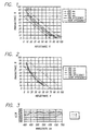
- FIG. 1 shows the relationship between reflectance and transmittance for a number of partial reflectors having the form of thin-film coatings of aluminum deposited on transparent glass substrates, wherein the coatings for the reflectors range in thickness from 1.0 nanometer to 20 nanometers. It will be noted that an increase in the coating's thickness increases the partial reflector's reflectance and decreases its transmittance. It also will be noted that the partial reflectors generally exhibit higher reflectance in red wavelengths than in blue wavelengths and that the reflectors generally have efficiencies in the range of 80 to 90%.
- FIG. 2 shows this same fixed relationship between reflectance and transmittance for partial reflectors in the form of thin-film coatings of chromium deposited on transparent glass substrates. It will be noted that the spectral responses of the chromium reflectors are substantially more uniform, but that they have efficiencies of only about 60% in the middle of the depicted range. Changing the substrates from glass to polymethyl methacrylate has little effect on the depicted relationships.
- Partial reflectors also can be formed by depositing thin-film dielectric coatings onto transparent substrates.
- a partial reflector incorporating a single film of dielectric material e.g., titanium dioxide, with a refractive index at 550 nanometers of about 2.34, deposited on a glass substrate
- Partial reflectors incorporating multiple layers of alternating high-index and low-index dielectric materials can exhibit higher reflectance, with greater spectral uniformity. Again, efficiencies approaching 100% can be achieved.
- FIG. 3 depicts the reflectance and transmittance levels of a partial reflector incorporating a nine-layer dielectric coating.
- the coating incorporates an alternating stack of titanium dioxide and silicon dioxide deposited on a glass substrate. It will be noted that the depicted reflectance and transmittance levels exhibit pronounced maxima and minima as a function of wavelength, with an overall efficiency of about 73%. Multilayer dielectric coatings of yet greater complexity are considered necessary to produce more uniform reflectance and transmittance spectra. This, of course, can lead to higher costs and manufacturing difficulties.
- partial reflectors used in the past have included a three-layer stack deposited on a transparent substrate, in which the stack incorporates an intermediate metal layer (e.g., titanium) sandwiched between an inner layer formed of a material having a relatively high refractive index (e.g., titanium dioxide) and an outer layer formed of a material having a relatively low refractive index (e.g., silicon dioxide).
- an intermediate metal layer e.g., titanium
- an inner layer formed of a material having a relatively high refractive index e.g., titanium dioxide
- an outer layer formed of a material having a relatively low refractive index e.g., silicon dioxide
- US-4,415,233 A discloses a partial reflector in which a multi layer thin film coating is deposited on a surface of a substrate.
- the coating includes a first layer of titanium oxide and zirconium oxide, a second layer which overlies the first layer and is formed of silver metal.
- a third layer overlies the second layer and is formed of a metal oxide.
- a partial reflector comprising a substrate having a front surface and a rear surface; and a multilayer, thin-film coating deposited on one of the surfaces of the substrate, wherein the coating includes a first layer having a prescribed, uniform thickness, wherein the first layer is formed of a prescribed metal oxide, a second layer overlaying the fast layer and having a prescribed, uniform thickness, wherein the second layer is formed of a prescribed metal, and a third layer overlaying the second layer and having a prescribed, unifonn thickness, wherein the third layer is formed of a prescribed metal oxide, wherein the prescribed thicknesses of the first, second and third layers are selected to provide the partial reflector with prescribed reflectance and transmittance values that are substantially uniform over a wavelength band of about 400 to 700 nanometers, and wherein the metal incorporated in the coating's first, second and third layers is the same and consists of niobium, tantalum, titanium, hafnium or zirconium.
- the metal is niobium, in which case the preferred prescribed thickness ranges for the three layers are about 2 to 55 nanometers for the first layer, 3.5 to 36 nanometers for the second layer, and 2 to 60 nanometers for the third layer.
- the refractive indices of the metal oxides that comprise the first and third layers, which sandwich the second, metal layer, are both relatively high, i.e., greater than 2.0.
- FIG. 1 is a graph depicting the relationship between reflectance and transmittance for prior art partial reflectors incorporating thin-film coatings of aluminum deposited on glass substrates.
- FIG. 2 is a graph depicting the relationship between reflectance and transmittance for prior art partial reflectors incorporating thin-film coatings of chromium deposited on glass substrates.
- FIG. 3 is a graph depicting the reflectance and transmittance levels of a prior art partial reflector incorporating a nine-layer dielectric coating deposited on a glass substrate, as such levels vary with wavelength.
- FIG. 4 is a cross-sectional view, not to scale, of a partial reflector embodying the invention, the reflector incorporating a three-layer, thin-film coating deposited on a transparent substrate.
- FIG. 5 is a graph depicting the reflectance and transmittance levels of the partial reflector of Example 1, as such levels vary with wavelength.
- FIG. 6 is a graph depicting the reflectance and transmittance levels of the partial reflector of Example 2, as such levels vary with wavelength.
- FIG. 7 is a graph depicting the reflectance and transmittance levels of the partial reflector of Example 3, as such levels vary with wavelength.
- FIG. 8 is a graph depicting the reflectance and transmittance levels of the partial reflector of Example 4, as such levels vary with wavelength.
- a partial reflector 11 that incorporates a three-layer, thin-film coating 13 deposited on a front surface of a transparent substrate 15.
- the three layers of the coating all incorporate a common metal, and they are configured to facilitate a convenient selection of the partial reflector's desired levels of reflectance, transmittance and efficiency. In addition, this convenient selectability is achieved without the need for a complex or costly manufacturing procedure.
- the back surface of the substrate can carry an optional antireflection or antiglare coating 17, of conventional design.
- the three-layer, thin-film coating 13 incorporates a first, inner layer 19, a second, intermediate layer 21, and a third, outer layer 23.
- the first layer 19 is formed of a metal oxide having a relatively high refractive index, i.e., >2.0.
- the metal incorporated into the first layer is selected from the group consisting of niobium (Nb), tantalum (Ta), titanium (Ti), hafnium (Hf), and zirconium (Zr).
- the second layer 21 is formed only of the same metal as is incorporated into the first layer.
- the third layer 23 is formed of the same metal oxide as is the first layer, again having a relatively high refractive index, i.e., >2.0.
- the first layer 19 of the three-layer coating 13 provides a portion of the partial reflector's desired reflectance, but little or no absorbance.
- the second layer 21 provides a portion of the desired reflectance, but primarily controls the reflector's desired transmittance and efficiency.
- the third layer 23 provides additional tuning of the reflector's optical characteristics, but primarily functions as a protective overcoat.
- the partial reflector's reflectance derives from both constructive interference and metallic conductor reflectance, while its efficiency derives principally from the thickness of the second, metallic layer.
- the transmittance and efficiency of the partial reflector 11 also can be affected by the transparency of the substrate 15.
- Partially absorbing substrates such as 18% grey polymethyl methacrylate (PMMA) and 30% grey PMMA are suitable for use in reducing the reflector's transmittance and efficiency.
- PMMA polymethyl methacrylate
- the actual thicknesses needed for the three layers of the thin-film coating 13 to achieve particular desired levels of reflectance, transmittance and efficiency, can be derived using a suitable computer software program for optical thin-film design. Suitable programs can be obtained from FTG Software Associates, of Princeton, New Jersey, and from Thin Film Center, Inc., of Arlington, Arizona. Such programs can be used to specify the particular thicknesses necessary to achieve these levels, given the layers' specific refractive indices.
- the preferred thickness ranges are 2.0 to 55 nanometers for the first layer 19, 3.5 to 36 nanometers for the second layer 21, and 2.0 to 60 nanometers for the third layer 23.
- reflectances in the range of about 10 to 50%, transmittances in the range of about 5 to 60%, and efficiencies in the range of about 55 to 80% can be achieved.
- Example 1 Example 2
- Example 3 Example 4 First Layer 19 (Nb 2 O 5 thickness, nm) 6.3 35 51 39
- Second Layer 21 (Nb thickness, nm) 8.3 14 8.7 18
- Third Layer 23 (Nb 2 O 5 thickness, nm) 14 11 8 8 Average Reflectance 20.0% 39.7% 39.2% 46.3% Average Transmittance 40.6% 29.8% 39.9% 23.1% Average Efficiency 60.6% 69.5% 79.1% 69.3%
- FIGS. 5-8 depict the reflectance and transmittance levels of the partial reflectors of Examples 1-4, respectively, as a function of wavelength. It will be noted that these levels vary only slightly in the visible wavelength range of 400 to 700 nanometers. The average values for reflectance and transmittance in this wavelength range are set forth in the above Table.
- the partial reflector of Example 1 is configured to provide a transmittance level about twice the reflectance level.
- the reflector of Example 4 is configured to provide an optical performance that is reversed, i.e., a reflectance level about twice the transmittance level.
- the reflector of Example 2 is configured to provide a reflectance of about 40% and a transmittance of about 30%, and the reflector of Example 3 is configured to provide an efficiency of about 80%, with substantially equal levels of reflectance and transmittance.
- the partial reflector 11 of the invention is configured to provide selected levels of reflectance, transmittance and efficiency that are substantially uniform over the entire visible wavelength range of 400 to 700 nanometers. This makes the reflector suitable for use in a wide range of applications, including imaging and information display applications, and laser data retrieval (e.g., CD ROM) applications.
- the partial reflector 11 of the invention is that the three layers 19, 21 and 23 of its thin-film coating 13 all incorporate the same metal. This simplifies the manufacturing process and leads to significant cost savings. For example, if vapor deposition techniques are used, this enables the coating to be conveniently manufactured using just a single sputter target material or a single evaporation material. Similar manufacturing benefits will result if other thin film deposition techniques, e.g., chemical vapor deposition, are used.
- the present invention provides an improved partial reflector that can provide selected levels of reflectance, transmittance and efficiency that are substantially uniform over the visible wavelength range.
- This result is achieved using a special three-layer coating that includes a metal layer sandwiched between two metal oxide dielectric layers having relatively high refractive indices >2.0.
- the three layers all incorporate the same metal, preferably niobium.
Landscapes
- Physics & Mathematics (AREA)
- General Physics & Mathematics (AREA)
- Optics & Photonics (AREA)
- Optical Elements Other Than Lenses (AREA)
- Road Signs Or Road Markings (AREA)
- Aerials With Secondary Devices (AREA)
Claims (6)
- Un réflecteur partiel (11) comprenant :dans lequel les épaisseurs prédéterminées de la première couche (19), de la deuxième couche (21) et de la troisième couche (23) sont choisies pour donner au réflecteur partiel (11) des valeurs prédéterminées de réflectance et de transmittance qui sont sensiblement uniformes sur une bande de longueurs d'onde allant d'environ 400 à 700 nanomètres,un substrat (15) ayant une surface avant et une surface arrière; etun revêtement multicouches (13) en film mince déposé sur l'une des surfaces du substrat, le revêtement (13) comprenantune première couche (19) ayant une épaisseur uniforme prédéterminée, la première couche (19) étant formée d'un oxyde métallique prédéterminé,une deuxième couche (21) recouvrant la première couche et ayant une épaisseur uniforme prédéterminée, la deuxième couche (21) étant formée d'un métal prédéterminé, etune troisième couche (23) recouvrant la deuxième couche (21) et ayant une épaisseur uniforme prédéterminée, la troisième couche (23) étant formée d'un oxyde métallique prédéterminé,
et dans lequel le métal compris dans la première couche (19), la deuxième couche (21) et la troisième couche (23) du revêtement est le même et est constitué de niobium, de tantale, de titanium, d'hafnium ou de zirconium. - Un réflecteur partiel (11) comme défini dans la revendication 1, dans lequel le métal est le niobium.
- Un réflecteur partiel (11) comme défini en revendication 2, dans lequel :l'épaisseur prédéterminée de la première couche (19) est dans la gamme allant d'environ 2 à 55 nanomètres ;l'épaisseur prédéterminée de la deuxième couche (21) est dans la gamme allant d'environ 3,5 à 36 nanomètres ; etl'épaisseur prédéterminée de la troisième couche (23) est dans la gamme allant d'environ 2 à 60 nanomètres.
- Un réflecteur partiel (11) comme défini en revendication 1, dans lequel le revêtement multicouches en film mince (13) comprend uniquement trois couches.
- Un réflecteur partiel (11) comme défini en revendication 1, dans lequel :le revêtement multi-couche (13) en film mince est déposé sur la surface avant (15) du substrat ; etle réflecteur partiel (11) comprend de plus un revêtement anti-réfléchissant (17) déposé sur la surface arrière du substrat.
- Un réflecteur partiel (11) comme défini en revendication 1, dans lequel les indices de réfraction de la première couche (19) et de la troisième couche (23) du revêtement multi-couche (13) sont tous les deux supérieurs à 2,0.
Applications Claiming Priority (3)
| Application Number | Priority Date | Filing Date | Title |
|---|---|---|---|
| US148839 | 1998-09-04 | ||
| US09/148,839 US6231992B1 (en) | 1998-09-04 | 1998-09-04 | Partial reflector |
| PCT/US1999/020094 WO2000014577A1 (fr) | 1998-09-04 | 1999-09-02 | Reflecteur partiel |
Publications (2)
| Publication Number | Publication Date |
|---|---|
| EP1108228A1 EP1108228A1 (fr) | 2001-06-20 |
| EP1108228B1 true EP1108228B1 (fr) | 2002-05-29 |
Family
ID=22527636
Family Applications (1)
| Application Number | Title | Priority Date | Filing Date |
|---|---|---|---|
| EP99945411A Expired - Lifetime EP1108228B1 (fr) | 1998-09-04 | 1999-09-02 | Reflecteur partiel |
Country Status (8)
| Country | Link |
|---|---|
| US (1) | US6231992B1 (fr) |
| EP (1) | EP1108228B1 (fr) |
| JP (1) | JP2002524763A (fr) |
| AT (1) | ATE218212T1 (fr) |
| AU (1) | AU758933B2 (fr) |
| CA (1) | CA2342889A1 (fr) |
| DE (1) | DE69901617T2 (fr) |
| WO (1) | WO2000014577A1 (fr) |
Families Citing this family (35)
| Publication number | Priority date | Publication date | Assignee | Title |
|---|---|---|---|---|
| FR2799005B1 (fr) * | 1999-09-23 | 2003-01-17 | Saint Gobain Vitrage | Vitrage muni d'un empilement de couches minces agissant sur le rayonnement solaire |
| JP2001209038A (ja) * | 1999-11-17 | 2001-08-03 | Nippon Sheet Glass Co Ltd | 液晶表示素子用基板 |
| TW557371B (en) * | 2001-07-02 | 2003-10-11 | Sumitomo Chemical Co | Semi-transparent-semi-reflectivity film, semi- transparent-semi-reflectivity polarized film, polarized light device using these films, and liquid crystal display device using these films |
| US7067195B2 (en) * | 2002-04-29 | 2006-06-27 | Cardinal Cg Company | Coatings having low emissivity and low solar reflectance |
| US7122252B2 (en) | 2002-05-16 | 2006-10-17 | Cardinal Cg Company | High shading performance coatings |
| JP4171970B2 (ja) * | 2002-09-04 | 2008-10-29 | ソニー株式会社 | 投影用スクリーンおよびその製造方法 |
| US7138182B2 (en) * | 2002-07-31 | 2006-11-21 | Cardinal Cg Compay | Temperable high shading performance coatings |
| JP4590847B2 (ja) * | 2003-09-05 | 2010-12-01 | ソニー株式会社 | スクリーン及びその製造方法 |
| US7085059B2 (en) * | 2004-03-24 | 2006-08-01 | Silicon Light Machines Corporation | Spatial light modulator with robust mirror substrate condition |
| US10261321B2 (en) | 2005-11-08 | 2019-04-16 | Lumus Ltd. | Polarizing optical system |
| US20070211257A1 (en) * | 2006-03-09 | 2007-09-13 | Kearl Daniel A | Fabry-Perot Interferometer Composite and Method |
| DE202008011128U1 (de) * | 2008-08-21 | 2010-01-07 | Rehau Ag + Co | Abdeckvorrichtung für ein Leuchtmittel |
| CA2807615C (fr) | 2012-03-08 | 2020-06-30 | Simplehuman, Llc | Miroir de meuble-coiffeuse |
| WO2015131223A1 (fr) * | 2014-03-07 | 2015-09-11 | University Of South Australia | Revêtements décoratifs pour substrats en matière plastique |
| IL235642B (en) | 2014-11-11 | 2021-08-31 | Lumus Ltd | A compact head-up display system is protected by an element with a super-thin structure |
| CA2922596C (fr) | 2015-03-06 | 2023-10-24 | Simplehuman, Llc | Miroir de meuble-lavabo |
| CN109828376B (zh) | 2016-10-09 | 2021-05-18 | 鲁姆斯有限公司 | 使用矩形波导的孔径倍增器 |
| JP6829482B2 (ja) | 2016-11-08 | 2021-02-10 | ルムス エルティーディー. | 光学遮断端部を備えた光ガイド装置およびその製造方法 |
| EP3397998A4 (fr) | 2017-02-22 | 2019-04-17 | Lumus Ltd. | Ensemble optique de guide de lumière |
| US10869537B2 (en) | 2017-03-17 | 2020-12-22 | Simplehuman, Llc | Vanity mirror |
| EP3397997A4 (fr) | 2017-03-22 | 2020-02-12 | Lumus Ltd. | Facettes en chevauchement |
| JP2018165744A (ja) * | 2017-03-28 | 2018-10-25 | セイコーエプソン株式会社 | 導光装置および表示装置 |
| CA3037704A1 (fr) | 2018-03-22 | 2019-09-22 | Simplehuman, Llc | Miroir de meuble-lavabo active par la voix |
| US11526003B2 (en) | 2018-05-23 | 2022-12-13 | Lumus Ltd. | Optical system including light-guide optical element with partially-reflective internal surfaces |
| TWI830753B (zh) * | 2018-07-16 | 2024-02-01 | 以色列商魯姆斯有限公司 | 光導光學元件和用於向觀察者的眼睛提供圖像的顯示器 |
| EP3931615A1 (fr) | 2019-03-01 | 2022-01-05 | Simplehuman LLC | Miroir de courtoisie |
| CN114072717A (zh) | 2019-06-27 | 2022-02-18 | 鲁姆斯有限公司 | 基于经由光导光学元件对眼睛成像来进行眼睛追踪的设备和方法 |
| IL270991B (en) | 2019-11-27 | 2020-07-30 | Lumus Ltd | A light guide with an optical element to perform polarization mixing |
| CN114746797A (zh) | 2019-12-08 | 2022-07-12 | 鲁姆斯有限公司 | 具有紧凑型图像投影仪的光学系统 |
| TW202235772A (zh) | 2020-11-09 | 2022-09-16 | 以色列商魯姆斯有限公司 | Ar系統中顏色校正的背反射 |
| WO2022180634A1 (fr) | 2021-02-25 | 2022-09-01 | Lumus Ltd. | Multiplicateurs à ouverture optique ayant un guide d'ondes rectangulaire |
| TW202244552A (zh) | 2021-03-01 | 2022-11-16 | 以色列商魯姆斯有限公司 | 具有從投影儀到波導中的緊湊耦合的光學系統 |
| KR20230133841A (ko) | 2021-05-19 | 2023-09-19 | 루머스 리미티드 | 액티브 광학 엔진 |
| TW202307518A (zh) | 2021-07-04 | 2023-02-16 | 以色列商魯姆斯有限公司 | 具有提供視場的不同部分的堆疊光導元件的顯示器 |
| TW202309570A (zh) | 2021-08-23 | 2023-03-01 | 以色列商魯姆斯有限公司 | 具有嵌入式耦入反射器的複合光導光學元件的製造方法 |
Family Cites Families (33)
| Publication number | Priority date | Publication date | Assignee | Title |
|---|---|---|---|---|
| US3673981A (en) | 1969-05-13 | 1972-07-04 | Libbey Owens Ford Co | Filming apparatus |
| US3826728B2 (en) | 1970-05-20 | 1994-07-12 | Boc Group Plc | Transparent article having reduced solar radiation transmittance and method of making same |
| US4337990A (en) | 1974-08-16 | 1982-07-06 | Massachusetts Institute Of Technology | Transparent heat-mirror |
| US4721349A (en) | 1974-08-16 | 1988-01-26 | Massachusetts Institute Of Technology | Transparent heat-mirror |
| US4022947A (en) | 1975-11-06 | 1977-05-10 | Airco, Inc. | Transparent panel having high reflectivity for solar radiation and a method for preparing same |
| US4556277A (en) | 1976-05-27 | 1985-12-03 | Massachusetts Institute Of Technology | Transparent heat-mirror |
| JPS57130001A (en) | 1981-02-05 | 1982-08-12 | Canon Inc | Low polalization achromatic beam splitter |
| US4932754A (en) | 1983-10-07 | 1990-06-12 | U.S. Philips Corp. | Multilayer optical component |
| US4822748A (en) | 1984-08-20 | 1989-04-18 | California Institute Of Technology | Photosensor with enhanced quantum efficiency |
| FR2570392B1 (fr) | 1984-09-19 | 1987-01-02 | Dme | Procede de depot sur substrats optiques de couches antireflechissantes susceptibles d'etre gravees |
| US4773717A (en) | 1986-11-03 | 1988-09-27 | Ovonic Synthetic Materials Co. | Transparency having a second surface multilayer decorative coating |
| US4931315A (en) | 1986-12-17 | 1990-06-05 | Gte Products Corporation | Wide angle optical filters |
| DE3818341C2 (de) | 1987-06-04 | 1993-10-28 | Olympus Optical Co | Teildurchlässiger Spiegel aus Kunststoff |
| US4904083A (en) | 1987-09-11 | 1990-02-27 | Litton Systems, Inc. | Partially transparent mirror for a ring laser |
| GB8821116D0 (en) | 1988-09-08 | 1989-11-08 | Barr & Stroud Ltd | Infra-red transmitting optical components and optical coatings therefor |
| US5198930A (en) | 1989-02-14 | 1993-03-30 | Kabushiki Kaisha Topcon | Wide-band half-mirror |
| US5055358A (en) | 1989-09-29 | 1991-10-08 | Libbey-Owens-Ford Co. | Low reflectance films for transparent substrates |
| US5216551A (en) | 1990-02-16 | 1993-06-01 | Asahi Kogaku Kogyo K.K. | Surface reflector |
| US5194989A (en) | 1990-05-07 | 1993-03-16 | Mcdonnell Douglas Corporation | Dielectric combiner including first and second dielectric materials having indices of refraction greater than 2.0 |
| US5419969A (en) | 1990-07-05 | 1995-05-30 | Asahi Glass Company Ltd. | Low emissivity film |
| SG47839A1 (en) | 1990-07-05 | 1998-04-17 | Asahi Glass Co Ltd | A low emissivity film |
| US5532062A (en) | 1990-07-05 | 1996-07-02 | Asahi Glass Company Ltd. | Low emissivity film |
| JPH05502310A (ja) | 1990-08-30 | 1993-04-22 | バイラテック・シン・フィルムズ・インコーポレイテッド | 酸化ニオブを含むdc反応性スパッタリングされた光学被覆 |
| US5140457A (en) | 1990-11-13 | 1992-08-18 | Bausch & Lomb Incorporated | Reflector for display lighting |
| US5171414A (en) | 1990-12-10 | 1992-12-15 | Ford Motor Company | Method of making transparent anti-reflective coating |
| US5306547A (en) * | 1990-12-14 | 1994-04-26 | Southwall Technologies Inc. | Low transmission heat-reflective glazing materials |
| SG54312A1 (en) * | 1991-04-30 | 1998-11-16 | Saint Gobain Vitrage | Glass substrate coated with thin multifilms for protection against solar radiation |
| JPH0728999Y2 (ja) | 1991-05-29 | 1995-07-05 | セントラル硝子株式会社 | 多色表示ヘッドアップディスプレイ用ガラス |
| GB2268509B (en) | 1992-07-11 | 1996-01-31 | Pilkington Uk Ltd | Coatings on glass |
| US5521759A (en) | 1993-06-07 | 1996-05-28 | National Research Council Of Canada | Optical filters for suppressing unwanted reflections |
| US5510173A (en) | 1993-08-20 | 1996-04-23 | Southwall Technologies Inc. | Multiple layer thin films with improved corrosion resistance |
| US5808714A (en) * | 1993-09-30 | 1998-09-15 | Optical Coating Laboratory, Inc. | Low reflection shadow mask |
| DE19541937C1 (de) * | 1995-11-10 | 1996-11-28 | Ver Glaswerke Gmbh | Wärmedämmendes Schichtsystem mit niedriger Emissivität, hoher Transmission und neutraler Ansicht in Reflexion und Transmission |
-
1998
- 1998-09-04 US US09/148,839 patent/US6231992B1/en not_active Expired - Fee Related
-
1999
- 1999-09-02 DE DE69901617T patent/DE69901617T2/de not_active Expired - Fee Related
- 1999-09-02 AT AT99945411T patent/ATE218212T1/de not_active IP Right Cessation
- 1999-09-02 JP JP2000569266A patent/JP2002524763A/ja active Pending
- 1999-09-02 AU AU58014/99A patent/AU758933B2/en not_active Ceased
- 1999-09-02 WO PCT/US1999/020094 patent/WO2000014577A1/fr active IP Right Grant
- 1999-09-02 CA CA002342889A patent/CA2342889A1/fr not_active Abandoned
- 1999-09-02 EP EP99945411A patent/EP1108228B1/fr not_active Expired - Lifetime
Also Published As
| Publication number | Publication date |
|---|---|
| CA2342889A1 (fr) | 2000-03-16 |
| WO2000014577A1 (fr) | 2000-03-16 |
| DE69901617T2 (de) | 2002-11-21 |
| DE69901617D1 (de) | 2002-07-04 |
| AU758933B2 (en) | 2003-04-03 |
| AU5801499A (en) | 2000-03-27 |
| EP1108228A1 (fr) | 2001-06-20 |
| US6231992B1 (en) | 2001-05-15 |
| JP2002524763A (ja) | 2002-08-06 |
| ATE218212T1 (de) | 2002-06-15 |
Similar Documents
| Publication | Publication Date | Title |
|---|---|---|
| EP1108228B1 (fr) | Reflecteur partiel | |
| US5337191A (en) | Broad band pass filter including metal layers and dielectric layers of alternating refractive index | |
| US6034813A (en) | Wavelength selective applied films with glare control | |
| JP2561946B2 (ja) | 多層膜裏面反射鏡 | |
| US5450238A (en) | Four-layer antireflection coating for deposition in in-like DC sputtering apparatus | |
| JP3446833B2 (ja) | 導電性光減衰反射防止被覆およびそれを施した物品 | |
| JP2887530B2 (ja) | 車両特に自動車用バックミラー | |
| US5140457A (en) | Reflector for display lighting | |
| US3463574A (en) | Multilayer antireflection coating for low index materials | |
| JPH05503372A (ja) | D.c.反応性スパッタリングされた反射防止被覆 | |
| JPH05502310A (ja) | 酸化ニオブを含むdc反応性スパッタリングされた光学被覆 | |
| JPH02120801A (ja) | 多層膜表面反射鏡 | |
| JPH0875902A (ja) | 多層反射防止膜 | |
| JP2566634B2 (ja) | 多層反射防止膜 | |
| JPS63134232A (ja) | 高透過率を有する赤外反射物品 | |
| JPS6015604A (ja) | 自動車用反射鏡 | |
| JP3550894B2 (ja) | 反射防止膜 | |
| JP2746602B2 (ja) | 分光フイルター | |
| JP2561947B2 (ja) | 多層膜裏面反射鏡 | |
| KR100430024B1 (ko) | 선택성 칼라를 형성하는 다층박막 안경렌즈 및 칼라를제어하는 방법 | |
| JPS5929841B2 (ja) | ガラスレンズにコスメテイツク・カラ−・コ−テイングした光学部材 | |
| JPH1130705A (ja) | 反射防止膜を有する眼鏡プラスチックレンズ | |
| JPH0419521B2 (fr) | ||
| JPH06250001A (ja) | 多層反射防止膜およびそれが施された光学系 | |
| JPH03116101A (ja) | 合成樹脂製光学物品の反射防止膜 |
Legal Events
| Date | Code | Title | Description |
|---|---|---|---|
| PUAI | Public reference made under article 153(3) epc to a published international application that has entered the european phase |
Free format text: ORIGINAL CODE: 0009012 |
|
| 17P | Request for examination filed |
Effective date: 20010404 |
|
| AK | Designated contracting states |
Kind code of ref document: A1 Designated state(s): AT BE CH CY DE DK ES FI FR GB GR IE IT LI LU MC NL PT SE |
|
| GRAG | Despatch of communication of intention to grant |
Free format text: ORIGINAL CODE: EPIDOS AGRA |
|
| 17Q | First examination report despatched |
Effective date: 20010723 |
|
| GRAG | Despatch of communication of intention to grant |
Free format text: ORIGINAL CODE: EPIDOS AGRA |
|
| GRAG | Despatch of communication of intention to grant |
Free format text: ORIGINAL CODE: EPIDOS AGRA |
|
| GRAH | Despatch of communication of intention to grant a patent |
Free format text: ORIGINAL CODE: EPIDOS IGRA |
|
| GRAH | Despatch of communication of intention to grant a patent |
Free format text: ORIGINAL CODE: EPIDOS IGRA |
|
| GRAA | (expected) grant |
Free format text: ORIGINAL CODE: 0009210 |
|
| AK | Designated contracting states |
Kind code of ref document: B1 Designated state(s): AT BE CH CY DE DK ES FI FR GB GR IE IT LI LU MC NL PT SE |
|
| PG25 | Lapsed in a contracting state [announced via postgrant information from national office to epo] |
Ref country code: GR Free format text: LAPSE BECAUSE OF FAILURE TO SUBMIT A TRANSLATION OF THE DESCRIPTION OR TO PAY THE FEE WITHIN THE PRESCRIBED TIME-LIMIT Effective date: 20020529 Ref country code: FI Free format text: LAPSE BECAUSE OF FAILURE TO SUBMIT A TRANSLATION OF THE DESCRIPTION OR TO PAY THE FEE WITHIN THE PRESCRIBED TIME-LIMIT Effective date: 20020529 Ref country code: BE Free format text: LAPSE BECAUSE OF FAILURE TO SUBMIT A TRANSLATION OF THE DESCRIPTION OR TO PAY THE FEE WITHIN THE PRESCRIBED TIME-LIMIT Effective date: 20020529 Ref country code: AT Free format text: LAPSE BECAUSE OF FAILURE TO SUBMIT A TRANSLATION OF THE DESCRIPTION OR TO PAY THE FEE WITHIN THE PRESCRIBED TIME-LIMIT Effective date: 20020529 |
|
| REF | Corresponds to: |
Ref document number: 218212 Country of ref document: AT Date of ref document: 20020615 Kind code of ref document: T |
|
| REG | Reference to a national code |
Ref country code: GB Ref legal event code: FG4D |
|
| REG | Reference to a national code |
Ref country code: CH Ref legal event code: NV Representative=s name: ISLER & PEDRAZZINI AG Ref country code: CH Ref legal event code: EP |
|
| REG | Reference to a national code |
Ref country code: IE Ref legal event code: FG4D |
|
| REF | Corresponds to: |
Ref document number: 69901617 Country of ref document: DE Date of ref document: 20020704 |
|
| ET | Fr: translation filed | ||
| PG25 | Lapsed in a contracting state [announced via postgrant information from national office to epo] |
Ref country code: SE Free format text: LAPSE BECAUSE OF FAILURE TO SUBMIT A TRANSLATION OF THE DESCRIPTION OR TO PAY THE FEE WITHIN THE PRESCRIBED TIME-LIMIT Effective date: 20020829 Ref country code: PT Free format text: LAPSE BECAUSE OF FAILURE TO SUBMIT A TRANSLATION OF THE DESCRIPTION OR TO PAY THE FEE WITHIN THE PRESCRIBED TIME-LIMIT Effective date: 20020829 Ref country code: DK Free format text: LAPSE BECAUSE OF FAILURE TO SUBMIT A TRANSLATION OF THE DESCRIPTION OR TO PAY THE FEE WITHIN THE PRESCRIBED TIME-LIMIT Effective date: 20020829 |
|
| PG25 | Lapsed in a contracting state [announced via postgrant information from national office to epo] |
Ref country code: LU Free format text: LAPSE BECAUSE OF NON-PAYMENT OF DUE FEES Effective date: 20020902 Ref country code: IE Free format text: LAPSE BECAUSE OF NON-PAYMENT OF DUE FEES Effective date: 20020902 |
|
| PG25 | Lapsed in a contracting state [announced via postgrant information from national office to epo] |
Ref country code: CY Free format text: LAPSE BECAUSE OF FAILURE TO SUBMIT A TRANSLATION OF THE DESCRIPTION OR TO PAY THE FEE WITHIN THE PRESCRIBED TIME-LIMIT Effective date: 20020930 |
|
| PG25 | Lapsed in a contracting state [announced via postgrant information from national office to epo] |
Ref country code: ES Free format text: LAPSE BECAUSE OF FAILURE TO SUBMIT A TRANSLATION OF THE DESCRIPTION OR TO PAY THE FEE WITHIN THE PRESCRIBED TIME-LIMIT Effective date: 20021128 |
|
| PG25 | Lapsed in a contracting state [announced via postgrant information from national office to epo] |
Ref country code: MC Free format text: LAPSE BECAUSE OF NON-PAYMENT OF DUE FEES Effective date: 20030401 |
|
| PLBE | No opposition filed within time limit |
Free format text: ORIGINAL CODE: 0009261 |
|
| STAA | Information on the status of an ep patent application or granted ep patent |
Free format text: STATUS: NO OPPOSITION FILED WITHIN TIME LIMIT |
|
| 26N | No opposition filed |
Effective date: 20030303 |
|
| REG | Reference to a national code |
Ref country code: IE Ref legal event code: MM4A |
|
| PGFP | Annual fee paid to national office [announced via postgrant information from national office to epo] |
Ref country code: NL Payment date: 20040816 Year of fee payment: 6 |
|
| PGFP | Annual fee paid to national office [announced via postgrant information from national office to epo] |
Ref country code: GB Payment date: 20040825 Year of fee payment: 6 |
|
| PGFP | Annual fee paid to national office [announced via postgrant information from national office to epo] |
Ref country code: FR Payment date: 20040920 Year of fee payment: 6 |
|
| PGFP | Annual fee paid to national office [announced via postgrant information from national office to epo] |
Ref country code: CH Payment date: 20040924 Year of fee payment: 6 |
|
| PGFP | Annual fee paid to national office [announced via postgrant information from national office to epo] |
Ref country code: DE Payment date: 20041102 Year of fee payment: 6 |
|
| PG25 | Lapsed in a contracting state [announced via postgrant information from national office to epo] |
Ref country code: IT Free format text: LAPSE BECAUSE OF NON-PAYMENT OF DUE FEES;WARNING: LAPSES OF ITALIAN PATENTS WITH EFFECTIVE DATE BEFORE 2007 MAY HAVE OCCURRED AT ANY TIME BEFORE 2007. THE CORRECT EFFECTIVE DATE MAY BE DIFFERENT FROM THE ONE RECORDED. Effective date: 20050902 Ref country code: GB Free format text: LAPSE BECAUSE OF NON-PAYMENT OF DUE FEES Effective date: 20050902 |
|
| PG25 | Lapsed in a contracting state [announced via postgrant information from national office to epo] |
Ref country code: LI Free format text: LAPSE BECAUSE OF NON-PAYMENT OF DUE FEES Effective date: 20050930 Ref country code: CH Free format text: LAPSE BECAUSE OF NON-PAYMENT OF DUE FEES Effective date: 20050930 |
|
| PG25 | Lapsed in a contracting state [announced via postgrant information from national office to epo] |
Ref country code: NL Free format text: LAPSE BECAUSE OF NON-PAYMENT OF DUE FEES Effective date: 20060401 Ref country code: DE Free format text: LAPSE BECAUSE OF NON-PAYMENT OF DUE FEES Effective date: 20060401 |
|
| REG | Reference to a national code |
Ref country code: CH Ref legal event code: PL |
|
| GBPC | Gb: european patent ceased through non-payment of renewal fee |
Effective date: 20050902 |
|
| PG25 | Lapsed in a contracting state [announced via postgrant information from national office to epo] |
Ref country code: FR Free format text: LAPSE BECAUSE OF NON-PAYMENT OF DUE FEES Effective date: 20060531 |
|
| NLV4 | Nl: lapsed or anulled due to non-payment of the annual fee |
Effective date: 20060401 |
|
| REG | Reference to a national code |
Ref country code: FR Ref legal event code: ST Effective date: 20060531 |