EP1090334B1 - System and method for controlling a multi-arm polishing tool - Google Patents
System and method for controlling a multi-arm polishing tool Download PDFInfo
- Publication number
- EP1090334B1 EP1090334B1 EP98964086A EP98964086A EP1090334B1 EP 1090334 B1 EP1090334 B1 EP 1090334B1 EP 98964086 A EP98964086 A EP 98964086A EP 98964086 A EP98964086 A EP 98964086A EP 1090334 B1 EP1090334 B1 EP 1090334B1
- Authority
- EP
- European Patent Office
- Prior art keywords
- arm
- polishing
- downforce
- polish
- run
- Prior art date
- Legal status (The legal status is an assumption and is not a legal conclusion. Google has not performed a legal analysis and makes no representation as to the accuracy of the status listed.)
- Expired - Lifetime
Links
Images
Classifications
-
- G—PHYSICS
- G05—CONTROLLING; REGULATING
- G05B—CONTROL OR REGULATING SYSTEMS IN GENERAL; FUNCTIONAL ELEMENTS OF SUCH SYSTEMS; MONITORING OR TESTING ARRANGEMENTS FOR SUCH SYSTEMS OR ELEMENTS
- G05B19/00—Programme-control systems
- G05B19/02—Programme-control systems electric
- G05B19/418—Total factory control, i.e. centrally controlling a plurality of machines, e.g. direct or distributed numerical control [DNC], flexible manufacturing systems [FMS], integrated manufacturing systems [IMS] or computer integrated manufacturing [CIM]
- G05B19/41815—Total factory control, i.e. centrally controlling a plurality of machines, e.g. direct or distributed numerical control [DNC], flexible manufacturing systems [FMS], integrated manufacturing systems [IMS] or computer integrated manufacturing [CIM] characterised by the cooperation between machine tools, manipulators and conveyor or other workpiece supply system, workcell
-
- B—PERFORMING OPERATIONS; TRANSPORTING
- B25—HAND TOOLS; PORTABLE POWER-DRIVEN TOOLS; MANIPULATORS
- B25J—MANIPULATORS; CHAMBERS PROVIDED WITH MANIPULATION DEVICES
- B25J9/00—Programme-controlled manipulators
- B25J9/16—Programme controls
- B25J9/1656—Programme controls characterised by programming, planning systems for manipulators
- B25J9/1669—Programme controls characterised by programming, planning systems for manipulators characterised by special application, e.g. multi-arm co-operation, assembly, grasping
-
- Y—GENERAL TAGGING OF NEW TECHNOLOGICAL DEVELOPMENTS; GENERAL TAGGING OF CROSS-SECTIONAL TECHNOLOGIES SPANNING OVER SEVERAL SECTIONS OF THE IPC; TECHNICAL SUBJECTS COVERED BY FORMER USPC CROSS-REFERENCE ART COLLECTIONS [XRACs] AND DIGESTS
- Y02—TECHNOLOGIES OR APPLICATIONS FOR MITIGATION OR ADAPTATION AGAINST CLIMATE CHANGE
- Y02P—CLIMATE CHANGE MITIGATION TECHNOLOGIES IN THE PRODUCTION OR PROCESSING OF GOODS
- Y02P90/00—Enabling technologies with a potential contribution to greenhouse gas [GHG] emissions mitigation
- Y02P90/02—Total factory control, e.g. smart factories, flexible manufacturing systems [FMS] or integrated manufacturing systems [IMS]
Definitions
- the present invention relates generally to the planarization of semiconductor wafers and, more specifically, to a system and method for controlling a polishing tool having multiple arms.
- Chemical-mechanical polishing is a widely used means of planarizing silicon dioxide as well as other types of layers on semiconductor wafers.
- Chemical mechanical polishing typically utilizes an abrasive slurry disbursed in an alkaline or acidic solution to planarize the surface of the wafer through a combination of mechanical and chemical action.
- a typical chemical mechanical polishing tool includes a rotatable circular platen or table on which a polishing pad is mounted and a polishing device is positioned above the pad.
- the polishing device includes one or more rotating carrier heads to which wafers can be secured typically through the use of vacuum pressure.
- the platen is rotated and an abrasive slurry is disbursed onto the polishing pad.
- a downforce is applied to each rotating carrier head to press its wafer against the polishing pad. As the wafer is pressed against the polishing pad, the surface of the wafer is mechanically and chemically polished.
- EP-A-0 770 455 discloses a conditioner apparatus for a chemical mechanical polishing system.
- the disclosure relates to a conditioner apparatus which uses one or more linear conditioners.
- the linear conditioners extend from the edge of the polishing pad almost to the center of the pad.
- the conditioner apparatus may use about a radial axis two conditioner rods located on either side of radial segment.
- the rods gimbal so that if one rod rises, the other rod is forced downwardly.
- the rods can pivot independently about a lateral axis, but they cannot pivot around the vertical axis.
- the linear conditioners may be actuated by a piezoelectric member or swept by an arm towards and away from the center of the polishing pad.
- US 5 653 622 discloses a chemical mechanical polishing system for processing semiconductor wafers has a polishing arm and carrier assembly that press the topside surface of a semiconductor wafer against a motor driven, rotating polishing pad. Improved uniformity of material removal, as well as improved stability of material removal rate, is achieved through the use of a controller that applies a variable wafer backside pressure to the wafers being polished. More specifically, a control subsystem maintains a wafer count, corresponding to how many wafers have been polished by the polishing pad. The control subsystem regulates the backside pressure applied to each wafer in accordance with a predetermined function such that the backside pressure increases monotonically as the wafer count increases.
- US 5 665 199 discloses a method for developing and characterizing a polish process for polishing an interlayer dielectric (ILD) layer for a specific product or a specific patterned metal layer is provided.
- a statistically-based model for ILD planarization by chemical mechanical polish (CMP) is used as a guide to determine, in an empirical manner, the proper amount of ILD polishing that will be required to planarize an ILD layer.
- CMP chemical mechanical polish
- the statistically-based model also shows the resulting ILD thicknesses to be expected.
- the ILD deposition thickness can be adjusted to attain the desired planarized ILD thickness.
- the attainment of local planarity must be confirmed by an independent measurement technique.
- the polish process development methodology is extendible with respect to minimum interconnect feature size. This polish process development methodology can also be applied to products requiring multiple planarizations for multiple levels of interconnects.
- the present invention provides a system and method of controlling a polishing tool having multiple arms.
- the present invention provides a method of controlling a polishing tool having multiple arms, the method comprising:
- the present invention provides a controller for controlling a polishing tool having multiple arms, the controller comprising:
- the present invention generally provides a system and method for controlling a polishing tool having multiple arms.
- the invention in particular, provides techniques for controlling the removal rate of each arm taking into account the downforces applied by each of the arms. In this manner, removal rate variations between arms and between wafers can be reduced. While the invention is not so limited, a more thorough understanding of the invention will be achieved by reading the detailed description which follows.
- the exemplary polishing tool 100 generally includes a polishing pad 110 mounted on a platen 112 and a multi-head carrier 120 positioned above the polishing pad 110.
- the multi-head carrier 120 typically includes a plurality of rotatable polishing arms 122, each of which includes a head 124. Wafers can be secured to the carrier heads 124 by known techniques such as vacuum pressure.
- a source of polishing fluid (not shown) is also provided to supply polishing fluid to the pad 110 for polishing.
- the polishing tool 100 is illustrated by way of example only.
- the illustration of a five arm polishing tool is also provided by way of example.
- the invention extends to cover the control of any multiple arm polishing tool having more than one arm.
- the platen 112 is rotated at a typically constant table speed and downforces are applied to each of the polishing arms for a predetermined time, based on expected removal rates.
- the post-polishing thickness of the polished layers are measured and compared against a target post-polish thickness.
- the polishing tool is taken out of production and the downforces on the arms are adjusted. These adjustments are determined by running a series of monitor wafers on the tool and applying different downforces on the arms to determine the removal rate of an individual arm based on the downforce applied to the individual arm. Then, the downforce on each arm is independently adjusted in attempt to re-center the process.
- Figure 2 is an exemplary graph depicting removal rate variations across the arms of a five-arm polishing tool using conventional polishing techniques. Specifically, Figure 2 depicts the range and standard deviation of removal rates of the arms as a function of lot number. As can be seen, for a given wafer lot, removal rates between the arms can vary up to about 7 angstroms/second with a standard deviation of about 3 angstroms per second.
- the present invention provides polish tool control techniques which account for arm-to-arm interaction and which can, for example, reduce arm-to-arm removal rate variations.
- the interaction between the arms of a polishing tool having N arms may be modeled by the following relationship: Where j represents a polish arm, ⁇ x represents the amount of material removed on the wafer of arm j, ⁇ t represents the polish time, R j represents the removal rate for polish arm j, ⁇ F i represents the downforce adjustment (from a nominal downforce) for polish arm i and K i is a coefficient for polish arm i relating the downforce adjustment of polishing arm i ( ⁇ F i ) to the removal rate for polishing arm j (R j ).
- R k+1 R k +K ⁇ F k
- R k+1 is a vector representing the removal rates at each arm for a run k+1
- vector R k represents the removal rates for each arm at run k
- ⁇ F k is a vector representing the downforce adjustments for the arms
- the coefficient matrix K defines the relationship between removal rate changes (R k+1 -R k ) and downforce adjustments ⁇ F k .
- run identifies a group of one or more batches of wafers which are polished using the same downforce adjustments.
- wafer batch refers to a group of wafers loaded onto a polish arm.
- a wafer batch may include production as well as nonproduction wafers.
- the above process model advantageously takes into account the downforce adjustments on all of the arms in determining the change in removal rate for each arm and, in this manner, accounts for the interaction between the polishing arms.
- FIG. 3 illustrates an exemplary system for controlling a polish tool having multiple arms.
- the exemplary system 300 includes two metrology tools 310 and 312 for measuring pre-polish thicknesses and post-polish thicknesses of wafer layers (e.g., dielectric layers), respectively. It should be appreciated that while two metrology tools are illustrated, a single metrology tool may be used to perform both pre- and post-polish thickness measurements.
- the two metrology tools 310 and 312 are coupled to a polish tool 320.
- a suitable metrology tool for many applications is the Optiprobe metrology tool by Therma-Wave, Inc..
- the system further includes a controller 330 coupled to the polishing tool 320 for controlling the polishing tool.
- the controller 330 generally receives pre- and post-polish thickness measurements from the metrology tools 310 and 312 and uses the thickness measurements to control the polish tool 320.
- the exemplary controller 330 includes an "out of control" module (OOC module) 332 for determining when downforce adjustments to the polish tool 320 are needed, and an optimizer module 334 which, when the tool moves out of control, determines new downforce adjustments for the polish tool 320 using nonproduction wafer thickness data.
- OOC module "out of control” module”
- the controller may, for example, be a model predictive controller implemented using, for example, MatLab Optimization Toolbox® routines.
- the controller 330 may be interfaced with the polish tool 320 using, for example, an Advance Process Control Framework interface.
- FIG. 4 An exemplary process flow for the system 300 is illustrated in Figure 4.
- this exemplary process will be illustrated using a five-arm polish tool 320.
- a first wafer batch e.g., five wafers for a five arm polish tool
- the pre-polish thicknesses are provided to the controller 330 and typically stored thereby.
- the batch of wafers is then loaded onto the carrier heads of the tool's polishing arms and the wafer batch is polished using a predetermined downforce adjustment for each arm, as indicated at block 404.
- the downforce adjustments may be either calculated by the optimizer module 334 at block 412 (as will be discussed below) or, for an initial run, predefined by an operator.
- the polishing is typically performed at a predetermined table speed and a selected time which, based on expected removal rate, provides for removal of a predetermined amount of material.
- the expected removal rate may be a mean predicted removal rate for the arms calculated by the optimizer module 334 (e.g., at block 412) and input to the polish tool 320.
- the post-polish thicknesses of the wafer batch are determined and provided to the controller 320.
- the OOC module 332 determines whether the polish process is out of control. In the illustrated embodiment, this is done by determining, for each arm, a difference between the post-polish thickness for the wafer of the arm and a target thickness and updating a cumulative sum (CUSUM) for the arm with the difference, as indicated at block 408. The OCC module 332 then checks to determine whether the CUSUM for any arm exceeds a predetermined threshold as indicated at block 410. If not, control moves to block 402 and another wafer batch is processed using the same downforce adjustments.
- CUSUM cumulative sum
- control moves to block 412 where the optimizer module 334 determines new downforce adjustments (which will be applied to a subsequent production wafer run) for the arms using nonproduct test wafers.
- the CUSUM for each arm is also reset.
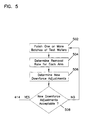
- a mean predicted removal rate for the subsequent wafer run may also be determined using the new downforce adjustments. Details of block 410 are illustrated in Figure 5.
- Control then moves to block 414 where the new downforce adjustments are provided to the polish tool 320.
- the mean predicted removal rate may also be provided to the polish tool 320 so the tool may calculate a polish time.
- Another wafer batch is then processed using downforces adjusted by the downforce adjustments determined by the optimizer module 334 at block 412.
- Figure 5 illustrates an exemplary process flow for determining downforce adjustments using test wafers.
- the test wafers may, for example, be bare silicon wafers with a relatively thick (e.g., 20,000 Angstrom) blanket layer of oxide on top.
- one or more batches of test wafers are polished.
- the removal rate for each arm is then determined, as indicated at block 504. This is done using pre- and post-polish thickness measurements for the test wafer batch(es) and the polish time for each wafer batch.
- the removal rate of a given arm may simply be the difference in post- and pre-polish thickness for the wafer polished by the arm divided by the polish time.
- the polish time may be provided to the controller 320 from the polish tool 320.
- an average removal rate for each arm is determined.
- new downforce adjustments for the arms are determined, as indicated at block 506.
- the optimizer module 334 solves an optimization equation using the removal rates determined at block 504 and a relationship between arm removal rates and arm downforce adjustments. Details of an exemplary optimization equation are discussed below.
- the new downforce adjustments may now be used for polishing production wafer batches.
- a verification batch of test wafers is polished using the new downforce adjustments to verify a return to an "in-control" state. The verification may be performed by determining whether the difference between the post-polish thickness of any verification batch wafer layer and an expected thickness falls below a predetermined threshold. If not, control moves to block 414, where the new downforce adjustments are provided to the polish tool 320 for polishing a subsequent production wafer run. Otherwise, control returns to block 502 to recalculate new downforce adjustments.
- the new downforce adjustments are determined by solving an optimization equation.
- the optimization equation is typically dependent upon downforce adjustments and removal rates.
- the optimization equation [3] above may be solved to minimize the variation in predicted removal rates for run k+1 across the polish arms using the mean of the removal rates at run k as the desired mean removal rates for run k+1.
- the downforce adjustments are determined using the optimization equation [3] subject to the process model [2] and operational constraints.
- the coefficient matrix K can vary depending on the polishing tool as well as the layer being polished.
- a coefficient matrix K may be determined using test wafers.
- test wafers e.g., bare silicon wafers with approximately 20,000 angstroms of deposited oxide
- This may be done by polishing a number of test wafer batches with a variety of downforce adjustments on each of the polishing arms and determining arm removal rates as a function of downforce adjustments using known techniques.
- One suitable technique includes using the auto-regressive with exogenous inputs (arx) modeling function provided in the MatLabTM system identification tool box.
- Figure 6 is an exemplary graph illustrating the performance benefits of the control system and process illustrated in Figures 3-5 as compared to conventional controller techniques. Specifically, Figure 6 shows the reduction in removal rate variation range and the reduction in standard deviation when using the control system and process illustrated in Figures 3-5 as compared to conventional controller techniques. As can be seen, the above described control system and process reduced both the range and standard deviation of removal rates for each trial. While the results were varied due to the large natural variation in the process, improvements were shown in each trial. In some, an average reduction of 42% in both range and standard deviation was seen over the 13 trial.
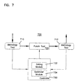
- Figure 7 illustrates another exemplary system for controlling a polish tool having multiple arms.
- the exemplary system 700 advantageously use production wafer data rather than test wafer data for controlling the downforce adjustment for each arm of a polish tool.
- the system 700 includes two metrology tools 710 and 712, coupled to a polish tool 720, for measuring pre-polish thicknesses and post-polish thicknesses, respectively.
- the system 700 further includes a controller 730 coupled to the polishing tool 720 for controlling the polishing tool based on production wafer thickness data.
- the controller 730 generally receives pre- and post-polish thickness measurements of production wafers from the metrology tools 710 and 712 and uses these thickness measurements to control the polish tool 720.
- the exemplary controller 730 may include a gating module 732 for determining when to adjust downforces of the polishing arms on the tool 720, and an optimizer module 734 which, when allowed by the gating module, determines downforce adjustments for the processing tool 720 based on production wafer thickness data.
- the controller 720 may, for example, be a model predictive controller implemented using, for example, MatLab Optimization Toolbox® routines and an Advance Process Control Framework interface.
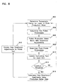
- a topology factor for each wafer layer of a first wafer batch (e.g., five wafers for a five arm polish tool) is provided to the controller 730.
- the topology factor is a predetermined factor associated with each layer of a wafer which accounts for different coefficient matrices K for each wafer layer as compared to test wafers.
- the first wafer batch is provided to the metrology tool 610 for measuring pre-polish thicknesses of the wafer layers to be polished. The pre-polish thicknesses are provided to the controller 730.
- the batch of wafers is then loaded onto the carrier heads of the tool's polishing arms and the wafers are polished using a downforce adjustment for each arm, as indicated at block 806.
- the downforce adjustments may either be calculated by the optimizer module 734 at block 814 (as will be discussed below) or, for an initial run, predefined, for example, by an operator.
- the polishing is typically performed at a predetermined table speed and a selected time which, based on expected removal rate, provides for removal of a predetermined amount of material.
- the expected removal rate may be a mean predicted removal rate calculated by the optimizer module 734 (e.g., at block 814) and input to the polish tool 720.
- the post-polish thicknesses of the wafer batch are determined and provided to the controller 720.
- the gating module 722 uses the post and pre-polish thickness data, the gating module 722 updates a cumulative sum (CUSUM) chart for each arm, as indicated at block 810.
- the CUSUM chart may be updated by determining, for each arm, a difference between the post-polish thickness of the wafer polished by the arm and a target thickness and adding this difference to the CUSUM chart for the arm.
- the gating module then checks to determine whether the CUSUM chart for any arm exceeds a predetermined threshold, as indicated at block 812. If not, control moves to block 802 and another wafer batch is processed using the same downforce adjustment inputs.
- the CUSUM chart for each arm is also reset.
- the optimizer module 734 solves an optimization equation (based on a process model for production wafers) using arm removal rates and a relationship between arm removal rates and arm downforce adjustments.
- the arm removal rates may be determined using post- and pre-polish thickness data for the production wafers and polish time as discussed above, for example. Where multiple batches are polished during a run, average removal rates for the arms may be used. Details of an exemplary optimization equation are discussed below.
- Control then moves to block 816 where the downforce adjustment inputs are provided to the polish tool 720.
- the mean predicted removal rate for the next run may also be provided so the polish tool can calculate polish time.
- Another run is then processed using downforces adjusted by the new downforce adjustment inputs.
- the process model for controlling the polish tool using production wafer data is complicated due to the fact that each wafer layer to be polished is associated with a unique coefficient matrix K.
- the topology factor T f for each layer of each wafer may be experimentally determined prior to implementing the control system.
- One optimization equation, which may be used by the controller, minimizes the variance of predicted removal rates at lot k+1 and is expresses as follows: min J( ⁇ F k ) [R blanket,k+1 - R blanket,k+1 ] T [R blanket,k+1 - R blanket,k+1 ] Where R blanket,k+1 is the mean of the predicted blanket removal rates at run k+1.
- the optimization equation [9] above may be solved to minimize the variation in predicted removal rates for run k+1 across the polish arms using the mean of the removal rates at run k as the desired mean removal rates for run k+1.
- the controller 730 uses a filter for reducing the effects of noise.
- ⁇ is a filter parameter which rejects noise in the system.
- the parameter ⁇ ranges from 0 to 1 and is typically selected in consideration of process variance. For systems with high correlation in model residuals, a larger value (e.g., 0.7 to 1.0) of ⁇ is typically used. In systems where natural variance dominates the correlation between residuals, a smaller value (e.g., 0.1 to 0.3) of ⁇ is typically used.
- an appropriate optimization equation may be determined and applied for controlling the downforce adjustments of the polishing arms.
Landscapes
- Engineering & Computer Science (AREA)
- General Engineering & Computer Science (AREA)
- Manufacturing & Machinery (AREA)
- Quality & Reliability (AREA)
- Physics & Mathematics (AREA)
- General Physics & Mathematics (AREA)
- Automation & Control Theory (AREA)
- Robotics (AREA)
- Mechanical Engineering (AREA)
- Mechanical Treatment Of Semiconductor (AREA)
- Finish Polishing, Edge Sharpening, And Grinding By Specific Grinding Devices (AREA)
- Constituent Portions Of Griding Lathes, Driving, Sensing And Control (AREA)
Applications Claiming Priority (3)
| Application Number | Priority Date | Filing Date | Title |
|---|---|---|---|
| US09/105,980 US6171174B1 (en) | 1998-06-26 | 1998-06-26 | System and method for controlling a multi-arm polishing tool |
| US105980 | 1998-06-26 | ||
| PCT/US1998/026957 WO2000000873A1 (en) | 1998-06-26 | 1998-12-18 | System and method for controlling a multi-arm polishing tool |
Publications (2)
| Publication Number | Publication Date |
|---|---|
| EP1090334A1 EP1090334A1 (en) | 2001-04-11 |
| EP1090334B1 true EP1090334B1 (en) | 2003-04-09 |
Family
ID=22308818
Family Applications (1)
| Application Number | Title | Priority Date | Filing Date |
|---|---|---|---|
| EP98964086A Expired - Lifetime EP1090334B1 (en) | 1998-06-26 | 1998-12-18 | System and method for controlling a multi-arm polishing tool |
Country Status (6)
| Country | Link |
|---|---|
| US (1) | US6171174B1 (enExample) |
| EP (1) | EP1090334B1 (enExample) |
| JP (1) | JP4675480B2 (enExample) |
| KR (1) | KR100517671B1 (enExample) |
| DE (1) | DE69813309T2 (enExample) |
| WO (1) | WO2000000873A1 (enExample) |
Families Citing this family (25)
| Publication number | Priority date | Publication date | Assignee | Title |
|---|---|---|---|---|
| US7349090B2 (en) | 2000-09-20 | 2008-03-25 | Kla-Tencor Technologies Corp. | Methods and systems for determining a property of a specimen prior to, during, or subsequent to lithography |
| US6919957B2 (en) | 2000-09-20 | 2005-07-19 | Kla-Tencor Technologies Corp. | Methods and systems for determining a critical dimension, a presence of defects, and a thin film characteristic of a specimen |
| US7106425B1 (en) | 2000-09-20 | 2006-09-12 | Kla-Tencor Technologies Corp. | Methods and systems for determining a presence of defects and a thin film characteristic of a specimen |
| US6891627B1 (en) | 2000-09-20 | 2005-05-10 | Kla-Tencor Technologies Corp. | Methods and systems for determining a critical dimension and overlay of a specimen |
| US7196782B2 (en) | 2000-09-20 | 2007-03-27 | Kla-Tencor Technologies Corp. | Methods and systems for determining a thin film characteristic and an electrical property of a specimen |
| US7130029B2 (en) | 2000-09-20 | 2006-10-31 | Kla-Tencor Technologies Corp. | Methods and systems for determining an adhesion characteristic and a thickness of a specimen |
| US6538730B2 (en) | 2001-04-06 | 2003-03-25 | Kla-Tencor Technologies Corporation | Defect detection system |
| US7160739B2 (en) | 2001-06-19 | 2007-01-09 | Applied Materials, Inc. | Feedback control of a chemical mechanical polishing device providing manipulation of removal rate profiles |
| AU2003207834A1 (en) | 2002-02-04 | 2003-09-02 | Kla-Tencor Technologies Corp. | Systems and methods for characterizing a polishing process |
| DE10234956B4 (de) * | 2002-07-31 | 2007-01-04 | Advanced Micro Devices, Inc., Sunnyvale | Verfahren zum Steuern des chemisch mechanischen Polierens von gestapelten Schichten mit einer Oberflächentopologie |
| US7116413B2 (en) | 2002-09-13 | 2006-10-03 | Kla-Tencor Corporation | Inspection system for integrated applications |
| KR100471184B1 (ko) * | 2002-12-06 | 2005-03-10 | 삼성전자주식회사 | 다층 막질의 화학 기계적 연마 공정에서 각 막질의 연마시간을 제어하기 위한 시스템 및 그 방법 |
| US7089081B2 (en) * | 2003-01-31 | 2006-08-08 | 3M Innovative Properties Company | Modeling an abrasive process to achieve controlled material removal |
| US7131891B2 (en) * | 2003-04-28 | 2006-11-07 | Micron Technology, Inc. | Systems and methods for mechanical and/or chemical-mechanical polishing of microfeature workpieces |
| US7004814B2 (en) * | 2004-03-19 | 2006-02-28 | Taiwan Semiconductor Manufacturing Co., Ltd. | CMP process control method |
| US7296103B1 (en) * | 2004-10-05 | 2007-11-13 | Advanced Micro Devices, Inc. | Method and system for dynamically selecting wafer lots for metrology processing |
| DE102004054920B4 (de) * | 2004-11-09 | 2008-01-31 | Fraunhofer-Gesellschaft zur Förderung der angewandten Forschung e.V. | Bauteil und Vorrichtung zur Steuerung von physikalischen Parametern mit mindestens einem Bauteil |
| US7636611B2 (en) * | 2005-10-28 | 2009-12-22 | Samsung Austin Semiconductor, L.P. | Fuzzy logic system for process control in chemical mechanical polishing |
| US7596423B2 (en) * | 2007-03-30 | 2009-09-29 | Tokyo Electron Limited | Method and apparatus for verifying a site-dependent procedure |
| US7650200B2 (en) * | 2007-03-30 | 2010-01-19 | Tokyo Electron Limited | Method and apparatus for creating a site-dependent evaluation library |
| TWI381468B (zh) * | 2007-03-30 | 2013-01-01 | Tokyo Electron Ltd | 線上微影及蝕刻系統 |
| DE102007035833B3 (de) * | 2007-07-31 | 2009-03-12 | Advanced Micro Devices, Inc., Sunnyvale | Fortgeschrittene automatische Abscheideprofilzielsteuerung und Kontrolle durch Anwendung von fortgeschrittener Polierendpunktsystemrückkopplung |
| US9975368B2 (en) * | 2008-02-13 | 2018-05-22 | Iconex Llc | Fanfold media dust inhibitor |
| AU2020253350A1 (en) | 2019-03-29 | 2021-10-28 | Saint-Gobain Abrasives, Inc. | Performance grinding solutions |
| EP3946809A4 (en) | 2019-04-03 | 2022-12-07 | Saint-Gobain Abrasives, Inc. | ABRASIVE ARTICLE, ABRASIVE SYSTEM AND METHOD OF USING AND FORMING THE SAME |
Family Cites Families (16)
| Publication number | Priority date | Publication date | Assignee | Title |
|---|---|---|---|---|
| JPH06252113A (ja) * | 1993-02-26 | 1994-09-09 | Matsushita Electric Ind Co Ltd | 半導体基板の平坦化方法 |
| US5658183A (en) | 1993-08-25 | 1997-08-19 | Micron Technology, Inc. | System for real-time control of semiconductor wafer polishing including optical monitoring |
| JP3595011B2 (ja) * | 1994-03-02 | 2004-12-02 | アプライド マテリアルズ インコーポレイテッド | 研磨制御を改善した化学的機械的研磨装置 |
| US5696601A (en) | 1994-08-03 | 1997-12-09 | Xerox Corporation | System and method for redistributing error values from an error diffusion process |
| US5665199A (en) | 1995-06-23 | 1997-09-09 | Advanced Micro Devices, Inc. | Methodology for developing product-specific interlayer dielectric polish processes |
| JPH0936070A (ja) * | 1995-07-21 | 1997-02-07 | Nippon Steel Corp | 半導体ウエハの研磨装置 |
| US5653622A (en) | 1995-07-25 | 1997-08-05 | Vlsi Technology, Inc. | Chemical mechanical polishing system and method for optimization and control of film removal uniformity |
| US5655951A (en) | 1995-09-29 | 1997-08-12 | Micron Technology, Inc. | Method for selectively reconditioning a polishing pad used in chemical-mechanical planarization of semiconductor wafers |
| US5938507A (en) | 1995-10-27 | 1999-08-17 | Applied Materials, Inc. | Linear conditioner apparatus for a chemical mechanical polishing system |
| JPH09174430A (ja) * | 1995-12-27 | 1997-07-08 | Komatsu Electron Metals Co Ltd | 半導体ウェハの研磨装置 |
| US5695601A (en) * | 1995-12-27 | 1997-12-09 | Kabushiki Kaisha Toshiba | Method for planarizing a semiconductor body by CMP method and an apparatus for manufacturing a semiconductor device using the method |
| JPH1071562A (ja) * | 1996-05-10 | 1998-03-17 | Canon Inc | 化学機械研磨装置および方法 |
| JPH09323261A (ja) * | 1996-05-31 | 1997-12-16 | Fujitsu Ltd | ウェハー研磨装置及びそれを用いた半導体装置の製造方法 |
| JP3580036B2 (ja) * | 1996-08-06 | 2004-10-20 | ソニー株式会社 | 研磨シミュレーション方法 |
| US5865666A (en) * | 1997-08-20 | 1999-02-02 | Lsi Logic Corporation | Apparatus and method for polish removing a precise amount of material from a wafer |
| US5827111A (en) * | 1997-12-15 | 1998-10-27 | Micron Technology, Inc. | Method and apparatus for grinding wafers |
-
1998
- 1998-06-26 US US09/105,980 patent/US6171174B1/en not_active Expired - Lifetime
- 1998-12-18 DE DE69813309T patent/DE69813309T2/de not_active Expired - Lifetime
- 1998-12-18 WO PCT/US1998/026957 patent/WO2000000873A1/en not_active Ceased
- 1998-12-18 JP JP2000557181A patent/JP4675480B2/ja not_active Expired - Fee Related
- 1998-12-18 KR KR10-2000-7014748A patent/KR100517671B1/ko not_active Expired - Fee Related
- 1998-12-18 EP EP98964086A patent/EP1090334B1/en not_active Expired - Lifetime
Also Published As
| Publication number | Publication date |
|---|---|
| DE69813309T2 (de) | 2003-12-11 |
| JP2002519859A (ja) | 2002-07-02 |
| US6171174B1 (en) | 2001-01-09 |
| KR100517671B1 (ko) | 2005-09-28 |
| JP4675480B2 (ja) | 2011-04-20 |
| KR20010053172A (ko) | 2001-06-25 |
| WO2000000873A1 (en) | 2000-01-06 |
| DE69813309D1 (de) | 2003-05-15 |
| EP1090334A1 (en) | 2001-04-11 |
Similar Documents
| Publication | Publication Date | Title |
|---|---|---|
| EP1090334B1 (en) | System and method for controlling a multi-arm polishing tool | |
| US6230069B1 (en) | System and method for controlling the manufacture of discrete parts in semiconductor fabrication using model predictive control | |
| US6540591B1 (en) | Method and apparatus for post-polish thickness and uniformity control | |
| JP4799817B2 (ja) | 半導体ウェハの表面平坦化装置 | |
| US20080146119A1 (en) | Substrate Polishing Method and Apparatus | |
| JP2001501545A (ja) | 化学機械的研磨の厚さ除去を制御する方法およびシステム | |
| US20140015107A1 (en) | Method to improve within wafer uniformity of cmp process | |
| US20080020676A1 (en) | Run-To-Run Control Of Backside Pressure For CMP Radial Uniformity Optimization Based On Center-To-Edge Model | |
| US7086927B2 (en) | Methods and systems for planarizing workpieces, e.g., microelectronic workpieces | |
| US6884147B2 (en) | Method for chemical-mechanical polish control in semiconductor manufacturing | |
| JP2002343753A (ja) | シミュレーション方法及び装置、加工装置、加工システム、並びに半導体デバイス製造方法 | |
| US20040149690A1 (en) | Computer integrated manufacturing control system for oxide chemical mechanical polishing | |
| US20130241075A1 (en) | Contact or via critical dimension control with novel closed loop control system in chemical mechanical planarization process | |
| JP2003071708A (ja) | 研磨方法および研磨装置 | |
| US7333875B2 (en) | Method of predicting CMP removal rate for CMP process in a CMP process tool in order to determine a required polishing time | |
| JP2005340272A (ja) | 基板研磨方法および基板研磨管理システム | |
| JP2005252036A (ja) | 化学的機械的研磨方法、化学的機械的研磨システム、及び半導体装置の製造方法 | |
| JP2006186131A (ja) | 化学的機械的研磨方法 |
Legal Events
| Date | Code | Title | Description |
|---|---|---|---|
| PUAI | Public reference made under article 153(3) epc to a published international application that has entered the european phase |
Free format text: ORIGINAL CODE: 0009012 |
|
| 17P | Request for examination filed |
Effective date: 20010112 |
|
| AK | Designated contracting states |
Kind code of ref document: A1 Designated state(s): DE FR GB NL |
|
| RBV | Designated contracting states (corrected) |
Designated state(s): DE FR GB NL |
|
| 17Q | First examination report despatched |
Effective date: 20020621 |
|
| GRAG | Despatch of communication of intention to grant |
Free format text: ORIGINAL CODE: EPIDOS AGRA |
|
| GRAH | Despatch of communication of intention to grant a patent |
Free format text: ORIGINAL CODE: EPIDOS IGRA |
|
| GRAH | Despatch of communication of intention to grant a patent |
Free format text: ORIGINAL CODE: EPIDOS IGRA |
|
| GRAA | (expected) grant |
Free format text: ORIGINAL CODE: 0009210 |
|
| AK | Designated contracting states |
Designated state(s): DE FR GB NL |
|
| PG25 | Lapsed in a contracting state [announced via postgrant information from national office to epo] |
Ref country code: NL Free format text: LAPSE BECAUSE OF FAILURE TO SUBMIT A TRANSLATION OF THE DESCRIPTION OR TO PAY THE FEE WITHIN THE PRESCRIBED TIME-LIMIT Effective date: 20030409 Ref country code: FR Free format text: LAPSE BECAUSE OF FAILURE TO SUBMIT A TRANSLATION OF THE DESCRIPTION OR TO PAY THE FEE WITHIN THE PRESCRIBED TIME-LIMIT Effective date: 20030409 |
|
| REG | Reference to a national code |
Ref country code: GB Ref legal event code: FG4D |
|
| NLV1 | Nl: lapsed or annulled due to failure to fulfill the requirements of art. 29p and 29m of the patents act | ||
| PLBE | No opposition filed within time limit |
Free format text: ORIGINAL CODE: 0009261 |
|
| STAA | Information on the status of an ep patent application or granted ep patent |
Free format text: STATUS: NO OPPOSITION FILED WITHIN TIME LIMIT |
|
| EN | Fr: translation not filed | ||
| 26N | No opposition filed |
Effective date: 20040112 |
|
| REG | Reference to a national code |
Ref country code: GB Ref legal event code: 732E Free format text: REGISTERED BETWEEN 20091210 AND 20091216 |
|
| PGFP | Annual fee paid to national office [announced via postgrant information from national office to epo] |
Ref country code: GB Payment date: 20101123 Year of fee payment: 13 |
|
| PGFP | Annual fee paid to national office [announced via postgrant information from national office to epo] |
Ref country code: DE Payment date: 20101230 Year of fee payment: 13 |
|
| GBPC | Gb: european patent ceased through non-payment of renewal fee |
Effective date: 20111218 |
|
| PG25 | Lapsed in a contracting state [announced via postgrant information from national office to epo] |
Ref country code: GB Free format text: LAPSE BECAUSE OF NON-PAYMENT OF DUE FEES Effective date: 20111218 |
|
| REG | Reference to a national code |
Ref country code: DE Ref legal event code: R119 Ref document number: 69813309 Country of ref document: DE Effective date: 20130702 |
|
| PG25 | Lapsed in a contracting state [announced via postgrant information from national office to epo] |
Ref country code: DE Free format text: LAPSE BECAUSE OF NON-PAYMENT OF DUE FEES Effective date: 20130702 |