EP1089339A2 - Ferroelektrischer Kondensator und ferroelektrische Speicheranordnung - Google Patents
Ferroelektrischer Kondensator und ferroelektrische Speicheranordnung Download PDFInfo
- Publication number
- EP1089339A2 EP1089339A2 EP00121031A EP00121031A EP1089339A2 EP 1089339 A2 EP1089339 A2 EP 1089339A2 EP 00121031 A EP00121031 A EP 00121031A EP 00121031 A EP00121031 A EP 00121031A EP 1089339 A2 EP1089339 A2 EP 1089339A2
- Authority
- EP
- European Patent Office
- Prior art keywords
- capacitor
- ferroelectric
- electrodes
- memory
- film
- Prior art date
- Legal status (The legal status is an assumption and is not a legal conclusion. Google has not performed a legal analysis and makes no representation as to the accuracy of the status listed.)
- Withdrawn
Links
Images




Classifications
-
- H—ELECTRICITY
- H10—SEMICONDUCTOR DEVICES; ELECTRIC SOLID-STATE DEVICES NOT OTHERWISE PROVIDED FOR
- H10D—INORGANIC ELECTRIC SEMICONDUCTOR DEVICES
- H10D84/00—Integrated devices formed in or on semiconductor substrates that comprise only semiconducting layers, e.g. on Si wafers or on GaAs-on-Si wafers
- H10D84/80—Integrated devices formed in or on semiconductor substrates that comprise only semiconducting layers, e.g. on Si wafers or on GaAs-on-Si wafers characterised by the integration of at least one component covered by groups H10D12/00 or H10D30/00, e.g. integration of IGFETs
-
- G—PHYSICS
- G11—INFORMATION STORAGE
- G11C—STATIC STORES
- G11C29/00—Checking stores for correct operation ; Subsequent repair; Testing stores during standby or offline operation
- G11C29/04—Detection or location of defective memory elements, e.g. cell constructio details, timing of test signals
- G11C29/50—Marginal testing, e.g. race, voltage or current testing
-
- H—ELECTRICITY
- H10—SEMICONDUCTOR DEVICES; ELECTRIC SOLID-STATE DEVICES NOT OTHERWISE PROVIDED FOR
- H10B—ELECTRONIC MEMORY DEVICES
- H10B53/00—Ferroelectric RAM [FeRAM] devices comprising ferroelectric memory capacitors
-
- G—PHYSICS
- G11—INFORMATION STORAGE
- G11C—STATIC STORES
- G11C11/00—Digital stores characterised by the use of particular electric or magnetic storage elements; Storage elements therefor
- G11C11/21—Digital stores characterised by the use of particular electric or magnetic storage elements; Storage elements therefor using electric elements
- G11C11/22—Digital stores characterised by the use of particular electric or magnetic storage elements; Storage elements therefor using electric elements using ferroelectric elements
-
- G—PHYSICS
- G11—INFORMATION STORAGE
- G11C—STATIC STORES
- G11C29/00—Checking stores for correct operation ; Subsequent repair; Testing stores during standby or offline operation
- G11C29/04—Detection or location of defective memory elements, e.g. cell constructio details, timing of test signals
- G11C29/50—Marginal testing, e.g. race, voltage or current testing
- G11C2029/5002—Characteristic
Definitions
- the present invention relates to a ferroelectric memory, and more particularly to a ferroelectric memory using a ferroelectric capacitor.
- the ferroelectric memory which is being researched nowadays is roughly classified into two systems.
- the one is a memory of a system in which the quantity of inverted charges of a ferroelectric capacitor is detected.
- This system as seen from an equivalent circuit diagram shown in Fig. 5, includes a ferroelectric capacitor C F and a select transistor T SW .
- the other is a memory of the system in which a change in the resistance of semiconductor due to spontaneous polarization of ferroelectric is detected.
- a representative system thereof is an MFSFET.
- This MFSFET is an FET in a MIS structure using ferroelectric for a gate insulating film.
- the former ferroelectric memory can hold charges of two values of "0" and "1" in a single ferroelectric capacitor.
- the voltage applied to the capacitor being minus (with a select transistor T SW being on, a minus potential is applied to a bit line BL and a plus potential is applied to a plate line PL) after having passed point d , the applied voltage is restored to zero.
- the polarized value results in a residual polarized point " a" so that the storage information of "0" can be written.
- the read of data can be executed in such a manner that the quantity of charges flowing into the bit line when the voltage is applied to the capacitor is detected.
- the charges flowing from the ferroelectric capacitor into the bit line changes the potential on the bit line.
- the bit line has a parasitic bit line capacitance Cb generated because of the presence of the bit line itself.
- a difference between the bit line potentials is read in comparison with a predetermined reference potential.
- bit line potential based on the above residual dielectric polarization is read in comparison with the reference voltage so that the read of the stored data is executed.
- the ferroelectric capacitor has an "imprint characteristic" that the residual dielectric polarization generated after written is held.
- the quantity of held polarization is a value peculiar to the ferroelectric capacitor.
- the present invention has been accomplished under the above circumstance, and intends to provide a ferroelectric capacitor which can prevent the failure of read due to an "imprint characteristic", has a long life and can execute a storage operation with great reliability.
- the ferroelectric capacitor according to the invention is characterized in that it comprises a first capacitor and a second capacitor having the first electrodes (storage node electrodes) connected to each other and drawing the same hysteresis curve, the second electrodes of these first and second capacitors are connected to a first plate line and a second plate line, respectively and the potentials of these plate lines are set so as to polarize the first capacitor and the second capacitor in opposite directions to each other with respective to the first electrodes.
- the second invention provides a ferroelectric memory comprising a select transistor and a ferroelectric capacitor characterized in that the ferroelectric capacitor includes a dummy capacitor and a memory capacitor the first electrodes (storage node electrodes) of which are connected to one of the source and drain of the select transistor and which draw the same hysteresis curve, the second electrodes of the dummy capacitor and the memory capacitor are connected to a first plate line and a second plate line, and the potentials of these plate lines are set so as to polarize the dummy capacitor and the memory capacitor in opposite directions to each other with respect to the first electrode.
- the ferroelectric capacitor includes a dummy capacitor and a memory capacitor the first electrodes (storage node electrodes) of which are connected to one of the source and drain of the select transistor and which draw the same hysteresis curve
- the second electrodes of the dummy capacitor and the memory capacitor are connected to a first plate line and a second plate line
- the potentials of these plate lines are set so as
- the potentials of the first and second plate lines are previously set so as to polarize the dummy capacitor and the memory capacitor in opposite directions to each other.
- the dummy capacitor is polarized in a positive direction whereas the memory capacitor is polarized in a negative direction (Fig. 1A).
- Fig. 1A the memory capacitor is polarized in a negative direction
- the read of data can be executed.
- the same phenomenon as shown in Fig. 8C occurs so that the residual capacitor is P non + P i .
- the same phenomenon as shown in Fig. 8D so that the residual capacitance is P non - P i .
- the ferroelectric capacitor is formed in a sandwiching structure in which a ferroelectric layer is sandwiched by the first electrodes which are a common electrode connected to one of the source and drain of the select transistor and the second electrodes which are first and second individual electrodes connected to the first and the second plate line, respectively.
- the one electrode of the ferroelectric memory comprising an ordinary select transistor and a ferroelectric capacitor has only to be formed in a divided structure, thus providing the ferroelectric memory having a very simple structure. Since the memory capacitor and dummy capacitor are formed using the same ferroelectric layer and electrode, their characteristics can be made uniform with great accuracy, thus providing a ferroelectric memory with high reliability.
- the ferroelectric layer is formed integrally.
- the memory capacitor and dummy capacitor can be formed more easily, and their imprint characteristic can made uniform with great accuracy, thereby providing a reliable ferroelectric memory.
- the ferroelectric layer is divided so as to correspond to the first and second individual electrodes.
- the ferroelectric layer formed in the same step is pattern-separated into two parts, their imprint characteristic can be made uniform with higher accuracy, thereby improving the reliability of the ferroelectric memory.
- present invention is applicable to MFSFET structure of ferroelectric memory.
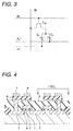
- Fig. 3 is an equivalent circuit diagram of the ferroelectric memory
- Fig. 4 is a sectional view thereof. As seen from these figures.
- the ferroelectric memory is characterized in that it includes a dummy capacitor C D and a memory capacitor C F the first electrodes (storage node electrodes) of which are connected to one of the source and drain of a select transistor T SW and which draw the same hysteresis curve, the second electrodes of these capacitors C D and C F are connected to a first plate line PL + and a second plate line PL - , and the potentials of these plate lines are set so as to polarize the dummy capacitor C D and the memory capacitor C F in opposite directions to each other.
- the ferroelectric memory includes an MOSFET serving as a select transistor consisting of source/drain layers 2 of p-type impurity regions formed on the surface of an n-type Si substrate 1 and a gate electrode formed between the source/drain regions through a gate insulating film 3; and a ferroelectric capacitor consisting of a storage node electrode 5 formed so as to be in contact with one of the source/drain electrodes, a ferroelectric film 6 formed on the storage node electrode 5, and a first and a second plate electrode 7 and 8 formed on the ferroelectric film 6 and having equal areas.
- MOSFET serving as a select transistor consisting of source/drain layers 2 of p-type impurity regions formed on the surface of an n-type Si substrate 1 and a gate electrode formed between the source/drain regions through a gate insulating film 3
- a ferroelectric capacitor consisting of a storage node electrode 5 formed so as to be in contact with one of the source/drain electrodes, a ferroelectric film 6 formed
- the ferroelectric capacitor consists of a dummy capacitor CD formed with the storage node electrode 5 and the first plate electrode 7 and a memory capacitor CF formed with the storage node 5 and the second plate electrode 8. These first and second plate electrodes are connected to the first plate line PL + and the second plate line PL - , respectively and hold their polarization in opposite directions to each other.
- the gate electrode is made of a poly-silicon film and the storage node electrode and plate electrode are made of a two-layer structure of Iridium and Iridium oxide and the ferroelectric layer is made of a PZD layer.
- reference numeral 9 denotes an interlayer insulating film of silicon oxide.
- the ferroelectric film was made of STN and PZT, it may be made of the ferroelectric of e.g. SBT or high permitivity dielectric film of e.g. BST.
- the ferroelectric layer may be formed in a split structure and modified if appropriate.
- a memory capacitor and a dummy capacitor were used for a single select transistor.
- the invention should not be limited to such an arrangement, but can be applied to any other device using a ferroelectric capacitor.
- the invention can be applied the ferroelectric memory in an MFSFET structure in which the gate dielectric film of an MOSFET is formed of a ferroelectric film as a second embodiment.
- Fig. 9 is an equivalent circuit diagram of the ferroelectric memory
- Fig. 10 is a sectional view thereof.
- the ferroelectric memory is characterized in that gate electrode includes a first electrode 14, a second ferroelectric film 17 and a third ferroelectric film 18 which are divided, and the second and the third electrodes are set so as to polarize them in opposite directions to each other.
- the MFSFET structure of ferroelectric memory includes source/drain layers 2 of p-type impurity regions formed on the surface of an n-type Si substrate 1 and a first gate electrode 14 formed between the source/drain regions through a gate insulating film 3 of a first ferroelectric film; a second ferroelectric film 16 formed on the first gate electrode 14; and the second and the third gate electrodes 17,18 formed on the second ferroelectric film 16 having equal areas.
- the second and third electrodes are held at predetermined potentials so that the feroelectric film corresponding to the second and third electrodes to hold their polarization in opposite directions to each other.
- a ferroelectric memory which can cancel the imprint characteristic to have advantages of a long life, good characteristic and great reliability.
- a ferroelectric memory comprising a select transistor and a ferroelectric capacitor is characterized in that the ferroelectric capacitor includes a dummy capacitor and a memory capacitor the first electrodes (storage node electrodes) of which are connected to one of the source and drain of the select transistor and which draw the same hysteresis curve, the second electrodes of the dummy capacitor and the memory capacitor are connected to a first plate line and a second plate line, and the potentials of these plate lines are set so as to polarize the dummy capacitor and the memory capacitor in opposite directions to each other with respect to the first electrode.
Landscapes
- Engineering & Computer Science (AREA)
- Computer Hardware Design (AREA)
- Semiconductor Memories (AREA)
- Dram (AREA)
Applications Claiming Priority (2)
| Application Number | Priority Date | Filing Date | Title |
|---|---|---|---|
| JP27529599A JP3596746B2 (ja) | 1999-09-28 | 1999-09-28 | 強誘電体キャパシタおよびこれを用いた強誘電体メモリ |
| JP27529599 | 1999-09-28 |
Publications (2)
| Publication Number | Publication Date |
|---|---|
| EP1089339A2 true EP1089339A2 (de) | 2001-04-04 |
| EP1089339A3 EP1089339A3 (de) | 2001-10-10 |
Family
ID=17553451
Family Applications (1)
| Application Number | Title | Priority Date | Filing Date |
|---|---|---|---|
| EP00121031A Withdrawn EP1089339A3 (de) | 1999-09-28 | 2000-09-27 | Ferroelektrischer Kondensator und ferroelektrische Speicheranordnung |
Country Status (3)
| Country | Link |
|---|---|
| EP (1) | EP1089339A3 (de) |
| JP (1) | JP3596746B2 (de) |
| KR (1) | KR20010030506A (de) |
Families Citing this family (1)
| Publication number | Priority date | Publication date | Assignee | Title |
|---|---|---|---|---|
| JP3760470B2 (ja) | 2004-01-06 | 2006-03-29 | セイコーエプソン株式会社 | 記憶回路、半導体装置、及び電子機器 |
Family Cites Families (8)
| Publication number | Priority date | Publication date | Assignee | Title |
|---|---|---|---|---|
| US4853893A (en) * | 1987-07-02 | 1989-08-01 | Ramtron Corporation | Data storage device and method of using a ferroelectric capacitance divider |
| JP3169599B2 (ja) * | 1990-08-03 | 2001-05-28 | 株式会社日立製作所 | 半導体装置、その駆動方法、その読み出し方法 |
| JP3098629B2 (ja) * | 1992-09-18 | 2000-10-16 | 株式会社日立製作所 | 強誘電体トランジスタ、それを用いた半導体記憶デバイス、半導体応用機器及び人工知能システム |
| JP3222243B2 (ja) * | 1993-01-25 | 2001-10-22 | 株式会社日立製作所 | 半導体記憶装置とそれを用いた情報処理システム |
| JP3247023B2 (ja) * | 1994-01-13 | 2002-01-15 | ローム株式会社 | 誘電体キャパシタ、不揮発性メモリおよびその製造方法 |
| KR970076816A (ko) * | 1996-05-06 | 1997-12-12 | 김광호 | 누설 전류를 이용한 다진법 강유전체 랜덤 액세서 메모리 |
| EP0837504A3 (de) * | 1996-08-20 | 1999-01-07 | Ramtron International Corporation | Teilweise oder ganz eingekapselte ferroelektrische Anordnung |
| EP1035587A1 (de) * | 1997-08-28 | 2000-09-13 | Rohm Co., Ltd. | Halbleiterbauelement und zugehöriges hertstellungsverfahren |
-
1999
- 1999-09-28 JP JP27529599A patent/JP3596746B2/ja not_active Expired - Lifetime
-
2000
- 2000-09-27 KR KR1020000056691A patent/KR20010030506A/ko not_active Withdrawn
- 2000-09-27 EP EP00121031A patent/EP1089339A3/de not_active Withdrawn
Also Published As
| Publication number | Publication date |
|---|---|
| JP2001101875A (ja) | 2001-04-13 |
| JP3596746B2 (ja) | 2004-12-02 |
| EP1089339A3 (de) | 2001-10-10 |
| KR20010030506A (ko) | 2001-04-16 |
Similar Documents
| Publication | Publication Date | Title |
|---|---|---|
| US6285577B1 (en) | Non-volatile memory using ferroelectric capacitor | |
| US6838718B2 (en) | Ferroelectric capacitor and ferroelectric memory | |
| JP3239109B2 (ja) | 強誘電体不揮発性メモリとその読み出し方法 | |
| US6456520B1 (en) | Semiconductor memory and method for driving the same | |
| JP3377762B2 (ja) | 強誘電体不揮発性メモリ | |
| CN1143316C (zh) | 铁电存储器装置 | |
| KR100332511B1 (ko) | 강유전체 메모리 장치와 그 구동 방법 | |
| US6404667B1 (en) | 2T-1C ferroelectric random access memory and operation method thereof | |
| US20010043484A1 (en) | Nonvolatile memory and its driving method | |
| US5977577A (en) | Ferroelectric based memory devices utilizing low curie point ferroelectrics and encapsulation | |
| US20020141224A1 (en) | Semiconductor memory and method for driving the same | |
| KR100340074B1 (ko) | 넓은 액티브영역 상부에 위치한 강유전체 커패시터를 갖는강유전체 기억소자 | |
| JP3131340B2 (ja) | 強誘電体記憶素子 | |
| EP1089339A2 (de) | Ferroelektrischer Kondensator und ferroelektrische Speicheranordnung | |
| US6901002B2 (en) | Ferroelectric memory | |
| US6753560B2 (en) | Semiconductor memory and method for driving the same | |
| CN1171313C (zh) | 由阻性铁电存储单元组成的存储装置 | |
| JP2002270789A (ja) | 強誘電体メモリ | |
| JP3320474B2 (ja) | 半導体記憶装置 | |
| US6972980B2 (en) | Semiconductor memory devices and methods of fabricating semiconductor memory device | |
| JP3360471B2 (ja) | 強誘電体記憶装置 | |
| US7161202B2 (en) | Semiconductor memory device and method of reading data | |
| JPH05206411A (ja) | 不揮発性記憶素子およびこれを利用した不揮発性記憶装置、ならびに不揮発性記憶装置の駆動方法 | |
| JP3181046B2 (ja) | 不揮発性メモリ | |
| JP2025165647A (ja) | 記憶装置 |
Legal Events
| Date | Code | Title | Description |
|---|---|---|---|
| PUAI | Public reference made under article 153(3) epc to a published international application that has entered the european phase |
Free format text: ORIGINAL CODE: 0009012 |
|
| AK | Designated contracting states |
Kind code of ref document: A2 Designated state(s): AT BE CH CY DE DK ES FI FR GB GR IE IT LI LU MC NL PT SE Kind code of ref document: A2 Designated state(s): DE FR GB |
|
| AX | Request for extension of the european patent |
Free format text: AL;LT;LV;MK;RO;SI |
|
| RIC1 | Information provided on ipc code assigned before grant |
Free format text: 7H 01L 27/108 A, 7G 11C 11/22 B |
|
| PUAL | Search report despatched |
Free format text: ORIGINAL CODE: 0009013 |
|
| AK | Designated contracting states |
Kind code of ref document: A3 Designated state(s): AT BE CH CY DE DK ES FI FR GB GR IE IT LI LU MC NL PT SE |
|
| AX | Request for extension of the european patent |
Free format text: AL;LT;LV;MK;RO;SI |
|
| 17P | Request for examination filed |
Effective date: 20011212 |
|
| AKX | Designation fees paid |
Free format text: DE FR GB |
|
| 17Q | First examination report despatched |
Effective date: 20090422 |
|
| STAA | Information on the status of an ep patent application or granted ep patent |
Free format text: STATUS: THE APPLICATION IS DEEMED TO BE WITHDRAWN |
|
| 18D | Application deemed to be withdrawn |
Effective date: 20090903 |