EP1088347B1 - Single charge carrier transistor and detection method using the same - Google Patents
Single charge carrier transistor and detection method using the same Download PDFInfo
- Publication number
- EP1088347B1 EP1088347B1 EP99957113A EP99957113A EP1088347B1 EP 1088347 B1 EP1088347 B1 EP 1088347B1 EP 99957113 A EP99957113 A EP 99957113A EP 99957113 A EP99957113 A EP 99957113A EP 1088347 B1 EP1088347 B1 EP 1088347B1
- Authority
- EP
- European Patent Office
- Prior art keywords
- transistor
- transistor according
- heterojunction
- semiconductor material
- layer
- Prior art date
- Legal status (The legal status is an assumption and is not a legal conclusion. Google has not performed a legal analysis and makes no representation as to the accuracy of the status listed.)
- Expired - Lifetime
Links
Images


Classifications
-
- B—PERFORMING OPERATIONS; TRANSPORTING
- B82—NANOTECHNOLOGY
- B82Y—SPECIFIC USES OR APPLICATIONS OF NANOSTRUCTURES; MEASUREMENT OR ANALYSIS OF NANOSTRUCTURES; MANUFACTURE OR TREATMENT OF NANOSTRUCTURES
- B82Y10/00—Nanotechnology for information processing, storage or transmission, e.g. quantum computing or single electron logic
-
- H—ELECTRICITY
- H10—SEMICONDUCTOR DEVICES; ELECTRIC SOLID-STATE DEVICES NOT OTHERWISE PROVIDED FOR
- H10D—INORGANIC ELECTRIC SEMICONDUCTOR DEVICES
- H10D30/00—Field-effect transistors [FET]
- H10D30/01—Manufacture or treatment
- H10D30/014—Manufacture or treatment of FETs having zero-dimensional [0D] or one-dimensional [1D] channels, e.g. quantum wire FETs, single-electron transistors [SET] or Coulomb blockade transistors
-
- H—ELECTRICITY
- H10—SEMICONDUCTOR DEVICES; ELECTRIC SOLID-STATE DEVICES NOT OTHERWISE PROVIDED FOR
- H10D—INORGANIC ELECTRIC SEMICONDUCTOR DEVICES
- H10D30/00—Field-effect transistors [FET]
- H10D30/40—FETs having zero-dimensional [0D], one-dimensional [1D] or two-dimensional [2D] charge carrier gas channels
- H10D30/402—Single electron transistors; Coulomb blockade transistors
-
- H—ELECTRICITY
- H10—SEMICONDUCTOR DEVICES; ELECTRIC SOLID-STATE DEVICES NOT OTHERWISE PROVIDED FOR
- H10D—INORGANIC ELECTRIC SEMICONDUCTOR DEVICES
- H10D30/00—Field-effect transistors [FET]
- H10D30/40—FETs having zero-dimensional [0D], one-dimensional [1D] or two-dimensional [2D] charge carrier gas channels
- H10D30/43—FETs having zero-dimensional [0D], one-dimensional [1D] or two-dimensional [2D] charge carrier gas channels having one-dimensional [1D] charge carrier gas channels, e.g. quantum wire FETs or transistors having 1D quantum-confined channels
-
- H—ELECTRICITY
- H10—SEMICONDUCTOR DEVICES; ELECTRIC SOLID-STATE DEVICES NOT OTHERWISE PROVIDED FOR
- H10D—INORGANIC ELECTRIC SEMICONDUCTOR DEVICES
- H10D62/00—Semiconductor bodies, or regions thereof, of devices having potential barriers
- H10D62/80—Semiconductor bodies, or regions thereof, of devices having potential barriers characterised by the materials
- H10D62/81—Semiconductor bodies, or regions thereof, of devices having potential barriers characterised by the materials of structures exhibiting quantum-confinement effects, e.g. single quantum wells; of structures having periodic or quasi-periodic potential variation
- H10D62/812—Single quantum well structures
- H10D62/813—Quantum wire structures
-
- H—ELECTRICITY
- H10—SEMICONDUCTOR DEVICES; ELECTRIC SOLID-STATE DEVICES NOT OTHERWISE PROVIDED FOR
- H10D—INORGANIC ELECTRIC SEMICONDUCTOR DEVICES
- H10D62/00—Semiconductor bodies, or regions thereof, of devices having potential barriers
- H10D62/80—Semiconductor bodies, or regions thereof, of devices having potential barriers characterised by the materials
- H10D62/81—Semiconductor bodies, or regions thereof, of devices having potential barriers characterised by the materials of structures exhibiting quantum-confinement effects, e.g. single quantum wells; of structures having periodic or quasi-periodic potential variation
- H10D62/812—Single quantum well structures
- H10D62/814—Quantum box structures
-
- H—ELECTRICITY
- H10—SEMICONDUCTOR DEVICES; ELECTRIC SOLID-STATE DEVICES NOT OTHERWISE PROVIDED FOR
- H10D—INORGANIC ELECTRIC SEMICONDUCTOR DEVICES
- H10D62/00—Semiconductor bodies, or regions thereof, of devices having potential barriers
- H10D62/80—Semiconductor bodies, or regions thereof, of devices having potential barriers characterised by the materials
- H10D62/85—Semiconductor bodies, or regions thereof, of devices having potential barriers characterised by the materials being Group III-V materials, e.g. GaAs
-
- Y—GENERAL TAGGING OF NEW TECHNOLOGICAL DEVELOPMENTS; GENERAL TAGGING OF CROSS-SECTIONAL TECHNOLOGIES SPANNING OVER SEVERAL SECTIONS OF THE IPC; TECHNICAL SUBJECTS COVERED BY FORMER USPC CROSS-REFERENCE ART COLLECTIONS [XRACs] AND DIGESTS
- Y10—TECHNICAL SUBJECTS COVERED BY FORMER USPC
- Y10S—TECHNICAL SUBJECTS COVERED BY FORMER USPC CROSS-REFERENCE ART COLLECTIONS [XRACs] AND DIGESTS
- Y10S977/00—Nanotechnology
- Y10S977/902—Specified use of nanostructure
- Y10S977/932—Specified use of nanostructure for electronic or optoelectronic application
- Y10S977/936—Specified use of nanostructure for electronic or optoelectronic application in a transistor or 3-terminal device
- Y10S977/937—Single electron transistor
Definitions
- This invention relates to an improved structure for a semiconductor device and a method using said device.
- the carriers are confined to a potential or quantum well.
- a two dimensional electron gas is formed if the carriers are electrons (or a two dimensional hole gas is formed if the majority carriers are holes).
- the potential well is of such a size that it can hold only a few electrons (typically between 0 and 20). Furthermore, once this number is fixed (by an external contact potential) it does not fluctuate in time by more than one electron.
- Such devices are confined to operate at low temperatures (typically less than liquid nitrogen temperatures) due to the physics which allows them to function.
- the devices rely on the fact that the potential well has a small capacitance, and the energy that it takes for electrons to charge this well is quite large. If the device is cooled to low temperatures the electron thermal energy becomes less than the charging energy. Without a significant source-drain voltage bias the electrons cannot travel through the potential well. This is known as Coulomb blockade.
- SET Single Electron Transistors
- the SET is suited for applications where it is necessary to measure small fluctuations of charge without disturbing the system under study, or for providing low power transistor action. They also have potential for sensitive detectors of pressure, acceleration and temperature at least. Other detectors may be envisaged.
- the transistor of the first aspect of the invention may be referred to as a Zener single charge carrier transistor, e.g. a Zener single electron transistor (Zener SET).
- a Zener single electron transistor Zener SET
- Prior art transistors can be referred to as unipolar single electron transistors.
- Zener single charge carrier transistors are advantageous because they are potentially simpler to fabricate and control, they may operate at higher temperatures than prior art devices, both n-type and p-type devices may be fabricated, and confinement may be enhanced due to the low effective mass of conduction electrons in p-type devices.
- single charge carrier transistors are physically small (e.g. nanoscale) when compared to conventional field effect transistors resulting in a higher packaging density though lower power density.
- the first material may be InSb or Cd x Hg 1-x Te.
- the second material may be InAlSb or CdTe or Cd x Hg 1-x Te.
- the heterojunction may be provided as a single layer of first material adjacent to a single layer of second material. Alternatively, the heterojunction may be provided as a single layer of first material between two layers of second material.
- the first material having a band gap of less than 0.5eV may be considered a narrow band gap semiconductor.
- the second material may be considered a wide band gap semiconductor.
- Other materials may be suitable for the first and second materials.
- the value of x may be chosen to tend to one (that is CdTe), CdTe is preferred for its electronic properties but may not be achievable in view of other physical considerations: for example crystal growth considerations and lattice mismatch.
- a third material which may be provided as a layer.
- the third material may function as the first gate electrode.
- the third material may be a metal. It may be Al or Au, or may be any other suitable conductor. Such a structure is advantageous because the presence of the gate electrode allows the electron / hole gas to be controlled within the heterojunction.
- the second gate electrode may be fabricated from a metal. Such a structure in combination with the first gate electrode allows the electron / hole gas to be controlled.
- the second gate electrode may be insulated from the materials forming the heterojunction by at least a single layer of insulation.
- An insulation layer is advantageous in that it modifies the interaction between the second gate electrode and the heterojunction in such a way as to give the desired functionality.
- At least one (and preferably two) side gate may be provided. These may help to control the electron / hole gas in the desired manner.
- the side gates may be insulated from the materials forming the heterojunction by a layer of insulation.
- the side gate may comprise an elongate area along one side of the first or second material above the heterojunction.
- each forms an area along a side of the first or second material which sides are opposite each other.
- the areas may be rectangles.
- the two side gates are in the same plane and there exists a gap within that plane between the two areas of side gates.
- the side gates preferably extend generally parallel to each other.
- the second gate electrode is provided above and may be insulated from the side gate. Again such a structure allows the electron/ hole gas to be controlled in the desired manner.
- the insulation may be silicon dioxide SiO 2 or any other suitable insulation material. Indeed, different types of insulation material may be used for different layers of insulation. Or indeed, the layers of insulation separating the materials of the heterojunction and the side gate may be the same as the layers of insulation separating the side gate from the second gate electrode.
- the second gate electrode comprises a primary portion which extends over the gap between the side gates.
- Such a structure may have a large influence in the electrons in the electron / hole gas.
- the second gate electrode may have a first broad region connected to a second broad region via a narrower waist region.
- the second gate electrode may be a bow tie shape possibly with the central, waist, portion of the bow tie extending over the gap between the side gates.
- the effect of the side gate electrodes may be thought of as creating a quantum wire wherein electrons or holes are held by an applied electric field in a narrow strip within the electron sheet.
- the use of electrodes to form the quantum wire may be thought of as soft confinement.
- An alternative, or additional, way of forming the quantum wire may be with hard confinement as opposed to through the provision of side gates (soft confinement).
- the heterojunction may be provided between a strip of first material and a layer of second material. That is the width of the first material may be much less than the width of the second material. This potentially provides a hard confined quantum wire.
- the first and second materials may be as described in relation to the embodiments hereinbefore. In particular the first material may be thought of as a narrow band gap semiconductor and the second material may be thought of as a wide band gap semiconductor.
- the strip of narrow band gap semiconductor may have a width of substantially 50nm. However, the strip may have a width substantially in the range 10nm to 90nm. More preferably the width of the strip may be substantially in the range 25nm to 75nm.
- a second gate electrode may be provided overlying the strip of narrow band gap semiconductor.
- the second gate electrode may or may not overlie regions of the wide band gap semiconductor where no narrow band gap semiconductor is present.
- the second gate electrode has the bow tie structure discussed hereinbefore.
- the second gate electrode is separated from the semiconductor materials by a layer of insulator which may be silicon dioxide.
- the narrower waist region of the second gate electrode may have a width of substantially 50nm. However, the narrower waist region may have a width substantially in the range 10nm to 90nm. More preferably the width of the narrower waist region may be substantially in the range 25nm to 75nm. The skilled person will appreciate that this may form a region where the second gate electrode overlies the narrow band gap semiconductor which is substantially square having a side of substantially 50nm.
- the quantum wire may be provided by the V-Groove method for fabricating quantum wires. This may be preferred over the method of providing a thin strip of narrow band gap semiconductor because the confinement offered may be cleaner.
- the transistor may contain a V shaped notch or groove within a substrate layer.
- a layer of second material may be provided lining the groove.
- the layer of second material may also form a V shaped notch or groove.
- a region of first material may be provided in the V of the notch in the second material.
- the notch may be substantially filled with a layer of insulation. However, the notch may be partially filled with insulation such that the first material is covered. The insulation may cover the region of first material.
- a second gate electrode is provided on top of the layer of insulation.
- the second gate electrode has a bow tie shape having a primary portion as described hereinbefore. The primary portion of the second gate electrode may overlie the region of first material.
- a plurality of quantum wires may be provided in a single groove. The wires may be stacked one above the other.
- the transistor may have a layer of second material having a non planar surface upon which a quantum wire has been fabricated.
- the substrate may have a surface which is stepped (i.e. has a plurality of steps) due to being cut off-axis. That is off-axis to a material lattice plane having atoms aligned to form a smooth surface.
- the angle of a plane of the stepped surface of the substrate may be adapted to provide a specified distance between steps. The distance may be in the range 0.1 ⁇ m to 1 ⁇ m. The skilled person will realise the more acute the angle the longer the distance between the steps.
- Regions of first material may be provided in regions associated with the steps in the second material.
- the regions of the first material may be covered with an insulator.
- the insulator may also cover the surface of the second material where there is no first material provided. It will be appreciated by the skilled person that when fabricating quantum wires by such a method the thin layer of the first material may cover the entire non planar surface of the second material with regions being concentrated in regions associated with the steps.
- a second gate electrode may be provided on top of the layer of insulation overlying the regions of first material.
- the gate may have substantially the dimensions as discussed hereinbefore.
- the second gate electrode may overlie a number of regions of first material.
- the regions of first material may be considered to be quantum wires.
- the transistor may comprise at least one ridge grown quantum wire.
- the ridge grown quantum wire may include reverse mesa etched from a substrate. Ridges in-between the reverse mesa may have a layer of second material provided upon a surface. On a surface region of the layer of second material there may be provided a region of first material.
- a second gate electrode may be provided overlying the region of first material and the second gate electrode may be separated from the first material be a layer of insulation.
- the transistor may be thought of as providing a controllable single potential maxima or minima along a quantum wire. That is providing a quantum dot within a quantum wire.
- a drain and a source electrode At a third and fourth end of the transistor (which are at opposite ends of a plane parallel with the first and second sides) there may be provided a drain and a source electrode.
- the drain and source electrodes allow a bias voltage to be applied to the electron/ hole gas to cause the carriers to flow through the transistor.
- the dimensions of the primary portion of the second gate electrode are such that it is less than substantially 100nm in width measured along an axis perpendicular to the drain and the source. More preferably less than 75nm and most preferably less than substantially 50nm.
- the transistor may be fabricated so that the primary charge carriers may be either holes or electrons. That is the device may be fabricated so that it is p-type or n-type. This has the advantage that circuits could potentially be fabricated from a number of transistors according to the invention such that the device would use complementary technology similar to the philosophy behind CMOS technology. As the skilled person will realise this is advantageous in that such devices are low power because they have substantially zero quiescent current.
- the primary portion of the second gate electrode may cause a single potential barrier when a bias voltage is applied between the first and second gates. (Conversely if the primary charge carriers are holes a single potential well may be caused when a voltage is applied between the first and second gate).
- Narrow band gap may be defined as a material having a valence band at an appropriate level to complement the conduction band such that electrons can use the valence band to tunnel in the manner described hereinbefore.
- An alternative or additional definition of narrow band gap may be the use of a material having a band gap of less than 1 ⁇ 2 eV between the conduction and valence bands.
- the layers may be arranged such that a permanent strain is caused throughout the layer of first material. This is advantageous because it may shift the energy of heavy holes within the valence band such that electrons tunnelling through the transistor can only utilise light holes. As a result of this it is likely that the performance of an n-type device will be as good as the p-type device due to the low effective mass of the light holes.
- the present invention facilitates a method of holding a charge carrier within a quantum dot created by a pair of gate electrodes across a heterojunction, in which a bias voltage applied across the gate electrodes cause a single potential barrier or well within a sheet of charge near the heterojunction such that one or more charge carriers are confined within the barrier or well.
- the method comprises using narrow band gap semiconductors to provide the sheet of charge. These may show the necessary physical properties to allow the single maxima or minima of field to be provided, in which a charge carrier can be held within.
- a potential barrier would be caused in an n-type device and a potential well would be caused in a p-type device.
- the method may comprise cooling the heterojunction, for example to substantially liquid nitrogen temperatures (77K).
- the method may comprise cooling the heterojunction to below liquid nitrogen temperatures, perhaps to substantially liquid helium temperatures (4K). As discussed in the introduction such cooling may bring the thermal energy of the charge carriers below the charging energy of the quantum dot.
- the method may comprise applying a bias along the heterojunction (between a source and drain electrode) such that charge carriers are caused to flow along the heterojunction when potential caused by the gate electrodes allows.
- An advantage of such a method is that the effect may be used directly to measure small changes in an electric field (perhaps this can be thought of as a sensitive electrometer).
- the change of current caused is on an order substantially equal to the original current flowing through the transistor.
- a Zener SET may be enough to alter the physical dimensions of the potential barrier or well. This may change the energy of a quantised level in the valence band relative to the Fermi energy (the energy levels are a function of geometry as well as a function of applied bias voltage) thus causing a change in the current flow through the device.
- the method may have a sensitivity comparable with that of a scanning electron microscope.
- the single electron transistor relies on Zener Tunnelling of electrons into the valence band of the semi-conductor material from which it is fabricated, to provide transistor action.
- the energy levels of heavy holes within the valence band are shifted below the energy levels of light holes.
- the energy level of the energy levels of heavy holes are shifted by applying a permanent strain to a material in which electron confinement occurs.
- the material in which the electron confinement occurs is a narrow band gap semiconductor, which may be provided between two layers of wide band gap semiconductor.
- the strain may be applied to the narrow band gap semiconductor by lattice strain caused by interaction with the wide band gap semiconductor.
- Figures 1 and 2 show the prior art wherein a single electron transistor (or unipolar SET) is provided from a heterojunction of typical III-V semiconductor such as GaAs.
- a device 1 having a layer of GaAs 2 adjacent a layer of Al x Ga 1-x As 4 to form a heterojunction.
- a first gate electrode 6 is provided at a bottom region of the device and a pair of second gate electrodes 8 are provided at a top portion of the device opposite the heterojunction from the first gate electrode 6.
- Each of the second gate electrodes 8 comprises an elongate member with two stubs 10, 12 symmetrically arranged about a central axis of the elongate member projecting toward the centre of the device.
- Electrons can be confined in a direction perpendicular to an axis passing through both of the gate electrodes in a thin sheet in the GaAs 2 just above the Al x Ga 1-x As 4 close to the heterojunction interface.
- a potential energy profile of this sheet is shown in Figure 2 .
- Figure 2a shows an energy level diagram for Figure 2 .
- the conduction band 13 and the valence band 15 are shown. Peaks 17, 19 in these bands are caused by the field from the gate electrodes 10, 12.
- the region 14 of Figure 2 is shown to be between the two peaks in the conduction band 13.
- the skilled person will appreciate that the valence band 15 is not important in the unipolar SET because of the large band gap (it is so far removed when looking at the energies that it plays no role in the functioning of the device).
- the region 14 of minimal potential is referred to as a quantum dot and the confinement is said to be soft since it is controlled by the voltage on the gate electrodes. Conversely, confinement out of the thin sheet is said to be hard since it is due to the heterojunction step itself.
- the source-drain resistance in a direction perpendicular to an axis passing between the gate electrodes
- the source-drain resistance will essentially be infinite provided the source-drain voltage difference is small (that is V SD ⁇ ⁇ e/C where C is the effective capacitance of the dot).
- FIG. 4 An approximation of a device 19 according to the present invention is shown in Figure 4 . This simplified structure makes it clear just how the device operates and the structure has been used to explain the concept.
- a layer of InAlSb (wide band gap second material) 20 is provided in association with a layer of InSb 22 forming a heterojunction wherein carriers are hard confined in a thin sheet in the InSb 22 (narrow band gap first material) just above the InAlSb 20 close to the heterojunction interface.
- a so called two dimensional electron (or hole) gas is formed near to the heterojunction.
- a first gate 24 electrode is positioned at a first side of the heterojunction and a second gate electrode 26 comprising a pair of electrodes is positioned at the opposite side of the heterojunction.
- Each one of the second gate electrodes 26 comprises an elongated metallic electrode.
- a drain 28 and a source 30 electrode are positioned at either end of layers of InSb 22 and InAlSb 20 (along a plane running parallel to the heterojunction).
- a third gate electrode 34 which in this case is circular (but in other embodiments could be of a different shape, such as a cube or rectangle) is positioned between the second gate electrodes 26.
- the size of the third electrode 34 and spacing from the second gate electrodes 26 is critical to the operation of the device.
- the geometry of the electrodes 26, 34 effect the potential field in the two-dimensional electron gas near to the heterojunction interface, as does the field applied to the gate electrodes.
- a potential applied to the first, second and third gate electrodes 24, 26, 34 causes a potential energy field as shown in Figure 5 .
- the position of the drain 28 and the source 30 electrodes are shown at either end of Figure 5 to show the orientation of the Figure relative to the device shown in Figure 4 ).
- the graph shows the potential along a two dimensional plane in the InSb close to the heterojunction.
- the z-axis of the graph represents the potential at each point on the plane.
- the second and third electrodes 26, 34 In, operation, (for an n-type device) the second and third electrodes 26, 34 would be biased negatively relative to the first electrode 24. Furthermore, the bias on the third electrode 34 would be most negative. [Conversely, for a p-type device on the second and third electrodes 26, 34 would be biased positively relative to the first electrode 24, with the third electrode 34 being most positive].
- Figure 5 the field due to the potential applied between the first and second electrodes 24, 26 causes a gulley 35.
- the field due to the potential applied between the first and third electrodes 24, 34 causes the potential barrier 37.
- Figure 5 is for an n-type device. Similarly a p-type device would have a central potential well.
- V SD A potential is also applied between the drain 28 and source 30 electrodes (V SD ).
- V SD causes a slight bias on electrons within the transistor causing them to tend to move towards the drain 28 electrode.
- an electron When an electron is within the potential barrier 37 it may Zener tunnel out of the barrier 37 either toward the source 30 or drain 28 electrodes. Without V SD being applied there would be an equal chance of either direction occurring.
- V SD increases the probability of electrons tunnelling out of the barrier 37 in the direction of the drain 28 electrode.
- V SD is necessarily small and has a maximum magnitude of substantially kT (approximately 25meV at room temperature). Should V SD have too large a magnitude electrons will pass through the potential barrier 37 without being held inside.
- the device 19 makes use of the narrow band gap of less than 0.5eV which exists in materials such as InSb and Cd x Hg 1-x Te. That is the energy level of the valence band is relatively close to the energy level of the conduction band when compared to other III-V semiconductor such as GaAs and InAs.
- a material used for this embodiment has a narrow band gap. That is, the valence band is at an appropriate level to complement the conduction band so that electrons can use the valence band to tunnel.
- the conduction and valence bands of the InSb move. If a high enough bias voltage is applied to the gate electrode 34 the energy of the valence band edge below this gate can be higher than the conduction band edge at a point along the gulley 35.
- Zener tunnelling we refer to this device as a Zener single-electron transistor (Zener SET).
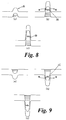
- Figure 8c shows that if a further bias voltage (is made more negative) is applied to the gate electrode 34 then the energy level 38 moves above the Fermi energy and electrons can no longer tunnel across the heterojunction. Therefore, the device of Figures 4 , 6, and 7 operates in a manner similar to that of the device of Figure 1 and current flows as is shown in Figure 3 . There is a large gap between the unoccupied level in the dot and the next (unoccupied) level, representing both the quantisation gap of the single-electron states, due to confinement and the Coulomb blockade energy (energy of repulsion between two charge carriers in the dot). Note, however, that for the conventional SET the gate bias is increased whereas for the Zener SET it is decreased.
- Electrons only have a single effective mass and this is equal to the mass of a light hole.
- the electrons it is desirable for the electrons to occupy light hole states due to the larger energy gap between these hole states meaning that the transistor is less influenced by changes in temperature. As the temperature increases so does the probability that an electron in the gulley 35 region be thermally excited above the Fermi energy. Should the electrons energy become coincident with that of the hole state conduction will occur. Since the light holes have a larger energy separation more temperature change is likely to be needed to equate the energy of the hole state to the energy of the thermally excited electron in the gulley 35.
- the wide band gap structure has a small lattice spacing.
- the narrow band gap structure By growing the narrow band gap structure thin enough in association with the wide band gap material it is possible to ensure the lattice matching causes a permanent compression throughout the narrow layer. This ensures only the light holes are utilised for tunnelling. That is, the lattice of the narrow band gap material must match the lattice of the wide band gap material at the interface; because the wide gap has the smaller spacing the narrow gap material will be strained by the matching of the lattices.
- Figure 9 shows a similar energy level diagram to Figure 8 but for a device fabricated from p-type material wherein the majority charge carriers are holes. In this situation if a sufficiently large positive bias is applied to the gate electrode 34 the conduction band edge below this gate electrode may become lower than the Fermi energy.
- Such a p-type SET has the advantage over the unstrained n-type SET of enhanced quantisation in the confined region due to the lower effective mass of the conduction-band electrons.
- a quantum dot such as occurs in the confined region of a SET, behaves in some ways like an atom showing, for example, electron affinity, and ionisation in the Coulomb blockade regime, where at low-temperatures the quantum dot will have an integral number of charge carriers. It has been suggested that a quantum dot may be referred to as an 'artificial atom'. (Dots occupied with one, two, three ... electrons being artificial H, He, Li respectively). Two artificial atoms in series will be the analogue of molecules. For the Zener set such a molecule may be fabricated by creating two barriers as was done for the single SET in GaAs. A typical conduction band edge profile would be similar to that for the single SET in GaAs but the device would behave quite differently due to the presence or resonant levels in both the valence bands (barrier regions) and conduction band (well region).
- the tunnelling barriers into and out of the quantum dot must have high resistance (> > the resistance quantum ⁇ 13kQ) in order to have strong confinement. If this were not the case then the resonant bound state would be broadened, the Coulomb blockade reduced and the device would always be switched on. This need not be the case for the Zener SET.
- the single barrier is sufficiently strong the device will be essentially 'off' at the appropriate gate bias since the tunnelling of conduction electrons will be small ( Figure 9a ).
- the Zener tunnelling barriers need not be strong in order for the transistor to switch on.
- Zener barriers may be 'tuned' by choice of semi-conductor and geometry.
- the current through the device will be relatively large, significant 'co-tunnelling' will take place and the fluctuations in electron number on the quantum dot may well exceed unity. This will also cause the ⁇ turn on' to be more gradual and will reduce the Coulomb blockade, resulting in weaker SET oscillations.
- this mode may be preferable for some applications where a low 'on' resistance is required.
- the turn-on will be sharp and the subsequent SET oscillations sharp, as with the unipolar device.
- FIG. 4 The device shown in Figure 4 is of a simplified nature so that the principles of operation can be more easily explained. However, a more realistic device structure is shown in Figures 6 and 7 .
- a heterojunction is formed by a 20nm thick layer of InAlSb (wide band gap second material) 100 provided in association with a 20nm thick layer of InSb (narrow band gap first material) 102.
- the sheet of electrons are maintained by the heterojunction in a thin layer in the InSb layer near to the junction. This is to prevent tunnelling of electrons from the second and third gates into the InSb.
- a source electrode 106 and a drain electrode 108 are provided at each end of the heterojunction on top of the InSb 102 layer. Between the source 106 and the drain 108 there is provided a layer of insulation 104, in this case SiO 2 , on top of the InSb 102 layer.
- a side gate electrode 110, 112 fabricated from a third material.
- the layer of SiO 2 insulates the side gate electrodes 110, 112 from the InSb layer 102.
- a fillet of SiO 2 insulation 114, 116 which insulate a second gate electrode 118, in the shape of a bow tie, from the side gate electrodes 110, 112.
- the electrodes are fabricated from gold on top of a layer of chromium.
- the chromium ensures the gold adheres to the transistor.
- the choice of materials for the electrodes is not critical.
- the two side gates 110, 112 are rectangular in plan and occupy a region at each side of the transistor.
- the two rectangular areas do not meet in the central region 120 of the transistor and thus the central region 120 is not covered by the side gates 110, 112.
- the middle portion (primary portion of the second gate electrode) 122 of the bow tie shaped second gate electrode 118 is arranged to be over the central region 120 of the transistor.
- This central region of the gate transmits a much larger voltage to the InSb than elsewhere since it is not screened by the SiO 2 fillet. This can be most clearly seen in Figure 7 .
- a first gate electrode 124 At an underneath of the transistor, as viewed in Figure 7 , there is provided a first gate electrode 124.
- first and second gate electrodes 124, 118 allows electrons to tunnel into the quantum central confined region, when an energy level in either the valence or conduction band (depending on whether p-type or n-type) equals the Fermi energy.
- a voltage between the drain and the source electrodes causes a current to flow when conditions in the central region near the heterojunction are such that electrons can tunnel across.
- the side gate electrodes 110, 112 allow the potential at the edge potions of the heterojunction to be held sufficiently high (at regions 150, 152 in Figure 5 ) so as to ensure that electrons cannot be transmitted through this portion, but not too high, otherwise electrons could Zener tunnel from the central region, out of the gulley toward electrodes 150, 152.
- the potential applied to the side gate electrodes 110, 112 will be optimised to ensure that electrons are held within the gulley 35; a compromise value ensuring electrons can not bypass the potential maxima 37, nor tunnel out of the gulley 35 towards regions 150, 152.
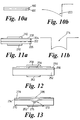
- the heterojunction can be formed by a variety of different methods, which are represented in Figures 10 and 11 .
- the structure of Figure 10a has been described with a layer of InSb (narrow band gap semi-conductor) 102, adjacent a layer of InAlSb (wide band gap semi-conductor) 100.
- This structure provides the potential profile shown in Figure 10b . Electrons are held at the minimum of potential (shown at 200). However, should the potential profile be too shallow the confinement of the electrons within the thin sheet of charge near the heterojunction will not be strong and electrons can easily escape out of the plane of charge.
- Figure 10a is a simplification of the earlier Figures and oxide layers and gates would be provided in addition to the layers 100, 102.
- Figure 11a shows an alternative structure for the heterojunction wherein a layer 202 of InSb (narrow band gap semi-conductor) has been provided between two layers of InAlSb (wide band gap semiconductor) 204, 206.
- the layer of InSb 202 is narrower than the layers of InAlSb 204, 206 to achieve the necessary potential conditions throughout the InSb to maintain electrons and also to achieve lattice mismatch as described hereinbefore thus imparting a permanent strain on the InSb layer.
- the layer 202 have significant thickness then two heterojunctions would be provided in series. However, the thickness of the InSb layer 102 cannot be too small because it becomes hard to fabricate and also the charge capacity (i.e. the number of electrons that the layer 102 can physically hold) becomes too small. In this embodiment the preferred thickness is 20nm.
- Figure 11a also shows an oxide layer 208 that has been grown on top of the InAlSb layer 204. This oxide layer 208 may be necessary to remove material mismatch problems between a top gate electrode 210 and the InAlSb layer 204. A bottom gate electrode 212 is also shown.
- Figure 11b shows the potential profile for the heterojunction formed by the structure of Figure 11a . Rather than relying on the minimum of potential to hold electrons in the region 200 there is now a defined well 214 in which electrons are held. It does not matter whether or not the potential profile is too shallow; electrons will still be maintained within the thin sheet of charge in the vicinity of the heterojunction.
- Figure 11a may be preferred over the structure of Figure 10a in view of a cleaner junction interface at the top junction resulting in a higher carrier mobility.
- a two dimensional electron sheet could also be provided by the use of modulation doping in a layer of wide band gap semionductor adjacent a layer of narrow band gap semiconductor as will be appreciated by the skilled person.
- the devices of Figures 4 and 6 rely on soft confinement (the provision of electric fields) to maintain electrons within the electron sheet provided by the heterojunction in a narrow strip or quantum wire. As the skilled person will appreciate hard confinement wherein the electrons are controlled by physical barriers to form a quantum wire is also possible. Such structures are shown in Figures 12 to 16 .
- Figure 12 shows a first possibility wherein a layer of second material, or wide band gap semionductor 250 is provided on top of a substrate 252 which would generally be an n + material.
- a narrow strip of narrow band gap semiconductor 254, or first material is provided on top of the wide band gap material. Generally this would be provided by depositing a layer of narrow band gap material onto the wide band gap material and then etching the narrow band gap material to the desired width.
- Both the narrow band gap strip 254 and the wide band gap layer 250 are covered in a layer of insulator 256, in this case silicon dioxide.
- a second gate electrode 258 is provided which as can be seen in Figure 14 is a bow tie shape having a primary portion 260, approximately 50nm in width, which extends over the strip of narrow band gap material 254 (shown in outline).
- a first electrode 262 is provided on the underside of the substrate 252. Also seen in Figure 14 are third and fourth electrodes 261,263 which form drain and source electrodes.
- the device of Figure 12 would operate in the same manner as those of Figures 4 and 6 except that are no side gates to which a potential must be applied.
- the electrons / holes are maintained in a strip due to the structure of the device.
- the quantum dot is provided within the strip of charge carriers by a potential applied between the first 262 and the second 258 gate electrodes.
- Figure 13 shows a further structure for a transistor according to the invention which, as with the device of Figure 12 , relies on hard confinement to provide a quantum wire.
- a substrate 270 is provided in which there is a V shaped groove 272.
- a layer of wide band gap semiconductor 274 or second material is provided on top of the substrate which covers the surface of the groove 272.
- the V of the groove in the substrate 270 will not be perfectly sharp but will be rounded.
- the layer of the wide band gap material 274 will also have a rounded V, as can be seen in Figure 17 .
- Figure 17 shows an enlargement of the groove 272 of Figure 13 where a substrate 270 is shown with the groove 272 fabricated therein.
- the groove has a rounded V portion.
- a layer 274 of second material has been deposited on the substrate 270
- the lattice planes of second material at the edge portion of the V are ⁇ 111 > compared to ⁇ 001 > planes at surface regions outside the groove 272.
- the first material grows faster on the ⁇ 001 > planes during deposition and therefore a thin coating of first material 276 can be provided which is concentrated in the base of the groove 272.
- the groove is then filled with an insulator 278. The process can be repeated so a number of wires are provided vertically above one another.
- a layer of insulation 278 is provided which fills the groove and covers the layer of wide band gap material.
- the narrow bad gap semiconductor is preferentially deposited in the V of the groove, a thin layer of narrow band gap semiconductor is likely to be present on the sides of the groove and will thus be sandwiched between the wide band gap semiconductor 274 and the insulator 278.
- a second gate electrode 280 On top of the layer of insulation there is provided a second gate electrode 280.
- a first gate electrode 282 is provided underneath the substrate 270.
- Figure 13 is also shown in plan in Figure 14 , wherein the second electrode 280 can be seen to have the bow tie structure with a primary portion 260 overlying the groove (shown in outline) and consequently the region of first material.
- the device of Figure 13 will operate in the same manner as the device of Figure 12 .
- FIG. 15 Yet a further alternative structure for providing a transistor according to the invention is shown in Figure 15 .
- a wafer of intrinsic wide band gap semi conductor 290 is provided. This wafer has been cut at an angle (possibly at up to substantially 6°) to a plane wherein the atoms in the lattice are aligned. This provides a stepped surface as can be seen in the Figure.
- a layer of insulator 296 is provided which covers the narrow band gap semiconductor and a second electrode 298 is provided on top of the insulator. Again a first electrode 300 is provided underneath the structure.
- the device of Figure 15 functions in a similar manner to the device described in relation to Figures 12 and 13 .
- Figure 16 shows a further alternative structure for fabricating the transistor relying on hard confinement of electrons.
- a substrate 302 is etched with reverse mesa stripes 304 providing a plurality of ridges 306. The etching is such that sharp regions 308 are provided at end portions of the ridges 306.
- the lattice structure is such that when further layers are deposited onto the ridges the deposition process is much more rapid on the side walls than at the sharp region 308.
- a wide band gap material is deposited on to the ridge 306 forming a layer 310.
- a layer of narrow band gap material 312 is deposited on to the wide band gap material 310.
- the narrow band gap material is deposited the differential deposition rates are exploited so that primarily only a region of narrow band gap material exists at the top most region of the ridge 306.
- the structure is subsequently covered in an insulating layer 314. The insulation may completely fill the reverse mesa.
- Gate electrodes are provided in the same manner as in Figures 12, 13 , 15 and the device operates in a similar manner.
Landscapes
- Engineering & Computer Science (AREA)
- Chemical & Material Sciences (AREA)
- Nanotechnology (AREA)
- Physics & Mathematics (AREA)
- Mathematical Physics (AREA)
- Theoretical Computer Science (AREA)
- Crystallography & Structural Chemistry (AREA)
- Junction Field-Effect Transistors (AREA)
- Insulated Gate Type Field-Effect Transistor (AREA)
- Thin Film Transistor (AREA)
Applications Claiming Priority (3)
| Application Number | Priority Date | Filing Date | Title |
|---|---|---|---|
| GB9813142A GB2338592A (en) | 1998-06-19 | 1998-06-19 | Single electron transistor |
| GB9813142 | 1998-06-19 | ||
| PCT/GB1999/001885 WO1999066561A1 (en) | 1998-06-19 | 1999-06-18 | Single charge carrier transistor, method of holding a charge carrier within a quantum dot, and method of detection |
Publications (2)
| Publication Number | Publication Date |
|---|---|
| EP1088347A1 EP1088347A1 (en) | 2001-04-04 |
| EP1088347B1 true EP1088347B1 (en) | 2011-11-23 |
Family
ID=10833967
Family Applications (2)
| Application Number | Title | Priority Date | Filing Date |
|---|---|---|---|
| EP99957113A Expired - Lifetime EP1088347B1 (en) | 1998-06-19 | 1999-06-18 | Single charge carrier transistor and detection method using the same |
| EP99928062A Withdrawn EP1088346A1 (en) | 1998-06-19 | 1999-06-18 | Quantum wire field-effect transistor and method of making the same |
Family Applications After (1)
| Application Number | Title | Priority Date | Filing Date |
|---|---|---|---|
| EP99928062A Withdrawn EP1088346A1 (en) | 1998-06-19 | 1999-06-18 | Quantum wire field-effect transistor and method of making the same |
Country Status (5)
| Country | Link |
|---|---|
| US (2) | US6498354B1 (https=) |
| EP (2) | EP1088347B1 (https=) |
| JP (2) | JP2002518851A (https=) |
| GB (1) | GB2338592A (https=) |
| WO (2) | WO1999066561A1 (https=) |
Families Citing this family (29)
| Publication number | Priority date | Publication date | Assignee | Title |
|---|---|---|---|---|
| WO2003005450A2 (en) * | 2001-05-18 | 2003-01-16 | President And Fellows Of Harvard College | Nanoscale wires and related devices |
| US6683337B2 (en) * | 2001-02-09 | 2004-01-27 | Micron Technology, Inc. | Dynamic memory based on single electron storage |
| US6978070B1 (en) * | 2001-08-14 | 2005-12-20 | The Programmable Matter Corporation | Fiber incorporating quantum dots as programmable dopants |
| JP4334246B2 (ja) | 2003-02-27 | 2009-09-30 | 富士通株式会社 | 量子半導体装置及びその製造方法 |
| JP4304338B2 (ja) * | 2004-01-13 | 2009-07-29 | 独立行政法人産業技術総合研究所 | 光検出素子 |
| CN101065845A (zh) * | 2004-06-04 | 2007-10-31 | 可编程物公司 | 包含作为可编程掺杂剂的量子点的层状复合薄膜 |
| US7465595B2 (en) | 2004-11-09 | 2008-12-16 | Fujitsu Limited | Quantum device, manufacturing method of the same and controlling method of the same |
| JP5202312B2 (ja) * | 2005-07-06 | 2013-06-05 | インターナショナル レクティフィアー コーポレイション | 第iii族窒化物エンハンスメント型デバイス |
| US7358581B2 (en) * | 2005-11-17 | 2008-04-15 | Kulite Semiconductor Products, Inc. | Quantum dot based pressure switch |
| WO2007120983A1 (en) * | 2006-02-17 | 2007-10-25 | Ravenbrick, Llc | Quantum dot switching device |
| US7601946B2 (en) * | 2006-09-12 | 2009-10-13 | Ravenbrick, Llc | Electromagnetic sensor incorporating quantum confinement structures |
| DK2106560T3 (en) | 2007-01-24 | 2017-08-07 | Ravenbrick Llc | THERMAL REPLACED OPTICAL DOWN CONVERTER FILTER |
| US8363307B2 (en) * | 2007-02-28 | 2013-01-29 | Ravenbrick, Llc | Multicolor light emitting device incorporating tunable quantum confinement devices |
| US7936500B2 (en) * | 2007-03-02 | 2011-05-03 | Ravenbrick Llc | Wavelength-specific optical switch |
| AU2008274933B2 (en) | 2007-07-11 | 2012-03-08 | Ravenbrick, Llc | Thermally switched reflective optical shutter |
| JP5568013B2 (ja) | 2007-09-19 | 2014-08-06 | レイブンブリック,エルエルシー | ナノスケールのワイヤグリッドを組み込んだ窓用低放射膜 |
| US8169685B2 (en) | 2007-12-20 | 2012-05-01 | Ravenbrick, Llc | Thermally switched absorptive window shutter |
| JP5671449B2 (ja) | 2008-04-23 | 2015-02-18 | レイブンブリック,エルエルシー | 反射性表面およびサーモリフレクティブ表面についてのグレアを調整する方法および装置 |
| US9116302B2 (en) | 2008-06-19 | 2015-08-25 | Ravenbrick Llc | Optical metapolarizer device |
| WO2010022294A2 (en) | 2008-08-20 | 2010-02-25 | Ravenbrick, Llc | Methods for fabricating thermochromic filters |
| CN102460238A (zh) | 2009-04-10 | 2012-05-16 | 雷文布里克有限责任公司 | 结合有宾主型结构的热切换滤光器 |
| US8947760B2 (en) | 2009-04-23 | 2015-02-03 | Ravenbrick Llc | Thermotropic optical shutter incorporating coatable polarizers |
| WO2011053853A2 (en) * | 2009-10-30 | 2011-05-05 | Ravenbrick Llc | Thermochromic filters and stopband filters for use with same |
| WO2011062708A2 (en) | 2009-11-17 | 2011-05-26 | Ravenbrick Llc | Thermally switched optical filter incorporating a refractive optical structure |
| JP5890390B2 (ja) | 2010-03-29 | 2016-03-22 | レイブンブリック,エルエルシー | ポリマ安定化型サーモトロピック液晶デバイス |
| GB2480265B (en) * | 2010-05-10 | 2013-10-02 | Toshiba Res Europ Ltd | A semiconductor device and a method of fabricating a semiconductor device |
| EP2576934A4 (en) | 2010-06-01 | 2014-01-01 | Ravenbrick Llc | MULTIFUNCTIONAL CONSTRUCTION PART |
| US8933488B2 (en) * | 2010-12-03 | 2015-01-13 | The Board Of Trustees Of The Leland Stanford Junior Univerity | Heterostructure field effect transistor with same channel and barrier configuration for PMOS and NMOS |
| US9859409B2 (en) * | 2016-04-28 | 2018-01-02 | International Business Machines Corporation | Single-electron transistor with wrap-around gate |
Family Cites Families (16)
| Publication number | Priority date | Publication date | Assignee | Title |
|---|---|---|---|---|
| CA1315865C (en) | 1988-02-09 | 1993-04-06 | Elyahou Kapon | Semiconductor super lattice heterostructure fabrication methods, structures and devices |
| US5497015A (en) | 1988-11-12 | 1996-03-05 | Sony Corporation | Quantum interference transistor |
| EP0386388A1 (en) | 1989-03-10 | 1990-09-12 | International Business Machines Corporation | Method for the epitaxial growth of a semiconductor structure |
| EP0661733A2 (en) * | 1993-12-21 | 1995-07-05 | International Business Machines Corporation | One dimensional silicon quantum wire devices and the method of manufacture thereof |
| GB2288274A (en) * | 1994-03-31 | 1995-10-11 | Sharp Kk | Quantum device and method of making such a device |
| JPH07326730A (ja) | 1994-05-31 | 1995-12-12 | Mitsubishi Electric Corp | 半導体装置,その製造方法,単一電子デバイス,及びその製造方法 |
| JP3256091B2 (ja) * | 1994-08-23 | 2002-02-12 | 株式会社日立製作所 | 結晶粒の形成方法および半導体装置 |
| US5654558A (en) * | 1994-11-14 | 1997-08-05 | The United States Of America As Represented By The Secretary Of The Navy | Interband lateral resonant tunneling transistor |
| GB2295272B (en) | 1994-11-15 | 1998-01-14 | Toshiba Cambridge Res Center | Semiconductor device |
| JP3837674B2 (ja) * | 1995-03-20 | 2006-10-25 | 富士通株式会社 | 量子半導体装置 |
| DE19522351A1 (de) * | 1995-06-20 | 1997-01-09 | Max Planck Gesellschaft | Verfahren zur Herstellung von Quantenstrukturen, insbesondere von Quantenpunkten und Tunnelbarrieren sowie Bauelemente mit solchen Quantenstrukturen |
| JPH1093109A (ja) * | 1996-09-13 | 1998-04-10 | Nippon Telegr & Teleph Corp <Ntt> | クーロンブロッケイド素子とその製造方法 |
| US5945686A (en) * | 1997-04-28 | 1999-08-31 | Hitachi, Ltd. | Tunneling electronic device |
| KR100240629B1 (ko) * | 1997-08-30 | 2000-01-15 | 정선종 | 테라급 집적이 가능한 대전효과 트랜지스터 및 그 제조방법 |
| KR19990024760A (ko) * | 1997-09-08 | 1999-04-06 | 정선종 | 양자세선 제조 방법 |
| US6063688A (en) * | 1997-09-29 | 2000-05-16 | Intel Corporation | Fabrication of deep submicron structures and quantum wire transistors using hard-mask transistor width definition |
-
1998
- 1998-06-19 GB GB9813142A patent/GB2338592A/en not_active Withdrawn
-
1999
- 1999-06-18 JP JP2000555300A patent/JP2002518851A/ja not_active Abandoned
- 1999-06-18 WO PCT/GB1999/001885 patent/WO1999066561A1/en not_active Ceased
- 1999-06-18 JP JP2000555299A patent/JP4864202B2/ja not_active Expired - Fee Related
- 1999-06-18 EP EP99957113A patent/EP1088347B1/en not_active Expired - Lifetime
- 1999-06-18 WO PCT/GB1999/001940 patent/WO1999066562A1/en not_active Ceased
- 1999-06-18 EP EP99928062A patent/EP1088346A1/en not_active Withdrawn
- 1999-06-18 US US09/719,484 patent/US6498354B1/en not_active Expired - Fee Related
- 1999-06-18 US US09/701,884 patent/US6753593B1/en not_active Expired - Lifetime
Also Published As
| Publication number | Publication date |
|---|---|
| JP2002518851A (ja) | 2002-06-25 |
| EP1088347A1 (en) | 2001-04-04 |
| JP2002518850A (ja) | 2002-06-25 |
| US6753593B1 (en) | 2004-06-22 |
| WO1999066562A1 (en) | 1999-12-23 |
| EP1088346A1 (en) | 2001-04-04 |
| WO1999066561A1 (en) | 1999-12-23 |
| GB9813142D0 (en) | 1998-08-19 |
| GB2338592A (en) | 1999-12-22 |
| JP4864202B2 (ja) | 2012-02-01 |
| US6498354B1 (en) | 2002-12-24 |
Similar Documents
| Publication | Publication Date | Title |
|---|---|---|
| EP1088347B1 (en) | Single charge carrier transistor and detection method using the same | |
| US4575924A (en) | Process for fabricating quantum-well devices utilizing etch and refill techniques | |
| US5701016A (en) | Semiconductor device and method for its manufacture | |
| US4581621A (en) | Quantum device output switch | |
| US5923046A (en) | Quantum dot memory cell | |
| EP0177374B1 (en) | High-speed semiconductor device | |
| JP3745015B2 (ja) | 電子デバイス | |
| US4912531A (en) | Three-terminal quantum device | |
| US4721983A (en) | Three terminal tunneling device | |
| US4704622A (en) | Negative transconductance device | |
| JPS6327065A (ja) | ヘテロ接合二重チャネル半導体装置、この半導体装置を応用した電界効果トランジスタ、ならびにこの半導体装置を応用した負のコンダクタンスをもつ装置 | |
| JP2781021B2 (ja) | 磁界センサ | |
| US5932889A (en) | Semiconductor device with floating quantum box | |
| US5032877A (en) | Quantum-coupled ROM | |
| US4783427A (en) | Process for fabricating quantum-well devices | |
| US5986291A (en) | Field effect devices | |
| US4799091A (en) | Quantum device output switch | |
| CA2442127C (en) | Negative-resistance field-effect element | |
| Wu et al. | Negative differential conductance observed in a lateral double constriction device | |
| US4645707A (en) | Semiconductor devices | |
| JPS639388B2 (https=) | ||
| US4969018A (en) | Quantum-well logic using self-generated potentials | |
| EP0545255B1 (en) | Quantum semiconductor device employing quantum boxes for enabling compact size and high-speed operation | |
| EP0170044B1 (en) | Quantum-coupled device | |
| GB2270590A (en) | Semiconductor devices including field effect transistors |
Legal Events
| Date | Code | Title | Description |
|---|---|---|---|
| PUAI | Public reference made under article 153(3) epc to a published international application that has entered the european phase |
Free format text: ORIGINAL CODE: 0009012 |
|
| 17P | Request for examination filed |
Effective date: 20001202 |
|
| AK | Designated contracting states |
Kind code of ref document: A1 Designated state(s): DE FR GB |
|
| RAP1 | Party data changed (applicant data changed or rights of an application transferred) |
Owner name: QINETIQ LIMITED |
|
| 17Q | First examination report despatched |
Effective date: 20080204 |
|
| RAP1 | Party data changed (applicant data changed or rights of an application transferred) |
Owner name: QINETIQ LIMITED |
|
| GRAP | Despatch of communication of intention to grant a patent |
Free format text: ORIGINAL CODE: EPIDOSNIGR1 |
|
| RTI1 | Title (correction) |
Free format text: SINGLE CHARGE CARRIER TRANSISTOR AND DETECTION METHOD USING THE SAME |
|
| GRAS | Grant fee paid |
Free format text: ORIGINAL CODE: EPIDOSNIGR3 |
|
| GRAA | (expected) grant |
Free format text: ORIGINAL CODE: 0009210 |
|
| AK | Designated contracting states |
Kind code of ref document: B1 Designated state(s): DE FR GB |
|
| REG | Reference to a national code |
Ref country code: GB Ref legal event code: FG4D |
|
| REG | Reference to a national code |
Ref country code: DE Ref legal event code: R096 Ref document number: 69943880 Country of ref document: DE Effective date: 20120202 |
|
| PLBE | No opposition filed within time limit |
Free format text: ORIGINAL CODE: 0009261 |
|
| STAA | Information on the status of an ep patent application or granted ep patent |
Free format text: STATUS: NO OPPOSITION FILED WITHIN TIME LIMIT |
|
| 26N | No opposition filed |
Effective date: 20120824 |
|
| REG | Reference to a national code |
Ref country code: DE Ref legal event code: R097 Ref document number: 69943880 Country of ref document: DE Effective date: 20120824 |
|
| GBPC | Gb: european patent ceased through non-payment of renewal fee |
Effective date: 20120618 |
|
| REG | Reference to a national code |
Ref country code: FR Ref legal event code: ST Effective date: 20130228 |
|
| REG | Reference to a national code |
Ref country code: DE Ref legal event code: R119 Ref document number: 69943880 Country of ref document: DE Effective date: 20130101 |
|
| PG25 | Lapsed in a contracting state [announced via postgrant information from national office to epo] |
Ref country code: DE Free format text: LAPSE BECAUSE OF NON-PAYMENT OF DUE FEES Effective date: 20130101 Ref country code: GB Free format text: LAPSE BECAUSE OF NON-PAYMENT OF DUE FEES Effective date: 20120618 Ref country code: FR Free format text: LAPSE BECAUSE OF NON-PAYMENT OF DUE FEES Effective date: 20120702 |