EP1088347B1 - Single charge carrier transistor and detection method using the same - Google Patents
Single charge carrier transistor and detection method using the same Download PDFInfo
- Publication number
- EP1088347B1 EP1088347B1 EP99957113A EP99957113A EP1088347B1 EP 1088347 B1 EP1088347 B1 EP 1088347B1 EP 99957113 A EP99957113 A EP 99957113A EP 99957113 A EP99957113 A EP 99957113A EP 1088347 B1 EP1088347 B1 EP 1088347B1
- Authority
- EP
- European Patent Office
- Prior art keywords
- transistor
- transistor according
- heterojunction
- semiconductor material
- layer
- Prior art date
- Legal status (The legal status is an assumption and is not a legal conclusion. Google has not performed a legal analysis and makes no representation as to the accuracy of the status listed.)
- Expired - Lifetime
Links
- 239000002800 charge carrier Substances 0.000 title claims description 22
- 238000001514 detection method Methods 0.000 title claims description 3
- 239000004065 semiconductor Substances 0.000 claims abstract description 69
- 229910004613 CdTe Inorganic materials 0.000 claims abstract description 5
- 230000005669 field effect Effects 0.000 claims abstract description 5
- 239000000463 material Substances 0.000 claims description 127
- 239000010410 layer Substances 0.000 claims description 89
- 238000009413 insulation Methods 0.000 claims description 19
- 238000000034 method Methods 0.000 claims description 17
- 239000000758 substrate Substances 0.000 claims description 15
- 238000005036 potential barrier Methods 0.000 claims description 11
- 239000002356 single layer Substances 0.000 claims description 8
- 230000008859 change Effects 0.000 claims description 7
- 239000013078 crystal Substances 0.000 claims description 2
- 230000005641 tunneling Effects 0.000 claims 3
- WPYVAWXEWQSOGY-UHFFFAOYSA-N indium antimonide Chemical compound [Sb]#[In] WPYVAWXEWQSOGY-UHFFFAOYSA-N 0.000 abstract description 22
- 230000004888 barrier function Effects 0.000 description 18
- VYPSYNLAJGMNEJ-UHFFFAOYSA-N Silicium dioxide Chemical compound O=[Si]=O VYPSYNLAJGMNEJ-UHFFFAOYSA-N 0.000 description 16
- 239000002096 quantum dot Substances 0.000 description 14
- 239000000969 carrier Substances 0.000 description 8
- 238000010586 diagram Methods 0.000 description 8
- 239000012212 insulator Substances 0.000 description 8
- 238000005381 potential energy Methods 0.000 description 8
- 239000000377 silicon dioxide Substances 0.000 description 8
- 229910001218 Gallium arsenide Inorganic materials 0.000 description 7
- 239000004047 hole gas Substances 0.000 description 7
- IJGRMHOSHXDMSA-UHFFFAOYSA-N Atomic nitrogen Chemical compound N#N IJGRMHOSHXDMSA-UHFFFAOYSA-N 0.000 description 6
- 230000008901 benefit Effects 0.000 description 6
- 229910052681 coesite Inorganic materials 0.000 description 5
- 229910052906 cristobalite Inorganic materials 0.000 description 5
- 229910052682 stishovite Inorganic materials 0.000 description 5
- 229910052905 tridymite Inorganic materials 0.000 description 5
- 238000000151 deposition Methods 0.000 description 4
- 230000000694 effects Effects 0.000 description 4
- 239000007788 liquid Substances 0.000 description 4
- 238000000926 separation method Methods 0.000 description 4
- 230000000295 complement effect Effects 0.000 description 3
- 238000001816 cooling Methods 0.000 description 3
- 230000008021 deposition Effects 0.000 description 3
- 230000005684 electric field Effects 0.000 description 3
- 239000010931 gold Substances 0.000 description 3
- 229910052737 gold Inorganic materials 0.000 description 3
- 229910052757 nitrogen Inorganic materials 0.000 description 3
- 230000010355 oscillation Effects 0.000 description 3
- 235000012239 silicon dioxide Nutrition 0.000 description 3
- VYZAMTAEIAYCRO-UHFFFAOYSA-N Chromium Chemical compound [Cr] VYZAMTAEIAYCRO-UHFFFAOYSA-N 0.000 description 2
- 230000009471 action Effects 0.000 description 2
- 229910052804 chromium Inorganic materials 0.000 description 2
- 239000011651 chromium Substances 0.000 description 2
- 239000002772 conduction electron Substances 0.000 description 2
- 238000005516 engineering process Methods 0.000 description 2
- 238000005530 etching Methods 0.000 description 2
- PCHJSUWPFVWCPO-UHFFFAOYSA-N gold Chemical compound [Au] PCHJSUWPFVWCPO-UHFFFAOYSA-N 0.000 description 2
- 229910052734 helium Inorganic materials 0.000 description 2
- 239000012774 insulation material Substances 0.000 description 2
- 230000003993 interaction Effects 0.000 description 2
- 229910052751 metal Inorganic materials 0.000 description 2
- 239000002184 metal Substances 0.000 description 2
- 230000008569 process Effects 0.000 description 2
- 230000035945 sensitivity Effects 0.000 description 2
- 239000007787 solid Substances 0.000 description 2
- 230000005533 two-dimensional electron gas Effects 0.000 description 2
- 229910000673 Indium arsenide Inorganic materials 0.000 description 1
- 230000001133 acceleration Effects 0.000 description 1
- 230000001154 acute effect Effects 0.000 description 1
- 238000005513 bias potential Methods 0.000 description 1
- 230000015572 biosynthetic process Effects 0.000 description 1
- 238000012512 characterization method Methods 0.000 description 1
- 239000011248 coating agent Substances 0.000 description 1
- 238000000576 coating method Methods 0.000 description 1
- 150000001875 compounds Chemical class 0.000 description 1
- 230000006835 compression Effects 0.000 description 1
- 238000007906 compression Methods 0.000 description 1
- 239000004020 conductor Substances 0.000 description 1
- 230000003247 decreasing effect Effects 0.000 description 1
- 230000001419 dependent effect Effects 0.000 description 1
- 238000005137 deposition process Methods 0.000 description 1
- 239000007789 gas Substances 0.000 description 1
- 239000001307 helium Substances 0.000 description 1
- SWQJXJOGLNCZEY-UHFFFAOYSA-N helium atom Chemical compound [He] SWQJXJOGLNCZEY-UHFFFAOYSA-N 0.000 description 1
- RPQDHPTXJYYUPQ-UHFFFAOYSA-N indium arsenide Chemical compound [In]#[As] RPQDHPTXJYYUPQ-UHFFFAOYSA-N 0.000 description 1
- 239000002674 ointment Substances 0.000 description 1
- 230000003287 optical effect Effects 0.000 description 1
- 238000004806 packaging method and process Methods 0.000 description 1
- 230000000704 physical effect Effects 0.000 description 1
- 239000013589 supplement Substances 0.000 description 1
- 230000005428 wave function Effects 0.000 description 1
Images


Classifications
-
- B—PERFORMING OPERATIONS; TRANSPORTING
- B82—NANOTECHNOLOGY
- B82Y—SPECIFIC USES OR APPLICATIONS OF NANOSTRUCTURES; MEASUREMENT OR ANALYSIS OF NANOSTRUCTURES; MANUFACTURE OR TREATMENT OF NANOSTRUCTURES
- B82Y10/00—Nanotechnology for information processing, storage or transmission, e.g. quantum computing or single electron logic
-
- H—ELECTRICITY
- H01—ELECTRIC ELEMENTS
- H01L—SEMICONDUCTOR DEVICES NOT COVERED BY CLASS H10
- H01L29/00—Semiconductor devices adapted for rectifying, amplifying, oscillating or switching, or capacitors or resistors with at least one potential-jump barrier or surface barrier, e.g. PN junction depletion layer or carrier concentration layer; Details of semiconductor bodies or of electrodes thereof ; Multistep manufacturing processes therefor
- H01L29/02—Semiconductor bodies ; Multistep manufacturing processes therefor
- H01L29/12—Semiconductor bodies ; Multistep manufacturing processes therefor characterised by the materials of which they are formed
- H01L29/122—Single quantum well structures
- H01L29/125—Quantum wire structures
-
- H—ELECTRICITY
- H01—ELECTRIC ELEMENTS
- H01L—SEMICONDUCTOR DEVICES NOT COVERED BY CLASS H10
- H01L29/00—Semiconductor devices adapted for rectifying, amplifying, oscillating or switching, or capacitors or resistors with at least one potential-jump barrier or surface barrier, e.g. PN junction depletion layer or carrier concentration layer; Details of semiconductor bodies or of electrodes thereof ; Multistep manufacturing processes therefor
- H01L29/02—Semiconductor bodies ; Multistep manufacturing processes therefor
- H01L29/12—Semiconductor bodies ; Multistep manufacturing processes therefor characterised by the materials of which they are formed
- H01L29/122—Single quantum well structures
- H01L29/127—Quantum box structures
-
- H—ELECTRICITY
- H01—ELECTRIC ELEMENTS
- H01L—SEMICONDUCTOR DEVICES NOT COVERED BY CLASS H10
- H01L29/00—Semiconductor devices adapted for rectifying, amplifying, oscillating or switching, or capacitors or resistors with at least one potential-jump barrier or surface barrier, e.g. PN junction depletion layer or carrier concentration layer; Details of semiconductor bodies or of electrodes thereof ; Multistep manufacturing processes therefor
- H01L29/66—Types of semiconductor device ; Multistep manufacturing processes therefor
- H01L29/66007—Multistep manufacturing processes
- H01L29/66075—Multistep manufacturing processes of devices having semiconductor bodies comprising group 14 or group 13/15 materials
- H01L29/66227—Multistep manufacturing processes of devices having semiconductor bodies comprising group 14 or group 13/15 materials the devices being controllable only by the electric current supplied or the electric potential applied, to an electrode which does not carry the current to be rectified, amplified or switched, e.g. three-terminal devices
- H01L29/66409—Unipolar field-effect transistors
- H01L29/66446—Unipolar field-effect transistors with an active layer made of a group 13/15 material, e.g. group 13/15 velocity modulation transistor [VMT], group 13/15 negative resistance FET [NERFET]
- H01L29/66469—Unipolar field-effect transistors with an active layer made of a group 13/15 material, e.g. group 13/15 velocity modulation transistor [VMT], group 13/15 negative resistance FET [NERFET] with one- or zero-dimensional channel, e.g. quantum wire field-effect transistors, in-plane gate transistors [IPG], single electron transistors [SET], Coulomb blockade transistors, striped channel transistors
-
- H—ELECTRICITY
- H01—ELECTRIC ELEMENTS
- H01L—SEMICONDUCTOR DEVICES NOT COVERED BY CLASS H10
- H01L29/00—Semiconductor devices adapted for rectifying, amplifying, oscillating or switching, or capacitors or resistors with at least one potential-jump barrier or surface barrier, e.g. PN junction depletion layer or carrier concentration layer; Details of semiconductor bodies or of electrodes thereof ; Multistep manufacturing processes therefor
- H01L29/66—Types of semiconductor device ; Multistep manufacturing processes therefor
- H01L29/68—Types of semiconductor device ; Multistep manufacturing processes therefor controllable by only the electric current supplied, or only the electric potential applied, to an electrode which does not carry the current to be rectified, amplified or switched
- H01L29/76—Unipolar devices, e.g. field effect transistors
- H01L29/7613—Single electron transistors; Coulomb blockade devices
-
- H—ELECTRICITY
- H01—ELECTRIC ELEMENTS
- H01L—SEMICONDUCTOR DEVICES NOT COVERED BY CLASS H10
- H01L29/00—Semiconductor devices adapted for rectifying, amplifying, oscillating or switching, or capacitors or resistors with at least one potential-jump barrier or surface barrier, e.g. PN junction depletion layer or carrier concentration layer; Details of semiconductor bodies or of electrodes thereof ; Multistep manufacturing processes therefor
- H01L29/66—Types of semiconductor device ; Multistep manufacturing processes therefor
- H01L29/68—Types of semiconductor device ; Multistep manufacturing processes therefor controllable by only the electric current supplied, or only the electric potential applied, to an electrode which does not carry the current to be rectified, amplified or switched
- H01L29/76—Unipolar devices, e.g. field effect transistors
- H01L29/772—Field effect transistors
- H01L29/775—Field effect transistors with one dimensional charge carrier gas channel, e.g. quantum wire FET
-
- Y—GENERAL TAGGING OF NEW TECHNOLOGICAL DEVELOPMENTS; GENERAL TAGGING OF CROSS-SECTIONAL TECHNOLOGIES SPANNING OVER SEVERAL SECTIONS OF THE IPC; TECHNICAL SUBJECTS COVERED BY FORMER USPC CROSS-REFERENCE ART COLLECTIONS [XRACs] AND DIGESTS
- Y10—TECHNICAL SUBJECTS COVERED BY FORMER USPC
- Y10S—TECHNICAL SUBJECTS COVERED BY FORMER USPC CROSS-REFERENCE ART COLLECTIONS [XRACs] AND DIGESTS
- Y10S977/00—Nanotechnology
- Y10S977/902—Specified use of nanostructure
- Y10S977/932—Specified use of nanostructure for electronic or optoelectronic application
- Y10S977/936—Specified use of nanostructure for electronic or optoelectronic application in a transistor or 3-terminal device
- Y10S977/937—Single electron transistor
Abstract
Description
- This invention relates to an improved structure for a semiconductor device and a method using said device.
- Over the last two decades there has been much interest in semiconductor devices which operate by restricting the motion of current carriers in one or more directions. In such devices the carriers can only occupy a discrete set of energy levels or sub-bands in one or more dimensions. The motion of the carriers is said to be quantised in the direction of confinement.
- Examples of such known devices are described in the following references: Okada et al.: 1997 Nano Physics and Electronics International Workshop (NPE), Tokyo, JP, 18-20 September 1997, & Solid Sate Electronics, vol. 42, no. 7-8, pages 1419-1423, July-August 1998; C.S. Dürr et al.: Eighth International Conference On Modulated Semiconductor Structures (MSS 8), Santa Barbara, US, 14-18 July 1997, & Physics E, vol. 2, no 1-4, pages 23-27, 15 July 1998;
US-A-5,654,558 ; U. Meirav et al.: Physical Review Letters, vol. 65, no. 6, 6 August 1990, pages 771-774; Y. Wang et al.: Applied Physics Letters, vol. 63, no. 16, 18 October 1993, pages 2257-2259; X.L. Wang et al.: Applied Physics Letters, vol. 66, no. 12, 20 March 1995, pages 1506 - 1508; T. Fukui et al.: Japanese Journal of Applied Physics, Supplements (Extended Abstracts of the 22nd Conference on Solid State Devices and Materials, Sendai, JP), January 1990, pages 753-756. - In heterojunctions, formed by the joining together of two semiconductor compounds of different band gaps, the carriers are confined to a potential or quantum well. A two dimensional electron gas is formed if the carriers are electrons (or a two dimensional hole gas is formed if the majority carriers are holes).
- One particular type of semiconductor device which has been fabricated, typically from GaAs, is the single electron transistor which was invented in 1987. In this device the potential well is of such a size that it can hold only a few electrons (typically between 0 and 20). Furthermore, once this number is fixed (by an external contact potential) it does not fluctuate in time by more than one electron.
- Such devices are confined to operate at low temperatures (typically less than liquid nitrogen temperatures) due to the physics which allows them to function. The devices rely on the fact that the potential well has a small capacitance, and the energy that it takes for electrons to charge this well is quite large. If the device is cooled to low temperatures the electron thermal energy becomes less than the charging energy. Without a significant source-drain voltage bias the electrons cannot travel through the potential well. This is known as Coulomb blockade.
- According to a first aspect of the invention there is provided a field effect single charge carrier transistor as set out in claim 1. Specific embodiments are disclosed in dependent claims 2-20.
- Single Electron Transistors (SET) have the highest charge sensitivity of any man-made device. The SET is suited for applications where it is necessary to measure small fluctuations of charge without disturbing the system under study, or for providing low power transistor action. They also have potential for sensitive detectors of pressure, acceleration and temperature at least. Other detectors may be envisaged.
- The transistor of the first aspect of the invention may be referred to as a Zener single charge carrier transistor, e.g. a Zener single electron transistor (Zener SET). Prior art transistors can be referred to as unipolar single electron transistors.
- Zener single charge carrier transistors are advantageous because they are potentially simpler to fabricate and control, they may operate at higher temperatures than prior art devices, both n-type and p-type devices may be fabricated, and confinement may be enhanced due to the low effective mass of conduction electrons in p-type devices.
- Further advantages of single charge carrier transistors are that they are physically small (e.g. nanoscale) when compared to conventional field effect transistors resulting in a higher packaging density though lower power density.
- The first material may be InSb or CdxHg1-xTe.
- The second material may be InAlSb or CdTe or CdxHg1-xTe. The heterojunction may be provided as a single layer of first material adjacent to a single layer of second material. Alternatively, the heterojunction may be provided as a single layer of first material between two layers of second material.
- The first material having a band gap of less than 0.5eV may be considered a narrow band gap semiconductor. The second material may be considered a wide band gap semiconductor. Other materials may be suitable for the first and second materials.
- The skilled person will realise that should the first material be CdxHg1-xTe the band gap can be tailored to any desired value of less than 0.5eV by adjusting the value of x. As x tends to =0.15 the band gap of the material tends to zero. However, x may be chosen to be an optimal value.
- Should the second material be CdxHg1-xTe the value of x may be chosen to tend to one (that is CdTe), CdTe is preferred for its electronic properties but may not be achievable in view of other physical considerations: for example crystal growth considerations and lattice mismatch.
- There may be provided on a first side of the heterojunction a third material which may be provided as a layer. The third material may function as the first gate electrode. The third material may be a metal. It may be Al or Au, or may be any other suitable conductor. Such a structure is advantageous because the presence of the gate electrode allows the electron / hole gas to be controlled within the heterojunction.
- The second gate electrode may be fabricated from a metal. Such a structure in combination with the first gate electrode allows the electron / hole gas to be controlled.
- The second gate electrode may be insulated from the materials forming the heterojunction by at least a single layer of insulation. An insulation layer is advantageous in that it modifies the interaction between the second gate electrode and the heterojunction in such a way as to give the desired functionality.
- At least one (and preferably two) side gate may be provided. These may help to control the electron / hole gas in the desired manner.
- The side gates may be insulated from the materials forming the heterojunction by a layer of insulation.
- The side gate may comprise an elongate area along one side of the first or second material above the heterojunction. Preferably when two side gates are provided each forms an area along a side of the first or second material which sides are opposite each other. The areas may be rectangles. Most preferably the two side gates are in the same plane and there exists a gap within that plane between the two areas of side gates.
- The side gates preferably extend generally parallel to each other.
- Preferably, the second gate electrode is provided above and may be insulated from the side gate. Again such a structure allows the electron/ hole gas to be controlled in the desired manner.
- The insulation may be silicon dioxide SiO2 or any other suitable insulation material. Indeed, different types of insulation material may be used for different layers of insulation. Or indeed, the layers of insulation separating the materials of the heterojunction and the side gate may be the same as the layers of insulation separating the side gate from the second gate electrode.
- Preferably the second gate electrode comprises a primary portion which extends over the gap between the side gates. Such a structure may have a large influence in the electrons in the electron / hole gas.
- The second gate electrode may have a first broad region connected to a second broad region via a narrower waist region. The second gate electrode may be a bow tie shape possibly with the central, waist, portion of the bow tie extending over the gap between the side gates.
- The skilled person will appreciate that the effect of the side gate electrodes may be thought of as creating a quantum wire wherein electrons or holes are held by an applied electric field in a narrow strip within the electron sheet. The use of electrodes to form the quantum wire may be thought of as soft confinement.
- An alternative, or additional, way of forming the quantum wire may be with hard confinement as opposed to through the provision of side gates (soft confinement).
- In one embodiment the heterojunction may be provided between a strip of first material and a layer of second material. That is the width of the first material may be much less than the width of the second material. This potentially provides a hard confined quantum wire. The first and second materials may be as described in relation to the embodiments hereinbefore. In particular the first material may be thought of as a narrow band gap semiconductor and the second material may be thought of as a wide band gap semiconductor.
- The strip of narrow band gap semiconductor may have a width of substantially 50nm. However, the strip may have a width substantially in the range 10nm to 90nm. More preferably the width of the strip may be substantially in the range 25nm to 75nm.
- In this embodiment a second gate electrode may be provided overlying the strip of narrow band gap semiconductor. The second gate electrode may or may not overlie regions of the wide band gap semiconductor where no narrow band gap semiconductor is present. Preferably the second gate electrode has the bow tie structure discussed hereinbefore.
- Preferably the second gate electrode is separated from the semiconductor materials by a layer of insulator which may be silicon dioxide.
- The narrower waist region of the second gate electrode may have a width of substantially 50nm. However, the narrower waist region may have a width substantially in the range 10nm to 90nm. More preferably the width of the narrower waist region may be substantially in the range 25nm to 75nm. The skilled person will appreciate that this may form a region where the second gate electrode overlies the narrow band gap semiconductor which is substantially square having a side of substantially 50nm.
- In an alternative embodiment the quantum wire may be provided by the V-Groove method for fabricating quantum wires. This may be preferred over the method of providing a thin strip of narrow band gap semiconductor because the confinement offered may be cleaner.
- The transistor may contain a V shaped notch or groove within a substrate layer.
- A layer of second material may be provided lining the groove. The layer of second material may also form a V shaped notch or groove. A region of first material may be provided in the V of the notch in the second material.
- The notch may be substantially filled with a layer of insulation. However, the notch may be partially filled with insulation such that the first material is covered. The insulation may cover the region of first material. Preferably a second gate electrode is provided on top of the layer of insulation. Preferably the second gate electrode has a bow tie shape having a primary portion as described hereinbefore. The primary portion of the second gate electrode may overlie the region of first material. A plurality of quantum wires may be provided in a single groove. The wires may be stacked one above the other.
- In yet another embodiment the transistor may have a layer of second material having a non planar surface upon which a quantum wire has been fabricated.
- The substrate may have a surface which is stepped (i.e. has a plurality of steps) due to being cut off-axis. That is off-axis to a material lattice plane having atoms aligned to form a smooth surface. The angle of a plane of the stepped surface of the substrate may be adapted to provide a specified distance between steps. The distance may be in the range 0.1µm to 1µm. The skilled person will realise the more acute the angle the longer the distance between the steps.
- Regions of first material may be provided in regions associated with the steps in the second material. The regions of the first material may be covered with an insulator. The insulator may also cover the surface of the second material where there is no first material provided. It will be appreciated by the skilled person that when fabricating quantum wires by such a method the thin layer of the first material may cover the entire non planar surface of the second material with regions being concentrated in regions associated with the steps.
- A second gate electrode may be provided on top of the layer of insulation overlying the regions of first material. The gate may have substantially the dimensions as discussed hereinbefore.
- The second gate electrode may overlie a number of regions of first material. The regions of first material may be considered to be quantum wires.
- In yet another embodiment the transistor may comprise at least one ridge grown quantum wire. The ridge grown quantum wire may include reverse mesa etched from a substrate. Ridges in-between the reverse mesa may have a layer of second material provided upon a surface. On a surface region of the layer of second material there may be provided a region of first material.
- A second gate electrode may be provided overlying the region of first material and the second gate electrode may be separated from the first material be a layer of insulation.
- The transistor may be thought of as providing a controllable single potential maxima or minima along a quantum wire. That is providing a quantum dot within a quantum wire.
- The various techniques for forming quantum wires are disclosed in the PhD thesis of Matthew John Steer, dated October 1997, entitled "Optical and Structural Characterisation of III-V Semiconductor Quantum Wires and Quantum Dot Structures" from the University of Sheffield.
- At a third and fourth end of the transistor (which are at opposite ends of a plane parallel with the first and second sides) there may be provided a drain and a source electrode. The drain and source electrodes allow a bias voltage to be applied to the electron/ hole gas to cause the carriers to flow through the transistor.
- Preferably the dimensions of the primary portion of the second gate electrode are such that it is less than substantially 100nm in width measured along an axis perpendicular to the drain and the source. More preferably less than 75nm and most preferably less than substantially 50nm.
- The transistor may be fabricated so that the primary charge carriers may be either holes or electrons. That is the device may be fabricated so that it is p-type or n-type. This has the advantage that circuits could potentially be fabricated from a number of transistors according to the invention such that the device would use complementary technology similar to the philosophy behind CMOS technology. As the skilled person will realise this is advantageous in that such devices are low power because they have substantially zero quiescent current.
- Should the device be fabricated from p-type samples there is the advantage that there is enhanced quantisation in the confined region.
- In use, should the primary charge carriers be electrons, the primary portion of the second gate electrode may cause a single potential barrier when a bias voltage is applied between the first and second gates. (Conversely if the primary charge carriers are holes a single potential well may be caused when a voltage is applied between the first and second gate).
- It may be possible to cause an equivalent potential barrier or well within a non-narrow band gap semi-conductor by applying high gate bias potentials. However, the gradient of the potential field would be such that electrons could not be held within the field; any electron within the well or barrier would be able to Zener tunnel out of the region. That is, the wave function would leak out of the well or barrier, due to the steepness of the sides.
- With a sufficiently high gate (first gate to second gate) bias voltage unoccupied quantised energy levels will occur in the valence band below the primary portion of the second gate electrode. These energy levels may be occupied by charge carriers tunnelling from the conduction band to the valence band (Zener tunnelling).
- Narrow band gap may be defined as a material having a valence band at an appropriate level to complement the conduction band such that electrons can use the valence band to tunnel in the manner described hereinbefore. An alternative or additional definition of narrow band gap may be the use of a material having a band gap of less than ½ eV between the conduction and valence bands.
- Should the heterojunction be provided as a layer of first material between two layers of second material, the layers may be arranged such that a permanent strain is caused throughout the layer of first material. This is advantageous because it may shift the energy of heavy holes within the valence band such that electrons tunnelling through the transistor can only utilise light holes. As a result of this it is likely that the performance of an n-type device will be as good as the p-type device due to the low effective mass of the light holes.
- The present invention facilitates a method of holding a charge carrier within a quantum dot created by a pair of gate electrodes across a heterojunction, in which a bias voltage applied across the gate electrodes cause a single potential barrier or well within a sheet of charge near the heterojunction such that one or more charge carriers are confined within the barrier or well.
- The method comprises using narrow band gap semiconductors to provide the sheet of charge. These may show the necessary physical properties to allow the single maxima or minima of field to be provided, in which a charge carrier can be held within.
- A potential barrier would be caused in an n-type device and a potential well would be caused in a p-type device.
- The method may comprise cooling the heterojunction, for example to substantially liquid nitrogen temperatures (77K). The method may comprise cooling the heterojunction to below liquid nitrogen temperatures, perhaps to substantially liquid helium temperatures (4K). As discussed in the introduction such cooling may bring the thermal energy of the charge carriers below the charging energy of the quantum dot.
- The method may comprise applying a bias along the heterojunction (between a source and drain electrode) such that charge carriers are caused to flow along the heterojunction when potential caused by the gate electrodes allows.
- According to a second aspect of the invention there is provided a method of detection as set out in claim 21.
- An advantage of such a method is that the effect may be used directly to measure small changes in an electric field (perhaps this can be thought of as a sensitive electrometer).
- Preferably the change of current caused is on an order substantially equal to the original current flowing through the transistor.
- Further possible applications may be the formation of an accelerometer or may be of a pressure sensor. The forces exerted on a Zener SET may be enough to alter the physical dimensions of the potential barrier or well. This may change the energy of a quantised level in the valence band relative to the Fermi energy (the energy levels are a function of geometry as well as a function of applied bias voltage) thus causing a change in the current flow through the device.
- The method may have a sensitivity comparable with that of a scanning electron microscope.
- The single electron transistor relies on Zener Tunnelling of electrons into the valence band of the semi-conductor material from which it is fabricated, to provide transistor action.
- Preferably, the energy levels of heavy holes within the valence band are shifted below the energy levels of light holes.
- This has the advantage that only light holes are used as electrons tunnel into the valence band so that it is likely the performance of an n-type device will be as good as the p-type device due to the low effective mass of the light holes.
- Preferably the energy level of the energy levels of heavy holes are shifted by applying a permanent strain to a material in which electron confinement occurs.
- The material in which the electron confinement occurs is a narrow band gap semiconductor, which may be provided between two layers of wide band gap semiconductor.
- The strain may be applied to the narrow band gap semiconductor by lattice strain caused by interaction with the wide band gap semiconductor.
- There now follows by way of example only a detailed description of the present invention with reference to the accompanying drawings of which:
-
Figure 1 shows a single electron transistor according to the prior art; -
Figure 2 shows the potential energy profile through a 2 dimensional plane close to the heteroj unction of the transistor ofFigure 1 ; -
Figure 2a shows an energy level diagram for the potential field diagram ofFigure 2 (along a line containing the potential minima); -
Figure 3 shows the idealised current flow through a single electron transistor at T=0K; -
Figure 4 shows a diagrammatic representation of a simplified embodiment of the invention; -
Figure 5 shows the potential energy profile for a 2 dimensional plane near the heterojunction interface of the transistor ofFigure 4 in a n-type device; -
Figure 6 shows a plan view of a transistor according to the present invention; -
Figure 7 shows an elevation along line AA inFigure 6 ; -
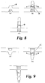
Figure 8 shows an energy level diagram for an n-type device according to the present invention; -
Figure 9 shows an energy level diagram for a p-type device according to the present invention; -
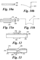
Figure 10a shows a schematic representation of a heterojunction formed from a layer of a first material (narrow band gap semiconductor) and a layer of a second material (wide band gap semiconductor); -
Figure 10b shows the potential distribution across the junction shown inFigure 10a ; -
Figure 11a shows a schematic representation of a heterojunction formed from a layer of a first material (narrow band gap semiconductor) between two layers of a second material (wide band gap semiconductor); -
Figure 11b shows the potential distribution across the junction shown inFigure 11a ; and -
Figure 12 shows a cross section through an alternative structure for fabricating the transistor; -
Figure 13 shows a cross section through a further alternative of the structure of the transistor; -
Figure 14 shows a plan view of the structures ofFigures 12 and 13 ; -
Figure 15 shows a further view of a different possible structure for fabricating the transistor; -
Figure 16 shows still a further structure for fabricating the transistor; and -
Figure 17 shows further details ofFigure 3 . -
Figures 1 and 2 show the prior art wherein a single electron transistor (or unipolar SET) is provided from a heterojunction of typical III-V semiconductor such as GaAs. - In
Figure 1 a device 1 is provided having a layer ofGaAs 2 adjacent a layer of AlxGa1-xAs 4 to form a heterojunction. Afirst gate electrode 6 is provided at a bottom region of the device and a pair ofsecond gate electrodes 8 are provided at a top portion of the device opposite the heterojunction from thefirst gate electrode 6. - Each of the
second gate electrodes 8 comprises an elongate member with twostubs - Electrons can be confined in a direction perpendicular to an axis passing through both of the gate electrodes in a thin sheet in the
GaAs 2 just above the AlxGa1-xAs 4 close to the heterojunction interface. A potential energy profile of this sheet is shown inFigure 2 . - The skilled person will realise that the there are two saddle points caused in the potential energy profile of
Figure 2 which occur in the thin sheet below thestubs -
Figure 2a shows an energy level diagram forFigure 2 . Theconduction band 13 and thevalence band 15 are shown.Peaks gate electrodes region 14 ofFigure 2 is shown to be between the two peaks in theconduction band 13. The skilled person will appreciate that thevalence band 15 is not important in the unipolar SET because of the large band gap (it is so far removed when looking at the energies that it plays no role in the functioning of the device). - The
region 14 of minimal potential is referred to as a quantum dot and the confinement is said to be soft since it is controlled by the voltage on the gate electrodes. Conversely, confinement out of the thin sheet is said to be hard since it is due to the heterojunction step itself. At low temperatures with low bias voltages applied to the gate electrodes the source-drain resistance (in a direction perpendicular to an axis passing between the gate electrodes) will essentially be infinite provided the source-drain voltage difference is small (that is VSD < < e/C where C is the effective capacitance of the dot). - Increasing the gate voltage will lower the barriers (and the position of the well relative to the Fermi energy) and eventually the lowest quasi-bound state in the well will be resonant with the Fermi energy allowing an electron to tunnel into the well. For small voltages applied in the drain source direction a current will flow. This current is due to single electrons moving into and out of the
quantum dot 14. An electron entering the dot from the source must leave the dot before another electron can enter due to the large Coulomb repulsion between two electrons within thedot 14. This is due to the so-called Coulomb blockade. A further increase in the gate voltage will lower the resonant-bound state energy relative to the Fermi energy and thedot 14 will remain charged with a single electron. There is again a barrier to current flow at low temperature. The electron in the dot cannot leave since its energy is below the Fermi energy and a further electron may not enter thedot 14 because of Coulomb repulsion (Coulomb blockade). The current is essentially switched off. A further increase in the gate voltage will eventually lower the potential energy in the dot sufficiently for a second electron to enter thedot 14 giving rise once more to a single-electron current. In this way we get a series of current peaks as the gate voltage is varied with each peak corresponding to fluctuations in electron number of just one in thedot 14. This current is shown schematically inFigure 3 where it should also be noticed that the peaks are approximately equally spaced, which may be explained by an approximate semi-classical charging model in which the separation between peaks is potential V = e/C (Where e is the charge on the electron and C is the capacitance of the dot). These peaks in conductance as a function of gate voltage are referred to as the single electron transistor (SET) oscillations. - Looking at
Figure 3 maximum current will flow through the transistor when the gate voltage equals V1. Should the gate voltage be held at V1 continuous current would flow through the device. As will be evident fromFigure 3 due to the large gradient of the I Vs V curve, when the gate voltage is held at V1, a small change in applied gate voltage causes a large change in current flowing through the transistor (again for VSD < < e/C). - An approximation of a
device 19 according to the present invention is shown inFigure 4 . This simplified structure makes it clear just how the device operates and the structure has been used to explain the concept. - A layer of InAlSb (wide band gap second material) 20 is provided in association with a layer of
InSb 22 forming a heterojunction wherein carriers are hard confined in a thin sheet in the InSb 22 (narrow band gap first material) just above theInAlSb 20 close to the heterojunction interface. Thus, a so called two dimensional electron (or hole) gas is formed near to the heterojunction. - A
first gate 24 electrode is positioned at a first side of the heterojunction and asecond gate electrode 26 comprising a pair of electrodes is positioned at the opposite side of the heterojunction. Each one of thesecond gate electrodes 26 comprises an elongated metallic electrode. Adrain 28 and asource 30 electrode are positioned at either end of layers ofInSb 22 and InAlSb 20 (along a plane running parallel to the heterojunction). - A
third gate electrode 34 which in this case is circular (but in other embodiments could be of a different shape, such as a cube or rectangle) is positioned between thesecond gate electrodes 26. - The size of the
third electrode 34 and spacing from thesecond gate electrodes 26 is critical to the operation of the device. Clearly, the geometry of theelectrodes - In use a potential applied to the first, second and
third gate electrodes Figure 5 . (The position of thedrain 28 and thesource 30 electrodes are shown at either end ofFigure 5 to show the orientation of the Figure relative to the device shown inFigure 4 ). The graph shows the potential along a two dimensional plane in the InSb close to the heterojunction. The z-axis of the graph represents the potential at each point on the plane. - In, operation, (for an n-type device) the second and
third electrodes first electrode 24. Furthermore, the bias on thethird electrode 34 would be most negative. [Conversely, for a p-type device on the second andthird electrodes first electrode 24, with thethird electrode 34 being most positive]. - Looking at
Figure 5 , the field due to the potential applied between the first andsecond electrodes gulley 35. The field due to the potential applied between the first andthird electrodes potential barrier 37.Figure 5 is for an n-type device. Similarly a p-type device would have a central potential well. - A potential is also applied between the
drain 28 andsource 30 electrodes (VSD). The skilled person will appreciate that VSD causes a slight bias on electrons within the transistor causing them to tend to move towards thedrain 28 electrode. When an electron is within thepotential barrier 37 it may Zener tunnel out of thebarrier 37 either toward thesource 30 or drain 28 electrodes. Without VSD being applied there would be an equal chance of either direction occurring. However, VSD increases the probability of electrons tunnelling out of thebarrier 37 in the direction of thedrain 28 electrode. - VSD is necessarily small and has a maximum magnitude of substantially kT (approximately 25meV at room temperature). Should VSD have too large a magnitude electrons will pass through the
potential barrier 37 without being held inside. - At a central portion of the potential energy field there is a maximum of potential which occurs near the heterojunction in a region below the third gate electrode 34 (At 37 in
Figure 5 ). As with the device ofFigure 1 , as the potential applied between the first 24 and third 34 gate electrodes is varied the height of the maximum 37 is altered. Also, varying the potential applied between the first and second 24, 26 gate electrodes causes the depth of thegulley 35 to be varied, by varying the magnitude of the edge portions of the gulley. - The skilled person will realise that in
Figure 2 there were two potential barriers between which an electron could be held (in a quantum dot) whereas inFigure 5 at 37 there is only a single electron potential energy maximum. However, as will now be described the device ofFigure 4 can be made to operate in a similar manner to that of the device ofFigure 1 . - The
device 19 makes use of the narrow band gap of less than 0.5eV which exists in materials such as InSb and CdxHg1-xTe. That is the energy level of the valence band is relatively close to the energy level of the conduction band when compared to other III-V semiconductor such as GaAs and InAs. - When looking at the physics of the device shown in
Figure 1 , because of the large band gap between the valence and the conduction bands, the valence band can be ignored in an n-type device. As shown inFigure 2 electrons are trapped in a quantum dot formed between two peaks in the conduction band of the heterojunction. - However, in the device of
Figure 4 the valence band cannot be ignored and energy level diagrams are shown inFigures 9 to 10 . - A material used for this embodiment has a narrow band gap. That is, the valence band is at an appropriate level to complement the conduction band so that electrons can use the valence band to tunnel.
- If a bias voltage is applied to the
gate electrodes gate electrode 34 the energy of the valence band edge below this gate can be higher than the conduction band edge at a point along thegulley 35. - This process is shown in
Figure 8 for a device fabricated in n-type material wherein the majority charge carriers are electrons. Applying a negative voltage to the third gate electrode, 34 raises both the valence and conduction bands and asingle hump 36 appears in the energy band diagram (Figure 8a ). The important point to notice is that due to the high confinement, the region under the barrier in the valence band gives rise to discrete energy levels. When the Fermi energy lies above the highest level, the resistance will be effectively infinite at small biases. - In
Figure 8b a larger negative bias voltage has been applied to thegate electrode 34 raising the valence band above the conduction band in a position along thegulley 35. At a certain bias voltage, the energy of alevel 38 within the valence band will be coincident with the Fermi energy and electrons will be able to tunnel into and out of this energy level 38 (represented by the line and unfilled circle). Because of Coulomb repulsion between the electrons and quantisation of the energy levels only a single electron at a time can enter theenergy level 38. - Because tunnelling from conduction band to valence band is known as Zener tunnelling we refer to this device as a Zener single-electron transistor (Zener SET).
-
Figure 8c shows that if a further bias voltage (is made more negative) is applied to thegate electrode 34 then theenergy level 38 moves above the Fermi energy and electrons can no longer tunnel across the heterojunction. Therefore, the device ofFigures 4 ,6, and 7 operates in a manner similar to that of the device ofFigure 1 and current flows as is shown inFigure 3 . There is a large gap between the unoccupied level in the dot and the next (unoccupied) level, representing both the quantisation gap of the single-electron states, due to confinement and the Coulomb blockade energy (energy of repulsion between two charge carriers in the dot). Note, however, that for the conventional SET the gate bias is increased whereas for the Zener SET it is decreased. - As the skilled person will appreciate there exist both heavy and light holes within the valence band. The separation of the holes is proportional to the reciprocal of the effective mass and therefore the heavy holes have a smaller separation. Electrons only have a single effective mass and this is equal to the mass of a light hole.
- As electrons tunnel into the valence band they can occupy heavy or light holes. Coulomb blockade will effect the electrons in the same way regardless of whether heavy or light hole states have been occupied and prevent more than one electrons occupying that particular hole state.
- It is desirable for the electrons to occupy light hole states due to the larger energy gap between these hole states meaning that the transistor is less influenced by changes in temperature. As the temperature increases so does the probability that an electron in the
gulley 35 region be thermally excited above the Fermi energy. Should the electrons energy become coincident with that of the hole state conduction will occur. Since the light holes have a larger energy separation more temperature change is likely to be needed to equate the energy of the hole state to the energy of the thermally excited electron in thegulley 35. - By applying a physical elastic strain it is possible to shift the heavy and light hole bands apart, reducing the energy levels of the heavy holes so that only light holes can be used for tunnelling. It is possible using the wide, narrow, wide band gap structure discussed hereinafter to apply a permanent strain to the material.
- The skilled person will realise that the wide band gap structure has a small lattice spacing. By growing the narrow band gap structure thin enough in association with the wide band gap material it is possible to ensure the lattice matching causes a permanent compression throughout the narrow layer. This ensures only the light holes are utilised for tunnelling. That is, the lattice of the narrow band gap material must match the lattice of the wide band gap material at the interface; because the wide gap has the smaller spacing the narrow gap material will be strained by the matching of the lattices.
- The skilled person will also appreciate that as an electron tunnels into the valence band, the energy gap to hole states above the Fermi energy within the valence band effectively increases (due to Coulomb blockade).
-
Figure 9 shows a similar energy level diagram toFigure 8 but for a device fabricated from p-type material wherein the majority charge carriers are holes. In this situation if a sufficiently large positive bias is applied to thegate electrode 34 the conduction band edge below this gate electrode may become lower than the Fermi energy. - Once the
energy level 40 becomes coincident with the Fermi level electrons can Zener tunnel from the valence band into the quantum confined conduction band region. This is equivalent to holes Zener tunnelling out of the quantum confined region into the valence band (Figure 9b ). If the bias voltage is further increased theenergy level 40 drops below the Fermi energy and electrons can no longer tunnel across the heterojunction. - Such a p-type SET has the advantage over the unstrained n-type SET of enhanced quantisation in the confined region due to the lower effective mass of the conduction-band electrons.
- A quantum dot, such as occurs in the confined region of a SET, behaves in some ways like an atom showing, for example, electron affinity, and ionisation in the Coulomb blockade regime, where at low-temperatures the quantum dot will have an integral number of charge carriers. It has been suggested that a quantum dot may be referred to as an 'artificial atom'. (Dots occupied with one, two, three ... electrons being artificial H, He, Li respectively...). Two artificial atoms in series will be the analogue of molecules. For the Zener set such a molecule may be fabricated by creating two barriers as was done for the single SET in GaAs. A typical conduction band edge profile would be similar to that for the single SET in GaAs but the device would behave quite differently due to the presence or resonant levels in both the valence bands (barrier regions) and conduction band (well region).
- Finally, there is one further fundamental difference between the Zener SET and the conventional SET. In the latter, the tunnelling barriers into and out of the quantum dot must have high resistance (> > the resistance quantum ≈ 13kQ) in order to have strong confinement. If this were not the case then the resonant bound state would be broadened, the Coulomb blockade reduced and the device would always be switched on. This need not be the case for the Zener SET. Provided the single barrier is sufficiently strong the device will be essentially 'off' at the appropriate gate bias since the tunnelling of conduction electrons will be small (
Figure 9a ). However, when the barrier height is increased by applying a negative bias to the gate, the Zener tunnelling barriers need not be strong in order for the transistor to switch on. These Zener barriers may be 'tuned' by choice of semi-conductor and geometry. For weak barriers the current through the device will be relatively large, significant 'co-tunnelling' will take place and the fluctuations in electron number on the quantum dot may well exceed unity. This will also cause the `turn on' to be more gradual and will reduce the Coulomb blockade, resulting in weaker SET oscillations. However, this mode may be preferable for some applications where a low 'on' resistance is required. Conversely, for strong Zener barriers, the turn-on will be sharp and the subsequent SET oscillations sharp, as with the unipolar device. - The device shown in
Figure 4 is of a simplified nature so that the principles of operation can be more easily explained. However, a more realistic device structure is shown inFigures 6 and 7 . - A heterojunction is formed by a 20nm thick layer of InAlSb (wide band gap second material) 100 provided in association with a 20nm thick layer of InSb (narrow band gap first material) 102. The sheet of electrons are maintained by the heterojunction in a thin layer in the InSb layer near to the junction. This is to prevent tunnelling of electrons from the second and third gates into the InSb.
- A
source electrode 106 and adrain electrode 108 are provided at each end of the heterojunction on top of theInSb 102 layer. Between thesource 106 and thedrain 108 there is provided a layer ofinsulation 104, in this case SiO2, on top of theInSb 102 layer. - At each side of the device, on top of the
InSb 102 layer, there is provided aside gate electrode side gate electrodes InSb layer 102. On top of each of the side gate electrodes there is provided a fillet of SiO2 insulation 114, 116 which insulate asecond gate electrode 118, in the shape of a bow tie, from theside gate electrodes - In the preferred embodiment the electrodes are fabricated from gold on top of a layer of chromium. The chromium ensures the gold adheres to the transistor. However, the choice of materials for the electrodes is not critical.
- The two
side gates central region 120 of the transistor and thus thecentral region 120 is not covered by theside gates second gate electrode 118 is arranged to be over thecentral region 120 of the transistor. This central region of the gate transmits a much larger voltage to the InSb than elsewhere since it is not screened by the SiO2 fillet. This can be most clearly seen inFigure 7 . - At an underneath of the transistor, as viewed in
Figure 7 , there is provided afirst gate electrode 124. As with the device ofFigure 4 applying bias voltages between the first andsecond gate electrodes - The
side gate electrodes regions Figure 5 ) so as to ensure that electrons cannot be transmitted through this portion, but not too high, otherwise electrons could Zener tunnel from the central region, out of the gulley towardelectrodes side gate electrodes gulley 35; a compromise value ensuring electrons can not bypass thepotential maxima 37, nor tunnel out of thegulley 35 towardsregions - The skilled person will appreciate that the heterojunction can be formed by a variety of different methods, which are represented in
Figures 10 and 11 . In the previous figures the structure ofFigure 10a has been described with a layer of InSb (narrow band gap semi-conductor) 102, adjacent a layer of InAlSb (wide band gap semi-conductor) 100. This structure provides the potential profile shown inFigure 10b . Electrons are held at the minimum of potential (shown at 200). However, should the potential profile be too shallow the confinement of the electrons within the thin sheet of charge near the heterojunction will not be strong and electrons can easily escape out of the plane of charge.Figure 10a is a simplification of the earlier Figures and oxide layers and gates would be provided in addition to thelayers -
Figure 11a shows an alternative structure for the heterojunction wherein alayer 202 of InSb (narrow band gap semi-conductor) has been provided between two layers of InAlSb (wide band gap semiconductor) 204, 206. The layer ofInSb 202 is narrower than the layers ofInAlSb layer 202 have significant thickness then two heterojunctions would be provided in series. However, the thickness of theInSb layer 102 cannot be too small because it becomes hard to fabricate and also the charge capacity (i.e. the number of electrons that thelayer 102 can physically hold) becomes too small. In this embodiment the preferred thickness is 20nm. -
Figure 11a also shows anoxide layer 208 that has been grown on top of theInAlSb layer 204. Thisoxide layer 208 may be necessary to remove material mismatch problems between atop gate electrode 210 and theInAlSb layer 204. Abottom gate electrode 212 is also shown. -
Figure 11b shows the potential profile for the heterojunction formed by the structure ofFigure 11a . Rather than relying on the minimum of potential to hold electrons in theregion 200 there is now a defined well 214 in which electrons are held. It does not matter whether or not the potential profile is too shallow; electrons will still be maintained within the thin sheet of charge in the vicinity of the heterojunction. - The structure of
Figure 11a may be preferred over the structure ofFigure 10a in view of a cleaner junction interface at the top junction resulting in a higher carrier mobility. - A two dimensional electron sheet could also be provided by the use of modulation doping in a layer of wide band gap semionductor adjacent a layer of narrow band gap semiconductor as will be appreciated by the skilled person.
- The devices of
Figures 4 and6 rely on soft confinement (the provision of electric fields) to maintain electrons within the electron sheet provided by the heterojunction in a narrow strip or quantum wire. As the skilled person will appreciate hard confinement wherein the electrons are controlled by physical barriers to form a quantum wire is also possible. Such structures are shown inFigures 12 to 16 . -
Figure 12 shows a first possibility wherein a layer of second material, or wideband gap semionductor 250 is provided on top of asubstrate 252 which would generally be an n+ material. A narrow strip of narrowband gap semiconductor 254, or first material is provided on top of the wide band gap material. Generally this would be provided by depositing a layer of narrow band gap material onto the wide band gap material and then etching the narrow band gap material to the desired width. - Both the narrow
band gap strip 254 and the wideband gap layer 250 are covered in a layer ofinsulator 256, in this case silicon dioxide. Asecond gate electrode 258 is provided which as can be seen inFigure 14 is a bow tie shape having aprimary portion 260, approximately 50nm in width, which extends over the strip of narrow band gap material 254 (shown in outline). - A
first electrode 262 is provided on the underside of thesubstrate 252. Also seen inFigure 14 are third and fourth electrodes 261,263 which form drain and source electrodes. - The device of
Figure 12 would operate in the same manner as those ofFigures 4 and6 except that are no side gates to which a potential must be applied. The electrons / holes are maintained in a strip due to the structure of the device. The quantum dot is provided within the strip of charge carriers by a potential applied between the first 262 and the second 258 gate electrodes. -
Figure 13 shows a further structure for a transistor according to the invention which, as with the device ofFigure 12 , relies on hard confinement to provide a quantum wire. - A
substrate 270 is provided in which there is a V shapedgroove 272. A layer of wideband gap semiconductor 274 or second material is provided on top of the substrate which covers the surface of thegroove 272. As the skilled person will appreciate the V of the groove in thesubstrate 270 will not be perfectly sharp but will be rounded. The layer of the wideband gap material 274 will also have a rounded V, as can be seen inFigure 17 . -
Figure 17 shows an enlargement of thegroove 272 ofFigure 13 where asubstrate 270 is shown with thegroove 272 fabricated therein. The groove has a rounded V portion. Alayer 274 of second material has been deposited on thesubstrate 270 The lattice planes of second material at the edge portion of the V are < 111 > compared to < 001 > planes at surface regions outside thegroove 272. The first material grows faster on the < 001 > planes during deposition and therefore a thin coating offirst material 276 can be provided which is concentrated in the base of thegroove 272. The groove is then filled with aninsulator 278. The process can be repeated so a number of wires are provided vertically above one another. - A region of narrow
band gap semionductor 276, or first material, is deposited on top of the layer of wideband gap semiconductor 274. Due to the alignment of the lattice planes in the wide band gap semiconductor the narrow band gap semiconductor is preferentially deposited in the V of the groove forming theregion 276. It will be appreciated that a thin layer of the narrow band gap semiconductor will be present on the sides of the groove, but the material will be concentrated in the V of the groove. - A layer of
insulation 278 is provided which fills the groove and covers the layer of wide band gap material. As will be appreciated although the narrow bad gap semiconductor is preferentially deposited in the V of the groove, a thin layer of narrow band gap semiconductor is likely to be present on the sides of the groove and will thus be sandwiched between the wideband gap semiconductor 274 and theinsulator 278. On top of the layer of insulation there is provided asecond gate electrode 280. As the previous embodiments afirst gate electrode 282 is provided underneath thesubstrate 270. - The structure of
Figure 13 is also shown in plan inFigure 14 , wherein thesecond electrode 280 can be seen to have the bow tie structure with aprimary portion 260 overlying the groove (shown in outline) and consequently the region of first material. - The device of
Figure 13 will operate in the same manner as the device ofFigure 12 . - Yet a further alternative structure for providing a transistor according to the invention is shown in
Figure 15 . In this structure a wafer of intrinsic wide bandgap semi conductor 290 is provided. This wafer has been cut at an angle (possibly at up to substantially 6°) to a plane wherein the atoms in the lattice are aligned. This provides a stepped surface as can be seen in the Figure. - A layer of narrow band gap semiconductor, or first material, is deposited on to the wide
band gap material 290. Due to the stepped structure in the wideband gap material 290 the narrow band gap material is preferentially deposited in base regions of thesteps 292 and thus regions of the narrowband gap semiconductor 294 are provided. It will be appreciated that the narrow band gap semiconductor will cover the wide band gap semiconductor but theregions 294 are of much greater thickness due to the preferential deposition. - A layer of
insulator 296 is provided which covers the narrow band gap semiconductor and asecond electrode 298 is provided on top of the insulator. Again afirst electrode 300 is provided underneath the structure. - The device of
Figure 15 functions in a similar manner to the device described in relation toFigures 12 and 13 . -
Figure 16 shows a further alternative structure for fabricating the transistor relying on hard confinement of electrons. Asubstrate 302 is etched withreverse mesa stripes 304 providing a plurality ofridges 306. The etching is such that sharp regions 308 are provided at end portions of theridges 306. - The lattice structure is such that when further layers are deposited onto the ridges the deposition process is much more rapid on the side walls than at the sharp region 308. A wide band gap material is deposited on to the
ridge 306 forming alayer 310. A layer of narrowband gap material 312 is deposited on to the wideband gap material 310. When the narrow band gap material is deposited the differential deposition rates are exploited so that primarily only a region of narrow band gap material exists at the top most region of theridge 306. The structure is subsequently covered in an insulatinglayer 314. The insulation may completely fill the reverse mesa. - Gate electrodes are provided in the same manner as in
Figures 12, 13 ,15 and the device operates in a similar manner.
Claims (21)
- A field effect single charge carrier transistor (19) comprising a heterojunction formed between layers of a first semiconductor material (22, 102, 202, 254, 276, 294, 312) and a second semiconductor material (20, 100, 204, 206, 250, 274, 310); and a first gate electrode (24, 124, 212, 262, 282, 300) provided on a first side of the heterojunction;
wherein a second gate electrode (34, 118, 210, 258, 280, 298) is provided on a second side of the heterojunction which is on the opposite side of the heterojunction from the first side; the first layer of semiconductor material having a bandgap of less than 0.5eV and valence and conduction bands having sufficiently similar energy levels such that the top region of the valence band, respectively the bottom region of the conduction band, at one point within the transistor can be forced in open how to be higher in electron energy, respectively lower in electron energy, than the bottom region of the conduction band, respectively the top region of the valence band, at another point within the transistor by applying a potential to said first and second gate electrodes causing a controllable single potential barrier, respectively a controllable single potential well, to be provided at said one point along a quantum wire in the potential field within a sheet of charge carriers in said first semiconductor material near said heterojunction, energy states within the valence band of said potential barrier, respectively within the conduction band of said potential well, being occupied by charge carriers tunneling in said valence band, respectively in said conduction band, the tunneling being Zener tunneling. - A transistor according to Claim 1 wherein the heterojunction is provided as a single layer of said first semiconductor material (102, 254, 276, 294, 312) adjacent a single layer of said second semiconductor material (100, 250, 274, 290, 310).
- A transistor according to Claim 1 wherein the heterojunction is provided as single layer of said first semiconductor material (202) between two layers of said second semiconductor material (204,206).
- A transistor according to any one of Claims 1 to 3 wherein said first semiconductor material is one of Insb and CdxHg1-xTe.
- A transistor according to any one of Claims 1 to 4 in which said second semiconductor material is one of InAISb, CdxHg1-xTe and CdTe.
- A transistor according to any preceding claim wherein the second gate electrode (118, 210, 258, 280, 298) is insulated from he materials forming the heterojunction by at least a single layer of insulation (114, 116, 208, 256, 278, 296, 314).
- A transistor according to any preceding claim wherein one or more side gates (26,110,112 ) are provided.
- A transistor according to Claim 7 wherein the or each side gate comprises an elongate area along one side of said first or second semiconductor material above the heterojunction.
- A transistor according to any preceding claim wherein two side gates (26,110,112) are provided.
- A transistor according to Claim 9 wherein the two side gates are in the same plane and there exists a gap (120) within that plane between the two areas of side gates.
- A transistor according to any one of Claims 7 to 10 wherein the second gate electrode (118) is provided above and insulated from the or each side gate.
- A transistor according to Claim 10 wherein the second gate electrode (118) comprises a central portion (122) which extends over the gap (120) between the side gates.
- A transistor according to Claim 1 wherein the heterojunction is provided between a strip of said first semiconductor material (254) and a layer of said second semiconductor material (250).
- A transistor according to Claim 13 wherein said second gate electrode (258) is provided overlying the strip of first material (254).
- A transistor according to Claim 1 wherein the transistor contains a V shaped notch or groove (272) within a substrate (270).
- A transistor according to Claim 15 wherein a layer (274) of said second semiconductor material is provided lining the groove.
- A transistor according to Claim 16 wherein a region (276) of said first semiconductor material is provided in the V of the notch of the lined groove.
- A transistor according to Claim 1 wherein the transistor has a layer of said second semiconductor material (290) having a non planar surface upon which a quantum wire (294) has been fabricated.
- A transistor according to Claim 18 wherein the substrate has a surface which has steps (292) due to being cut off axis to a planar plane of the crystal lattice.
- A transistor according to Claim 1 wherein the transistor comprises at least one ridge (306) grown quantum wire (312).
- A method of detection comprising using a charge detector wherein the gate electrodes of a field effect transistor according to any of Claims 1 to 20 are connected to a potential source which is representative of the quantity being detected such that variations in the quantity causes variations in the potential applied to the gate electrodes which, in turn, causes a change in current flowing through the transistor.
Applications Claiming Priority (3)
| Application Number | Priority Date | Filing Date | Title |
|---|---|---|---|
| GB9813142 | 1998-06-19 | ||
| GB9813142A GB2338592A (en) | 1998-06-19 | 1998-06-19 | Single electron transistor |
| PCT/GB1999/001885 WO1999066561A1 (en) | 1998-06-19 | 1999-06-18 | Single charge carrier transistor, method of holding a charge carrier within a quantum dot, and method of detection |
Publications (2)
| Publication Number | Publication Date |
|---|---|
| EP1088347A1 EP1088347A1 (en) | 2001-04-04 |
| EP1088347B1 true EP1088347B1 (en) | 2011-11-23 |
Family
ID=10833967
Family Applications (2)
| Application Number | Title | Priority Date | Filing Date |
|---|---|---|---|
| EP99928062A Withdrawn EP1088346A1 (en) | 1998-06-19 | 1999-06-18 | Quantum wire field-effect transistor and method of making the same |
| EP99957113A Expired - Lifetime EP1088347B1 (en) | 1998-06-19 | 1999-06-18 | Single charge carrier transistor and detection method using the same |
Family Applications Before (1)
| Application Number | Title | Priority Date | Filing Date |
|---|---|---|---|
| EP99928062A Withdrawn EP1088346A1 (en) | 1998-06-19 | 1999-06-18 | Quantum wire field-effect transistor and method of making the same |
Country Status (5)
| Country | Link |
|---|---|
| US (2) | US6753593B1 (en) |
| EP (2) | EP1088346A1 (en) |
| JP (2) | JP4864202B2 (en) |
| GB (1) | GB2338592A (en) |
| WO (2) | WO1999066562A1 (en) |
Families Citing this family (29)
| Publication number | Priority date | Publication date | Assignee | Title |
|---|---|---|---|---|
| WO2003005450A2 (en) * | 2001-05-18 | 2003-01-16 | President And Fellows Of Harvard College | Nanoscale wires and related devices |
| US6683337B2 (en) | 2001-02-09 | 2004-01-27 | Micron Technology, Inc. | Dynamic memory based on single electron storage |
| US6978070B1 (en) * | 2001-08-14 | 2005-12-20 | The Programmable Matter Corporation | Fiber incorporating quantum dots as programmable dopants |
| JP4334246B2 (en) | 2003-02-27 | 2009-09-30 | 富士通株式会社 | Quantum semiconductor device and manufacturing method thereof |
| JP4304338B2 (en) * | 2004-01-13 | 2009-07-29 | 独立行政法人産業技術総合研究所 | Photodetector |
| US7692180B2 (en) | 2004-06-04 | 2010-04-06 | Ravenbrick Llc | Layered composite film incorporating quantum dots as programmable dopants |
| US7465595B2 (en) | 2004-11-09 | 2008-12-16 | Fujitsu Limited | Quantum device, manufacturing method of the same and controlling method of the same |
| US7759699B2 (en) * | 2005-07-06 | 2010-07-20 | International Rectifier Corporation | III-nitride enhancement mode devices |
| US7358581B2 (en) * | 2005-11-17 | 2008-04-15 | Kulite Semiconductor Products, Inc. | Quantum dot based pressure switch |
| US20070194297A1 (en) * | 2006-02-17 | 2007-08-23 | The Programmable Matter Corporation | Quantum Dot Switching Device |
| US7601946B2 (en) * | 2006-09-12 | 2009-10-13 | Ravenbrick, Llc | Electromagnetic sensor incorporating quantum confinement structures |
| JP5399923B2 (en) | 2007-01-24 | 2014-01-29 | レイブンブリック,エルエルシー | Temperature response switching type optical down-converting filter |
| US8363307B2 (en) * | 2007-02-28 | 2013-01-29 | Ravenbrick, Llc | Multicolor light emitting device incorporating tunable quantum confinement devices |
| US7936500B2 (en) * | 2007-03-02 | 2011-05-03 | Ravenbrick Llc | Wavelength-specific optical switch |
| KR101265393B1 (en) | 2007-07-11 | 2013-05-20 | 라벤브릭 엘엘씨 | Thermally switched reflective optical shutter |
| CN101868738B (en) | 2007-09-19 | 2013-05-15 | 雷文布里克有限责任公司 | Low-emissivity window films and coatings incorporating nanoscale wire grids |
| US8169685B2 (en) | 2007-12-20 | 2012-05-01 | Ravenbrick, Llc | Thermally switched absorptive window shutter |
| CN102066992B (en) | 2008-04-23 | 2013-11-13 | 雷文布里克有限责任公司 | Glare management of reflective and thermoreflective surfaces |
| US9116302B2 (en) | 2008-06-19 | 2015-08-25 | Ravenbrick Llc | Optical metapolarizer device |
| US8665414B2 (en) | 2008-08-20 | 2014-03-04 | Ravenbrick Llc | Methods for fabricating thermochromic filters |
| CN102460238A (en) | 2009-04-10 | 2012-05-16 | 雷文布里克有限责任公司 | Thermally switched optical filter incorporating a guest-host architecture |
| US8867132B2 (en) * | 2009-10-30 | 2014-10-21 | Ravenbrick Llc | Thermochromic filters and stopband filters for use with same |
| WO2011062708A2 (en) | 2009-11-17 | 2011-05-26 | Ravenbrick Llc | Thermally switched optical filter incorporating a refractive optical structure |
| CN103038701B (en) | 2010-03-29 | 2017-01-18 | 雷文布里克有限责任公司 | Polymer-stabilized thermotropic liquid crystal device |
| GB2480265B (en) * | 2010-05-10 | 2013-10-02 | Toshiba Res Europ Ltd | A semiconductor device and a method of fabricating a semiconductor device |
| EP2576934A4 (en) | 2010-06-01 | 2014-01-01 | Ravenbrick Llc | Multifunctional building component |
| US8933488B2 (en) * | 2010-12-03 | 2015-01-13 | The Board Of Trustees Of The Leland Stanford Junior Univerity | Heterostructure field effect transistor with same channel and barrier configuration for PMOS and NMOS |
| WO2013033608A2 (en) | 2011-09-01 | 2013-03-07 | Wil Mccarthy | Thermotropic optical shutter incorporating coatable polarizers |
| US9859409B2 (en) * | 2016-04-28 | 2018-01-02 | International Business Machines Corporation | Single-electron transistor with wrap-around gate |
Family Cites Families (16)
| Publication number | Priority date | Publication date | Assignee | Title |
|---|---|---|---|---|
| CA1315865C (en) * | 1988-02-09 | 1993-04-06 | Elyahou Kapon | Semiconductor super lattice heterostructure fabrication methods, structures and devices |
| US5497015A (en) | 1988-11-12 | 1996-03-05 | Sony Corporation | Quantum interference transistor |
| EP0386388A1 (en) * | 1989-03-10 | 1990-09-12 | International Business Machines Corporation | Method for the epitaxial growth of a semiconductor structure |
| EP0661733A2 (en) * | 1993-12-21 | 1995-07-05 | International Business Machines Corporation | One dimensional silicon quantum wire devices and the method of manufacture thereof |
| GB2288274A (en) * | 1994-03-31 | 1995-10-11 | Sharp Kk | Quantum device and method of making such a device |
| JPH07326730A (en) * | 1994-05-31 | 1995-12-12 | Mitsubishi Electric Corp | Semiconductor device, unit electronic device and manufacturing method thereof |
| JP3256091B2 (en) * | 1994-08-23 | 2002-02-12 | 株式会社日立製作所 | Crystal grain forming method and semiconductor device |
| US5654558A (en) * | 1994-11-14 | 1997-08-05 | The United States Of America As Represented By The Secretary Of The Navy | Interband lateral resonant tunneling transistor |
| GB2295272B (en) * | 1994-11-15 | 1998-01-14 | Toshiba Cambridge Res Center | Semiconductor device |
| JP3837674B2 (en) * | 1995-03-20 | 2006-10-25 | 富士通株式会社 | Quantum semiconductor device |
| DE19522351A1 (en) * | 1995-06-20 | 1997-01-09 | Max Planck Gesellschaft | Process for producing quantum structures, in particular quantum dots and tunnel barriers, and components with such quantum structures |
| JPH1093109A (en) * | 1996-09-13 | 1998-04-10 | Nippon Telegr & Teleph Corp <Ntt> | Coulomb blockade element and manufacture thereof |
| US5945686A (en) * | 1997-04-28 | 1999-08-31 | Hitachi, Ltd. | Tunneling electronic device |
| KR100240629B1 (en) * | 1997-08-30 | 2000-01-15 | 정선종 | The charging effect nano transistor for tera bit memory devices and method of manufacturing the same |
| KR19990024760A (en) * | 1997-09-08 | 1999-04-06 | 정선종 | Quantum thin wire manufacturing method |
| US6063688A (en) * | 1997-09-29 | 2000-05-16 | Intel Corporation | Fabrication of deep submicron structures and quantum wire transistors using hard-mask transistor width definition |
-
1998
- 1998-06-19 GB GB9813142A patent/GB2338592A/en not_active Withdrawn
-
1999
- 1999-06-18 EP EP99928062A patent/EP1088346A1/en not_active Withdrawn
- 1999-06-18 JP JP2000555299A patent/JP4864202B2/en not_active Expired - Fee Related
- 1999-06-18 EP EP99957113A patent/EP1088347B1/en not_active Expired - Lifetime
- 1999-06-18 WO PCT/GB1999/001940 patent/WO1999066562A1/en active Application Filing
- 1999-06-18 US US09/701,884 patent/US6753593B1/en not_active Expired - Lifetime
- 1999-06-18 WO PCT/GB1999/001885 patent/WO1999066561A1/en active Application Filing
- 1999-06-18 US US09/719,484 patent/US6498354B1/en not_active Expired - Fee Related
- 1999-06-18 JP JP2000555300A patent/JP2002518851A/en not_active Abandoned
Also Published As
| Publication number | Publication date |
|---|---|
| JP2002518851A (en) | 2002-06-25 |
| EP1088346A1 (en) | 2001-04-04 |
| EP1088347A1 (en) | 2001-04-04 |
| WO1999066562A1 (en) | 1999-12-23 |
| JP2002518850A (en) | 2002-06-25 |
| JP4864202B2 (en) | 2012-02-01 |
| WO1999066561A1 (en) | 1999-12-23 |
| US6498354B1 (en) | 2002-12-24 |
| GB9813142D0 (en) | 1998-08-19 |
| GB2338592A (en) | 1999-12-22 |
| US6753593B1 (en) | 2004-06-22 |
Similar Documents
| Publication | Publication Date | Title |
|---|---|---|
| EP1088347B1 (en) | Single charge carrier transistor and detection method using the same | |
| US4575924A (en) | Process for fabricating quantum-well devices utilizing etch and refill techniques | |
| US5701016A (en) | Semiconductor device and method for its manufacture | |
| US4581621A (en) | Quantum device output switch | |
| US5923046A (en) | Quantum dot memory cell | |
| EP0177374B1 (en) | High-speed semiconductor device | |
| JP3745015B2 (en) | Electronic devices | |
| US4912531A (en) | Three-terminal quantum device | |
| US4721983A (en) | Three terminal tunneling device | |
| US4704622A (en) | Negative transconductance device | |
| JPS6327065A (en) | Hetero-junction double-channel semiconductor device, field effect transistor to which the device is applied and apparatus with negative conductance to which the semiconductor is applied | |
| JP2781021B2 (en) | Magnetic field sensor | |
| US5932889A (en) | Semiconductor device with floating quantum box | |
| US4783427A (en) | Process for fabricating quantum-well devices | |
| US5032877A (en) | Quantum-coupled ROM | |
| US4799091A (en) | Quantum device output switch | |
| US5986291A (en) | Field effect devices | |
| US4959696A (en) | Three terminal tunneling device and method | |
| CA2442127C (en) | Negative-resistance field-effect element | |
| US4645707A (en) | Semiconductor devices | |
| JPS639388B2 (en) | ||
| US4969018A (en) | Quantum-well logic using self-generated potentials | |
| EP0545255B1 (en) | Quantum semiconductor device employing quantum boxes for enabling compact size and high-speed operation | |
| EP0170044B1 (en) | Quantum-coupled device | |
| KR100199024B1 (en) | Resonant penetrating transistor with two asymmetric quantum dot |
Legal Events
| Date | Code | Title | Description |
|---|---|---|---|
| PUAI | Public reference made under article 153(3) epc to a published international application that has entered the european phase |
Free format text: ORIGINAL CODE: 0009012 |
|
| 17P | Request for examination filed |
Effective date: 20001202 |
|
| AK | Designated contracting states |
Kind code of ref document: A1 Designated state(s): DE FR GB |
|
| RAP1 | Party data changed (applicant data changed or rights of an application transferred) |
Owner name: QINETIQ LIMITED |
|
| 17Q | First examination report despatched |
Effective date: 20080204 |
|
| RAP1 | Party data changed (applicant data changed or rights of an application transferred) |
Owner name: QINETIQ LIMITED |
|
| GRAP | Despatch of communication of intention to grant a patent |
Free format text: ORIGINAL CODE: EPIDOSNIGR1 |
|
| RTI1 | Title (correction) |
Free format text: SINGLE CHARGE CARRIER TRANSISTOR AND DETECTION METHOD USING THE SAME |
|
| GRAS | Grant fee paid |
Free format text: ORIGINAL CODE: EPIDOSNIGR3 |
|
| GRAA | (expected) grant |
Free format text: ORIGINAL CODE: 0009210 |
|
| AK | Designated contracting states |
Kind code of ref document: B1 Designated state(s): DE FR GB |
|
| REG | Reference to a national code |
Ref country code: GB Ref legal event code: FG4D |
|
| REG | Reference to a national code |
Ref country code: DE Ref legal event code: R096 Ref document number: 69943880 Country of ref document: DE Effective date: 20120202 |
|
| PLBE | No opposition filed within time limit |
Free format text: ORIGINAL CODE: 0009261 |
|
| STAA | Information on the status of an ep patent application or granted ep patent |
Free format text: STATUS: NO OPPOSITION FILED WITHIN TIME LIMIT |
|
| 26N | No opposition filed |
Effective date: 20120824 |
|
| REG | Reference to a national code |
Ref country code: DE Ref legal event code: R097 Ref document number: 69943880 Country of ref document: DE Effective date: 20120824 |
|
| GBPC | Gb: european patent ceased through non-payment of renewal fee |
Effective date: 20120618 |
|
| REG | Reference to a national code |
Ref country code: FR Ref legal event code: ST Effective date: 20130228 |
|
| REG | Reference to a national code |
Ref country code: DE Ref legal event code: R119 Ref document number: 69943880 Country of ref document: DE Effective date: 20130101 |
|
| PG25 | Lapsed in a contracting state [announced via postgrant information from national office to epo] |
Ref country code: DE Free format text: LAPSE BECAUSE OF NON-PAYMENT OF DUE FEES Effective date: 20130101 Ref country code: GB Free format text: LAPSE BECAUSE OF NON-PAYMENT OF DUE FEES Effective date: 20120618 Ref country code: FR Free format text: LAPSE BECAUSE OF NON-PAYMENT OF DUE FEES Effective date: 20120702 |