EP1087253B1 - Flüssigkristallvorrichtung und Verfahren zu deren Herstellung - Google Patents
Flüssigkristallvorrichtung und Verfahren zu deren Herstellung Download PDFInfo
- Publication number
- EP1087253B1 EP1087253B1 EP00307481A EP00307481A EP1087253B1 EP 1087253 B1 EP1087253 B1 EP 1087253B1 EP 00307481 A EP00307481 A EP 00307481A EP 00307481 A EP00307481 A EP 00307481A EP 1087253 B1 EP1087253 B1 EP 1087253B1
- Authority
- EP
- European Patent Office
- Prior art keywords
- liquid crystal
- monomer
- domains
- nematic liquid
- chiral nematic
- Prior art date
- Legal status (The legal status is an assumption and is not a legal conclusion. Google has not performed a legal analysis and makes no representation as to the accuracy of the status listed.)
- Expired - Lifetime
Links
- 239000004973 liquid crystal related substance Substances 0.000 title claims description 151
- 238000004519 manufacturing process Methods 0.000 title 1
- 239000000178 monomer Substances 0.000 claims description 66
- 229920000642 polymer Polymers 0.000 claims description 48
- 239000004986 Cholesteric liquid crystals (ChLC) Substances 0.000 claims description 31
- 239000000758 substrate Substances 0.000 claims description 29
- 238000005191 phase separation Methods 0.000 claims description 24
- 238000001816 cooling Methods 0.000 claims description 16
- 238000000034 method Methods 0.000 claims description 16
- 239000000203 mixture Substances 0.000 claims description 15
- 239000011521 glass Substances 0.000 claims description 10
- 239000004988 Nematic liquid crystal Substances 0.000 claims description 7
- 230000001678 irradiating effect Effects 0.000 claims description 7
- 239000000463 material Substances 0.000 claims description 6
- 239000004305 biphenyl Substances 0.000 claims description 5
- 238000010438 heat treatment Methods 0.000 claims description 5
- QSHDDOUJBYECFT-UHFFFAOYSA-N mercury Chemical compound [Hg] QSHDDOUJBYECFT-UHFFFAOYSA-N 0.000 claims description 5
- 229910052753 mercury Inorganic materials 0.000 claims description 5
- AMGQUBHHOARCQH-UHFFFAOYSA-N indium;oxotin Chemical compound [In].[Sn]=O AMGQUBHHOARCQH-UHFFFAOYSA-N 0.000 claims description 3
- 238000006116 polymerization reaction Methods 0.000 claims description 3
- 238000000399 optical microscopy Methods 0.000 claims description 2
- 238000006467 substitution reaction Methods 0.000 description 16
- 230000003287 optical effect Effects 0.000 description 15
- 230000000007 visual effect Effects 0.000 description 9
- 239000002245 particle Substances 0.000 description 7
- 239000011347 resin Substances 0.000 description 6
- 229920005989 resin Polymers 0.000 description 6
- UWCWUCKPEYNDNV-LBPRGKRZSA-N 2,6-dimethyl-n-[[(2s)-pyrrolidin-2-yl]methyl]aniline Chemical compound CC1=CC=CC(C)=C1NC[C@H]1NCCC1 UWCWUCKPEYNDNV-LBPRGKRZSA-N 0.000 description 5
- 230000005855 radiation Effects 0.000 description 5
- -1 acrylate ester Chemical class 0.000 description 4
- ZUOUZKKEUPVFJK-UHFFFAOYSA-N diphenyl Chemical compound C1=CC=CC=C1C1=CC=CC=C1 ZUOUZKKEUPVFJK-UHFFFAOYSA-N 0.000 description 4
- 230000004313 glare Effects 0.000 description 4
- 230000035939 shock Effects 0.000 description 4
- 125000006850 spacer group Chemical group 0.000 description 4
- XDTMQSROBMDMFD-UHFFFAOYSA-N Cyclohexane Chemical compound C1CCCCC1 XDTMQSROBMDMFD-UHFFFAOYSA-N 0.000 description 3
- 239000002253 acid Substances 0.000 description 3
- WPYMKLBDIGXBTP-UHFFFAOYSA-N benzoic acid Chemical compound OC(=O)C1=CC=CC=C1 WPYMKLBDIGXBTP-UHFFFAOYSA-N 0.000 description 3
- JFDZBHWFFUWGJE-UHFFFAOYSA-N benzonitrile Chemical compound N#CC1=CC=CC=C1 JFDZBHWFFUWGJE-UHFFFAOYSA-N 0.000 description 3
- 210000002858 crystal cell Anatomy 0.000 description 3
- 230000003247 decreasing effect Effects 0.000 description 3
- 239000006185 dispersion Substances 0.000 description 3
- 229920002521 macromolecule Polymers 0.000 description 3
- 239000003505 polymerization initiator Substances 0.000 description 3
- WLPATYNQCGVFFH-UHFFFAOYSA-N 2-phenylbenzonitrile Chemical group N#CC1=CC=CC=C1C1=CC=CC=C1 WLPATYNQCGVFFH-UHFFFAOYSA-N 0.000 description 2
- 239000004983 Polymer Dispersed Liquid Crystal Substances 0.000 description 2
- CZPWVGJYEJSRLH-UHFFFAOYSA-N Pyrimidine Chemical compound C1=CN=CN=C1 CZPWVGJYEJSRLH-UHFFFAOYSA-N 0.000 description 2
- PPBRXRYQALVLMV-UHFFFAOYSA-N Styrene Chemical compound C=CC1=CC=CC=C1 PPBRXRYQALVLMV-UHFFFAOYSA-N 0.000 description 2
- 230000002411 adverse Effects 0.000 description 2
- 125000000217 alkyl group Chemical group 0.000 description 2
- 235000010290 biphenyl Nutrition 0.000 description 2
- 230000003098 cholesteric effect Effects 0.000 description 2
- 150000001875 compounds Chemical class 0.000 description 2
- 239000000470 constituent Substances 0.000 description 2
- 125000000113 cyclohexyl group Chemical group [H]C1([H])C([H])([H])C([H])([H])C([H])(*)C([H])([H])C1([H])[H] 0.000 description 2
- 239000007788 liquid Substances 0.000 description 2
- 125000001997 phenyl group Chemical group [H]C1=C([H])C([H])=C(*)C([H])=C1[H] 0.000 description 2
- 238000004088 simulation Methods 0.000 description 2
- 125000000391 vinyl group Chemical group [H]C([*])=C([H])[H] 0.000 description 2
- 229920002554 vinyl polymer Polymers 0.000 description 2
- OSSNTDFYBPYIEC-UHFFFAOYSA-N 1-ethenylimidazole Chemical compound C=CN1C=CN=C1 OSSNTDFYBPYIEC-UHFFFAOYSA-N 0.000 description 1
- 239000012956 1-hydroxycyclohexylphenyl-ketone Substances 0.000 description 1
- AUXIEQKHXAYAHG-UHFFFAOYSA-N 1-phenylcyclohexane-1-carbonitrile Chemical compound C=1C=CC=CC=1C1(C#N)CCCCC1 AUXIEQKHXAYAHG-UHFFFAOYSA-N 0.000 description 1
- SMZOUWXMTYCWNB-UHFFFAOYSA-N 2-(2-methoxy-5-methylphenyl)ethanamine Chemical compound COC1=CC=C(C)C=C1CCN SMZOUWXMTYCWNB-UHFFFAOYSA-N 0.000 description 1
- NIXOWILDQLNWCW-UHFFFAOYSA-N 2-Propenoic acid Natural products OC(=O)C=C NIXOWILDQLNWCW-UHFFFAOYSA-N 0.000 description 1
- XMLYCEVDHLAQEL-UHFFFAOYSA-N 2-hydroxy-2-methyl-1-phenylpropan-1-one Chemical compound CC(C)(O)C(=O)C1=CC=CC=C1 XMLYCEVDHLAQEL-UHFFFAOYSA-N 0.000 description 1
- BQZJOQXSCSZQPS-UHFFFAOYSA-N 2-methoxy-1,2-diphenylethanone Chemical compound C=1C=CC=CC=1C(OC)C(=O)C1=CC=CC=C1 BQZJOQXSCSZQPS-UHFFFAOYSA-N 0.000 description 1
- WLNDDIWESXCXHM-UHFFFAOYSA-N 2-phenyl-1,4-dioxane Chemical compound C1OCCOC1C1=CC=CC=C1 WLNDDIWESXCXHM-UHFFFAOYSA-N 0.000 description 1
- NIXOWILDQLNWCW-UHFFFAOYSA-M Acrylate Chemical compound [O-]C(=O)C=C NIXOWILDQLNWCW-UHFFFAOYSA-M 0.000 description 1
- 239000005711 Benzoic acid Substances 0.000 description 1
- CERQOIWHTDAKMF-UHFFFAOYSA-M Methacrylate Chemical compound CC(=C)C([O-])=O CERQOIWHTDAKMF-UHFFFAOYSA-M 0.000 description 1
- WHNWPMSKXPGLAX-UHFFFAOYSA-N N-Vinyl-2-pyrrolidone Chemical compound C=CN1CCCC1=O WHNWPMSKXPGLAX-UHFFFAOYSA-N 0.000 description 1
- 125000003545 alkoxy group Chemical group 0.000 description 1
- 238000000149 argon plasma sintering Methods 0.000 description 1
- 125000005337 azoxy group Chemical group [N+]([O-])(=N*)* 0.000 description 1
- 235000010233 benzoic acid Nutrition 0.000 description 1
- MQDJYUACMFCOFT-UHFFFAOYSA-N bis[2-(1-hydroxycyclohexyl)phenyl]methanone Chemical compound C=1C=CC=C(C(=O)C=2C(=CC=CC=2)C2(O)CCCCC2)C=1C1(O)CCCCC1 MQDJYUACMFCOFT-UHFFFAOYSA-N 0.000 description 1
- 150000001841 cholesterols Chemical class 0.000 description 1
- 125000004093 cyano group Chemical group *C#N 0.000 description 1
- CXPDFSUHEINJBI-UHFFFAOYSA-N cyclohexane;phenyl hydrogen carbonate Chemical compound C1CCCCC1.OC(=O)OC1=CC=CC=C1 CXPDFSUHEINJBI-UHFFFAOYSA-N 0.000 description 1
- GCFAUZGWPDYAJN-UHFFFAOYSA-N cyclohexyl 3-phenylprop-2-enoate Chemical compound C=1C=CC=CC=1C=CC(=O)OC1CCCCC1 GCFAUZGWPDYAJN-UHFFFAOYSA-N 0.000 description 1
- 125000004386 diacrylate group Chemical group 0.000 description 1
- 238000010586 diagram Methods 0.000 description 1
- AFOSIXZFDONLBT-UHFFFAOYSA-N divinyl sulfone Chemical compound C=CS(=O)(=O)C=C AFOSIXZFDONLBT-UHFFFAOYSA-N 0.000 description 1
- 230000001788 irregular Effects 0.000 description 1
- 230000007774 longterm Effects 0.000 description 1
- 125000005641 methacryl group Chemical group 0.000 description 1
- FCJSHPDYVMKCHI-UHFFFAOYSA-N phenyl benzoate Chemical compound C=1C=CC=CC=1C(=O)OC1=CC=CC=C1 FCJSHPDYVMKCHI-UHFFFAOYSA-N 0.000 description 1
- 230000000717 retained effect Effects 0.000 description 1
- 230000003595 spectral effect Effects 0.000 description 1
- 239000000126 substance Substances 0.000 description 1
Images



Classifications
-
- G—PHYSICS
- G02—OPTICS
- G02F—OPTICAL DEVICES OR ARRANGEMENTS FOR THE CONTROL OF LIGHT BY MODIFICATION OF THE OPTICAL PROPERTIES OF THE MEDIA OF THE ELEMENTS INVOLVED THEREIN; NON-LINEAR OPTICS; FREQUENCY-CHANGING OF LIGHT; OPTICAL LOGIC ELEMENTS; OPTICAL ANALOGUE/DIGITAL CONVERTERS
- G02F1/00—Devices or arrangements for the control of the intensity, colour, phase, polarisation or direction of light arriving from an independent light source, e.g. switching, gating or modulating; Non-linear optics
- G02F1/01—Devices or arrangements for the control of the intensity, colour, phase, polarisation or direction of light arriving from an independent light source, e.g. switching, gating or modulating; Non-linear optics for the control of the intensity, phase, polarisation or colour
- G02F1/13—Devices or arrangements for the control of the intensity, colour, phase, polarisation or direction of light arriving from an independent light source, e.g. switching, gating or modulating; Non-linear optics for the control of the intensity, phase, polarisation or colour based on liquid crystals, e.g. single liquid crystal display cells
- G02F1/137—Devices or arrangements for the control of the intensity, colour, phase, polarisation or direction of light arriving from an independent light source, e.g. switching, gating or modulating; Non-linear optics for the control of the intensity, phase, polarisation or colour based on liquid crystals, e.g. single liquid crystal display cells characterised by the electro-optical or magneto-optical effect, e.g. field-induced phase transition, orientation effect, guest-host interaction or dynamic scattering
- G02F1/13718—Devices or arrangements for the control of the intensity, colour, phase, polarisation or direction of light arriving from an independent light source, e.g. switching, gating or modulating; Non-linear optics for the control of the intensity, phase, polarisation or colour based on liquid crystals, e.g. single liquid crystal display cells characterised by the electro-optical or magneto-optical effect, e.g. field-induced phase transition, orientation effect, guest-host interaction or dynamic scattering based on a change of the texture state of a cholesteric liquid crystal
-
- G—PHYSICS
- G02—OPTICS
- G02F—OPTICAL DEVICES OR ARRANGEMENTS FOR THE CONTROL OF LIGHT BY MODIFICATION OF THE OPTICAL PROPERTIES OF THE MEDIA OF THE ELEMENTS INVOLVED THEREIN; NON-LINEAR OPTICS; FREQUENCY-CHANGING OF LIGHT; OPTICAL LOGIC ELEMENTS; OPTICAL ANALOGUE/DIGITAL CONVERTERS
- G02F1/00—Devices or arrangements for the control of the intensity, colour, phase, polarisation or direction of light arriving from an independent light source, e.g. switching, gating or modulating; Non-linear optics
- G02F1/01—Devices or arrangements for the control of the intensity, colour, phase, polarisation or direction of light arriving from an independent light source, e.g. switching, gating or modulating; Non-linear optics for the control of the intensity, phase, polarisation or colour
- G02F1/13—Devices or arrangements for the control of the intensity, colour, phase, polarisation or direction of light arriving from an independent light source, e.g. switching, gating or modulating; Non-linear optics for the control of the intensity, phase, polarisation or colour based on liquid crystals, e.g. single liquid crystal display cells
- G02F1/133—Constructional arrangements; Operation of liquid crystal cells; Circuit arrangements
- G02F1/1333—Constructional arrangements; Manufacturing methods
- G02F1/1334—Constructional arrangements; Manufacturing methods based on polymer dispersed liquid crystals, e.g. microencapsulated liquid crystals
- G02F1/13345—Network or three-dimensional gels
-
- G—PHYSICS
- G02—OPTICS
- G02F—OPTICAL DEVICES OR ARRANGEMENTS FOR THE CONTROL OF LIGHT BY MODIFICATION OF THE OPTICAL PROPERTIES OF THE MEDIA OF THE ELEMENTS INVOLVED THEREIN; NON-LINEAR OPTICS; FREQUENCY-CHANGING OF LIGHT; OPTICAL LOGIC ELEMENTS; OPTICAL ANALOGUE/DIGITAL CONVERTERS
- G02F1/00—Devices or arrangements for the control of the intensity, colour, phase, polarisation or direction of light arriving from an independent light source, e.g. switching, gating or modulating; Non-linear optics
- G02F1/01—Devices or arrangements for the control of the intensity, colour, phase, polarisation or direction of light arriving from an independent light source, e.g. switching, gating or modulating; Non-linear optics for the control of the intensity, phase, polarisation or colour
- G02F1/13—Devices or arrangements for the control of the intensity, colour, phase, polarisation or direction of light arriving from an independent light source, e.g. switching, gating or modulating; Non-linear optics for the control of the intensity, phase, polarisation or colour based on liquid crystals, e.g. single liquid crystal display cells
- G02F1/137—Devices or arrangements for the control of the intensity, colour, phase, polarisation or direction of light arriving from an independent light source, e.g. switching, gating or modulating; Non-linear optics for the control of the intensity, phase, polarisation or colour based on liquid crystals, e.g. single liquid crystal display cells characterised by the electro-optical or magneto-optical effect, e.g. field-induced phase transition, orientation effect, guest-host interaction or dynamic scattering
- G02F1/13775—Polymer-stabilized liquid crystal layers
Definitions
- the present invention relates to a liquid crystal display having a network structure, the display being made of a cholesteric liquid crystal layer, a chiral nematic liquid crystal layer, or a liquid crystal layer, being a combination thereof.
- a planar array structured liquid crystal display is a liquid crystal display having chiral nematic liquid crystal 1 having a cholesteric layer retained between a pair of ITO 2a and 2b and substrates 3a and 3b, in which the helical axes of liquid crystal particles are regularly disposed perpendicular to the plane of the substrates 2a and 2b.
- the liquid crystal display meets the Bragg's reflection conditions, in which light entering from one substrate 3a side is reflected onto the rear side (substrate 3a side).
- the perpendicular array property with respect to the planes of the substrates 3a and 3b of the helical axes of the planar array is disordered, and becomes a focal conic array in which the helical axes of the liquid crystal 1 are arrayed in an irregular direction or almost parallel to the surface of the substrates 3a and 3b, light entering from one substrate 3a side is reflected frontward, passing through the other substrate 3b, after it is subjected to Bragg's reflection on the helical plane of liquid crystal.
- the angles that causes the incident light to be subjected to Bragg's reflection by the liquid crystal array differ, wherein the wavelength dependency of the reflective index is eliminated, and the reflected light seems to be whitened, although depending on the positions of observation of the reflected light
- PDLC Polymer Dispersed Liquid Crystal
- PNLCD Polymer Network Liquid Crystal Display
- PSCT Polymer Stabilized Cholesteric Texture
- the quantity of monomer doped on the PSCT is approx. 3%, which forms minute networks of a size of 1 micron. Since the size of the networks is very minute, the shock resistant property is inferior, wherein the networks may be easily deformed due to external forces to cause the internal liquid crystal texture to be deformed. That is, such a problem arises, where if the surface of the liquid crystal panel is pressed by a finger, the display may disappear.
- the monomer doped in liquid crystal is polymerized by radiation rays such as ultraviolet rays or heat, and polymer networks are formed, the surface area which is brought into contact with the liquid crystal is increased because the polymer networks are very minute, whereby non-reacted monomer contained in the polymer is easily eluted into the liquid crystal.
- the present invention provides a liquid crystal display device comprising a light modulation layer sandwiched between two substrates, at least one of which is transparent, said light modulation layer comprising a polymer network and a chiral nematic liquid crystal, said polymer network being formed by polymerization of a monomer and dividing said chiral nematic liquid crystal into domains which are pillar-like and polygonal in section or have a pillar-like form enclosed by a closed curve, wherein said chiral nematic liquid crystal occupies 90% or more of an area being defined by the cross-section of said light modulation layer perpendicular to the light modulation layer normal, characterized in that the minimum diameter in cross section of each one of said domains is 5 ⁇ m or more and the maximum diameter in cross section of each one of said domains is 100 ⁇ m or less, and in that there is no remaining monomer in the liquid crystal domains left forming a further polymer network within each of said domains.
- said polymer network forms a wall dividing said chiral nematic liquid crystal into domains, said wall having a uniform thickness.
- the invention provides a method of producing a liquid crystal display device as hereinbefore defined, said method comprising a first step of heating a monomer and a chiral nematic liquid crystal to dissolve together, a second step of locating said monomer and said chiral nematic liquid crystal between two substrates, a third step of cooling the solution causing a phase separation between the monomer and the chiral nematic liquid crystal to form a monomer network dividing said chiral nematic liquid crystal into domains, and a fourth step of optically hardening the monomer network by polymerisation initialised by ultraviolet light irradiation thereby forming a polymer network dividing said chiral nematic liquid crystal into domains, the minimum diameter in cross section of each one of which is 5 ⁇ m or more and the maximum diameter in cross section of each one of which is 100 ⁇ m or less, wherein the phase separation during the cooling step is controlled by optical microscopy in order to avoid monomer remaining in the liquid crystal domains forming
- the speed of cooling down from a temperature where said monomer and said chiral nematic liquid crystal are soluble with each other, to a temperature at which phase separation occurs or to room temperature is in the range of 0.5°C to 10°C per minute.
- the size of the domains depends on the cooling speed.
- the maximum diameter in cross section of said domains is in the range of 10 ⁇ m to 100 ⁇ m.
- said solution consists of a liquid crystal material with the structural formula 3-(2-methyl)propyl-3'-cyano-1-1'-biphenyl) being doped, at a ratio of 38% by weight, to a mixture in which a diacryl monomer is mixed with a nematic liquid crystal at a ratio of 20% by weight, and wherein said solution is heated to 90°C, and poured at a temperature of 90°C, between two ITO (Indium Tin Oxide) electrodes disposed on said substrates, being made of glass, and wherein said solution is subsequently cooled down to room temperature for 15 minutes, initialising phase separation between the liquid crystal material and the monomer, and wherein the step of optically hardening-is carried out by irradiating the phase separated solution with a 80W high voltage mercury lamp at 25°C for one minute, said method providing a minimum diameter in cross section of each one of said domains in the range of 5 ⁇ m to 50 ⁇ m and a maximum diameter in cross section of each
- the invented liquid crystal display has a liquid crystal layer formed between two conductive substrates, at least one of which is transparent, in which it is optimal that networks are formed by polymer formed by polymerization of monomer so that sufficient reflection can be secured in a cholesteric liquid crystal, chiral nematic liquid crystal or liquid crystal, being a combination thereof without scattering incident light, and a cholesteric liquid crystal, chiral nematic liquid crystal or a liquid crystal layer, being a combination thereof is formed.
- the diameter measured by vernier calipers of liquid crystal layer is less than 5 ⁇ m, there increase cases where light is scattered due to the networks, whereby the reflective index of the liquid crystal display is lowered, and the display surface thereof becomes dark.
- the diameter measured by vernier calipers of the liquid crystal layer exceeds 100 ⁇ m, the helical axes of the cholesteric liquid crystal are excessively aligned, and reflection of light in a specified direction, is intensified, whereby glare like on a mirror surface is produced, and the reflection wavelength may change due to Bragg's reflection, depending on the angle of looking at the display surface. That is, visual angle dependency may arise.
- both sufficient light reflection of the liquid crystal layer and randomness of the helical axis orientation property can be secured, whereby the visual angle can be widened, and it is possible to obtain a liquid crystal display which can suppress the chromatic changes inherent to the Bragg's reflection according to the visual angle.
- the sectional shape of liquid crystal, according to the invention, which is enclosed by polymer networks, may be of any one of a polygon or a closed curve.
- a polygon is further preferred.
- the thickness (wall thickness) of the networks 4 dividing the liquid crystal is increased at an area A where the liquid crystal is divided into three or more sections. That is, the section of the polymer networks 4 is not formed by only a thin linear wall, wherein many networks having a spot-like or lump-like area A which occupies a certain sectional area are formed.
- the polymer networks 4 are constructed of thin resin walls even at the portion A shown in FIG. 7, and it is possible to prevent the area of the portion, which does not contribute to display, from becoming larger.
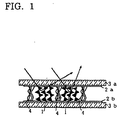
- FIG. 1 shows a simulated orientation diagram of liquid crystal display in which networks according to the invention are formed.
- FIG. 2(a) and FIG. 2(b) show optical microscopic photographs of a liquid crystal display in which networks according to the invention are formed.
- the plane shape of the networks may be of a polygon or of a shape surrounded by a closed curve as shown in the drawings. The shape does not matter.
- FIG. 3 shows a comparison, wherein an exemplary view (FIG. 3(a)) showing a liquid crystal display, in which networks according to the invention are formed, observed in the sectional direction, and its plan view (FIG. 3(b)) are compared with a sectional view (FIG. 3(c)) of a liquid crystal display, in which networks according to a prior art are formed, and its plan view (FIG. 3(d)).
- the section of the networks 4 according to the invention is pillar-like.
- the minimum diameter measured by vernier calipers of a liquid crystal layer means the diameter at which the vernier calipers are provided with the minimum width as shown in FIG. 4
- the maximum diameter measured by vernier calipers means the diameter at which the vernier calipers are provided with the maximum width as shown in FIG. 4.
- the contact area between liquid crystal and the polymer can be decreased in comparison with liquid crystal optical elements of a small network size described in the prior art. Accordingly, non-reacted monomer in the polymer is not eluted in liquid crystal and the reliability regarding the display performance can be improved.
- Schiff liquid crystal expressed by general formula (1) As liquid crystal used in the invention, Schiff liquid crystal expressed by general formula (1), azoxy-based liquid crystal expressed by general formula (2), cyanobiphenyl-based liquid crystal expressed by generation formula (3), cyanophenylester-based liquid crystal expressed by general formula (4), benzoic acid phenylester-based liquid crystal expressed by generation formula (5), cyclohexane carbonate phenylester based liquid crystal expressed by general formula (6), cyanophenyl cyclohexane based liquid crystal expressed by general formulas (7) and (8), pyrimidine-based liquid crystal expressed by general formulas (9) and (10), phenyldioxane-based liquid crystal expressed by general formula (11). tran-based liquid crystal expressed by general formula (12), and akenylcyclohexane benzonitrile based liquid crystal expressed by general formulas (1-3), (14) and (15) etc.. may be listed.
- n is an integral number 0 or 1.2.3,...
- R is an alkyl group, phenyl group, or cyclohexyl group and R' is an alkyl group, cyano group, or alkoxy group.
- 4-substitution 4'-substitution phenylester 4-(4-substitution cyclohexyl) benzoic acid 4'-substitution cyclohexylester, 4-substitution 4'-substitution biphenyl, 4-substitution phenyl 4'-substitution cyclohexane, 4-substitution 4"-substitution tarphenyl, 4-substitution biphenyl 4'-substitution cyclohexane.
- 2-(4-substitution phenyl)-5-substitution pyrimidine, cholesterol derivatives, etc.. may be listed.
- the invention is also featured in that, as a monomer used in the invention, a chemical compound, which is soluble with liquid crystal by heating although having interior solubility with liquid crystal at a normal temperature, is used.
- a chemical compound which is soluble with liquid crystal by heating although having interior solubility with liquid crystal at a normal temperature
- a chemical compound which is soluble with liquid crystal by heating although having interior solubility with liquid crystal at a normal temperature
- vinyl, etc. such as N-vinyl pyrrolidone, N-vinyl imidazole, vinyl sulfone, vinyl sulloxide, etc. may be used.
- diacrylate dibasic acid, dimethacrylate, and acrylate and methacrylate of their derivative bifuntional monomer, trifunctional monomer, or quadrifunctional monomer may be used. It is preferable that the monomer is a non-liquid crystal compound which can be completely separated from liquid crystal at normal temperature.
- the inventor et al. succeeded in forming networks whose size is large, by causing phase separation by slowly cooling from a state where monomer and liquid crystal are dissolved by heating. It was also confirmed that the size of the networks depends on the cooling speed. If the cooling speed is too slow, the liquid crystal becomes aggregate, and large polymer networks (domains) are formed. If the cooling speed is too fast, the liquid crystal is not sufficiently aggregated, wherein small networks are formed.
- phase separation between the monomer and liquid crystal After the phase separation between the monomer and liquid crystal is sufficiently completed, they are thermally hardened or completely made into macromolecules by irradiation of radiation rays such as ultraviolet rays. If they are heated or irradiated by radiation rays when the phase separation is insufficient, there is a possibility that the monomer remaining in liquid crystal forms minute networks. Therefore, it is important that the phase separation between the monomer and liquid crystal is sufficiently carried out. In this viewpoint, liquid crystal and monomer which have inferior solubility at normal temperature must be selected.
- the phase separation temperature between liquid crystal and monomer may be used as one of the indexes.
- a nematic liquid crystal layer is turned into an isotropic liquid layer, wherein the phase change temperature is called a phase transfer temperature (NI point).
- NI point phase transfer temperature
- monomer is likely to be solved with liquid crystal.
- phase separation occurs between the liquid crystal and monomer
- the solubility of monomer becomes, the more the phase separation temperature becomes lower than the Nl point. Therefore, it can be said that the smaller the difference between the Nl point and the phase separation temperature becomes, the more inferior the solubility becomes.
- the monomer used in the invention whose solubility with liquid crystal is not good at normal temperature, is used, it is hard to eiute the non-reacted monomer resultantly obtained in the liquid crystal display into liquid crystal, whereby it is possible to obtain a liquid crystal display having high reliability with respect to display performance (the reliability means a long-term stability of display performance in an environment when used, such as in particular, heat resistance, high temperature resistance, humidity resistance, etc.,)
- the speed of cooling down from a state, where monomer and liquid crystal are made soluble with each other by heating, to a temperature, at which phase separation occurs, or room temperature is 0.5°C through 10°C per minute, preferably, 1°C per minute. Also, it is confirmed by an optical microscope that the phase separation is completed, and the time when no change occurs in the networks is regarded as the time of completion of phase separation.
- Monomer used in the invention is used and blended with liquid crystal at a ratio of 0.1 through 20% by weight.
- a liquid crystal layer which is divided into comparatively large areas whose minimum diameter measured by vernier calipers is 5 ⁇ m and maximum diameter thereof is 100 ⁇ m.
- monomer having inferior solubility with liquid crystal is selected.
- a chiral agent Merck Corporation's brand names C15, ER-M, CB15, CM-22, CM-32, CM-34, CN, CM-21, CM-31, CM-33, CM-43L, S1011, R1011, S811, R811, and Asahi Denka's brand names CNL-611, CNL-617, etc.
- the chiral agent is doped so that the reflection wavelength of obtained liquid crystal display is in a range from 400 through 700nm, depending on the types thereof.
- a polymerization initiator of monomer it may be used.
- a polymerization initiator benzoilehtytether, 2-hydroxy-2-methyl-1-phenylpropane-1-on, 1-hydroxycyclo-hexylphenylketone, 2-methyl-1-(4-methyl-thio)phenyl)-2-morpholinopropanon-1, bisacylphosphine oxide, etc.
- benzoilehtytether 2-hydroxy-2-methyl-1-phenylpropane-1-on, 1-hydroxycyclo-hexylphenylketone, 2-methyl-1-(4-methyl-thio)phenyl)-2-morpholinopropanon-1, bisacylphosphine oxide, etc.
- One of these optical polymerization initiators or its combination may be used.
- Monomer is made into macromolecules by irradiating radiation rays such as ultraviolet rays, electron rays, rays, etc., at normal temperature.
- radiation rays such as ultraviolet rays, electron rays, rays, etc.
- a lamp of 40W through 160W is used, and irradiation is carried out for 30 seconds through 120 seconds.
- a liquid crystal layer which is divided into comparatively large areas whose minimum diameter measured by vernier calipers is 5 ⁇ m and maximum diameter measured by vernier calipers is 100 ⁇ m, is formed by polymer networks obtained by monomer whose solubility with liquid crystal is inferior at normal temperature, the PSCT has a high reflective index, and a liquid crystal display having an excellent quality of less visual angle dependency can be obtained. Furthermore, the liquid crystal display has a sufficient shock resistance properties, wherein it was confirmed that the reliability with respect to the display performance is high.
- the sectional shape of liquid crystal surrounded by the polymer networks is polygonal, generation of lump-like polymer networks, which do not contribute to display, is suppressed, the area occupied by liquid crystal contributing to the display is not decreased. Therefore, the display quality of a liquid crystal display which will be obtained can be improved.
- Brand name CB15 (Merck Corporation's 3-(2-methyl)propyl-3'-cyano-1-1'-biphenyl) is doped, at a ratio of 38% by weight, to Brand name Mixture PNM 108 (Dai-Nippon Ink, Inc.) in which diacryl monomer is mixed with nematic liquid crystal at a ratio of 20% by weight, and they are heated to 90°C, the sufficiently blended mixture is poured, in an atmosphere of 90°C, between two ITO (Indium Tin Oxide) 2a and 2b, and glass substrates 3a and 3b (See FIG. 1), which are spaced by spacers at intervals of 6.7 ⁇ m.
- ITO Indium Tin Oxide
- phase separation occurs between a liquid crystal layer and a monomer layer. After it is confirmed by an optical microscope that the phase separation has been sufficiently completed, it is optically hardened by irradiating a 80W high voltage mercury lamp for one minute.
- the diameter of respective twenty liquid crystal cells therein measured by vernier calipers was in a range from 5 through 50 ⁇ m as the minimum diameter, and was in a range from 10 through 100 ⁇ m as the maximum diameter.
- the optical dispersion is suppressed by the network structure of the obtained liquid crystal display, and the reflective index was 30% or so. No chromatic change occurred when diagonally observed the liquid crystal display.
- an Ohtsuka Denshi's LCD-7000 was used, wherein light having a wavelength of 580nm was irradiated on the display in a direction of 25 degrees with respect to the perpendicular line of the liquid crystal display, and a photomul (optical electron multiplier) in the front received the reflected light, wherein the spectral reflective index was measured.
- Brand name S101 (Merck Corporation's make) being a chiral agent is doped, at a ratio of 7.0% by weight, to Brand name Mixture PNM108 (Dai-Nippon Ink, Inc.) in which diacryl monomer is mixed with nematic liquid crystal at a ratio of 20% by weight and they are heated to 90°C.
- the sufficiently blended mixture is poured, in an atmosphere of 90°C, between two ITO 2a and 2b, and glass substrates 3a and 3b, which are spaced by spacers at intervals of 6.7 ⁇ m.
- phase separation occurs between a liquid crystal layer and a monomer layer. After the phase separation was sufficiency completed, it was optically hardened by irradiating a 80W high voltage mercury lamp for one minute.
- the diameter of respective twenty liquid crystal cells therein measured by vernier calipers was in a range from 10 through 45 ⁇ m as the minimum diameter, and was in a range from 15 through 100 ⁇ m as the maximum diameter.
- the optical dispersion is suppressed by the network structure of the obtained liquid crystal display, and the reflective index was 30% or so when having measured the reflective index by using light having a wavelength of 580nm by the method similar to that of the embodiment 1. No chromatic change occurred when diagonally observing the liquid crystal display.
- Nematic liquid crystal E44 (Brand name of Merck Corporation's cyanobiphenyl based liquid crystal) of 58.94% by weight, Brand name CB15 (Merck Corporation's make) being a chiral agent at 38% by weight, Brand name SL3435 -(Asahi Denka's make) being monomer of 3% by weight, and benzoin methylether of 0.06% by weight are sufficiently blended at 50°C to produce a uniform mixture.
- the mixture was poured between two ITO glass substrates spaced by spacers at intervals of 6.7 ⁇ m, and was optically hardened by irradiating a 80W high voltage mercury lamp thereto at 25°C for one minute.
- Nematic liquid E44 (Merck Corporation's make) of 62% by weight, and a chiral agent CB15 (Merck Corporation's make) of 38% by weight are sufficiently blended to produce a uniform mixture.
- the mixture was poured between two ITO glass substrates which is spaced by spacers at intervals of 6.7 ⁇ m. No polymer network is observed in the obtained liquid crystal display because no monomer is doped thereon.
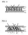
- the reflective index of the liquid crystal display was 35%, the reflection produced glare which is peculiar in the Bragg's reflection, wherein the reflected light changes, that is, green which is observed at the front side is turned into blue when the visual angle is changed. Also, by only slightly pressing the glass surface by a finger, the display completely disappears. At this time, it is considered that the liquid crystal particles are oriented as shown in FIG. 5.
Landscapes
- Physics & Mathematics (AREA)
- Nonlinear Science (AREA)
- Chemical & Material Sciences (AREA)
- Crystallography & Structural Chemistry (AREA)
- General Physics & Mathematics (AREA)
- Optics & Photonics (AREA)
- Liquid Crystal (AREA)
- Liquid Crystal Substances (AREA)
Claims (7)
- Eine Flüssigkristallanzeigevorrichtung, aufweisend eine Lichtmodulationsschicht, die zwischen zwei Substraten (3a, 3b) angeordnet ist, von denen mindestens eines transparent ist, wobei die Lichtmodulationsschicht ein Polymernetzwerk (4) und einen chiralen nematischen Flüssigkristall (1) aufweist, wobei das Polymernetzwerk durch Polymerisation eines Monomers geformt wird und den chiralen nematischen Flüssigkristall in Domänen teilt, die säulenartig und polygonal im Schnitt sind oder eine säulenartige Form haben, die von einer geschlossenen Kurve umschlossen wird, wobei der chirale nematische Flüssigkristall 90% oder mehr einer Fläche, die durch den Querschnitt der Lichtmodulationsschicht senkrecht zur Lichtmodulationsschichtnormalen definiert wird, belegt, dadurch gekennzeichnet, dass der minimale Durchmesser im Querschnitt von jeder der Domänen 5µm oder größer ist und der maximale Durchmesser im Querschnitt von jeder der Domänen 100µm oder kleiner ist, und dass kein verbleibendes Monomer in den Flüssigkristalldomänen übrig ist, um ein weiteres Polymernetzwerk in jeder der Domänen zu bilden.
- Eine Flüssigkristallanzeige nach Anspruch 1, wobei das Polymernetzwerk eine Wand bildet, die den chiralen nematischen Flüssigkristall in Domänen teilt, wobei die Wand eine einheitliche Dicke hat.
- Ein Verfahren zur Herstellung einer Flüssigkristallanzeigevorrichtung nach Anspruch 1 oder 2, wobei das Verfahren aufweist einen ersten Schritt des Erhitzens eines Monomers und eines chiralen nematischen Flüssigkristalls, um sie miteinander aufzulösen, einen zweiten Schritt des Anordnens des Monomers und des chiralen nematischen Flüssigkristalls zwischen zwei Substraten, einen dritten Schritt des Abkühlens der Lösung, was eine Phasenseparation zwischen dem Monomer und dem chiralen nematischen Flüssigkristall bewirkt, um ein Monomernetzwerk zu bilden, das den chiralen nematischen Flüssigkristall in Domänen teilt, und einen vierten Schritt des optischen Härtens des Monomemetzwerks durch Polymerisation, die durch Bestrahlung mit ultraviolettem Licht initialisiert wird, wodurch ein Polymernetzwerk gebildet wird, das den chiralen nematischen Flüssigkristall in Domänen teilt, wobei der minimale Durchmesser im Querschnitt von jeder 5µm oder größer ist und der maximale Durchmesser im Querschnitt von jeder 100µm oder kleiner ist, wobei die Phasenseparation während des Abkühlschrittes durch optische Mikroskopie kontrolliert wird, um zu vermeiden, dass Monomere in den Flüssigkristalldomänen verbleiben, um ein weiteres Polymernetzwerk in jeder der Domänen zu bilden, und wobei der Schritt des optischen Härtens erst ausgeführt wird, nachdem der Abkühlschritt beendet ist.
- Ein Verfahren nach Anspruch 3, wobei die Geschwindigkeit des Abkühlens von einer Temperatur, bei der das Monomer und der chirale nematische Flüssigkristall miteinander löslich sind, auf eine Temperatur, bei der Phasenseparation auftritt, oder auf Raumtemperatur im Bereich von 0,5°C bis 10°C pro Minute liegt.
- Ein Verfahren nach Anspruch 3 oder 4, wobei die Größe der Domänen von der Geschwindigkeit des Abkühlens abhängt.
- Ein Verfahren oder eine Auszeigevorrichtung nach einem der Ansprüche 1 bis 5, wobei der maximale Durchmesser im Querschnitt von den Domänen im Bereich von 10µm bis 100µm liegt.
- Ein Verfahren nach einem der Ansprüche 3 bis 5, wobei die Lösung aus einem Flüssigkristallmaterial mit der Strukturformel 3-(2-Methyl)propyl-3'-cyano-1-1'-biphenyl besteht, das in einem Verhältnis von 38 Gew.-% zu einer Mischung dotiert wird, in der ein Diacryl-Monomer mit einem nematischen Flüssigkristall in einem Verhältnis von 20 Gew.-% gemischt wird, und wobei die Lösung auf 90°C erhitzt wird und bei einer Temperatur von 90°C zwischen zwei ITO- (Indium Tin Oxide, Indiumzinnoxid) Elektroden, die auf den Substraten, die aus Glas gefertigt sind, angeordnet sind, gegossen wird und wobei die Lösung anschließend in 15 Minuten auf Raumtemperatur abgekühlt wird, wodurch Phasenseparation zwischen dem Flüssigkristallmaterial und dem Monomer eingeleitet wird, und wobei der Schritt des optischen Härtens ausgeführt wird durch Beleuchten der phasenseparierten Lösung mit einer 80W-Hochspannungsquecksilberlampe bei 25°C für eine Minute, wobei das Verfahren einen minimalen Durchmesser im Querschnitt von jeder der Domänen im Bereich von 5µm bis 50µm und einen maximalen Durchmesser im Querschnitt von jeder der Domänen in einem Bereich von 10µm bis 100µm bewirkt.
Applications Claiming Priority (2)
| Application Number | Priority Date | Filing Date | Title |
|---|---|---|---|
| JP27275399 | 1999-09-27 | ||
| JP27275399A JP2001091930A (ja) | 1999-09-27 | 1999-09-27 | 液晶表示体とその製造方法 |
Publications (3)
| Publication Number | Publication Date |
|---|---|
| EP1087253A2 EP1087253A2 (de) | 2001-03-28 |
| EP1087253A3 EP1087253A3 (de) | 2003-10-29 |
| EP1087253B1 true EP1087253B1 (de) | 2006-03-15 |
Family
ID=17518284
Family Applications (1)
| Application Number | Title | Priority Date | Filing Date |
|---|---|---|---|
| EP00307481A Expired - Lifetime EP1087253B1 (de) | 1999-09-27 | 2000-08-31 | Flüssigkristallvorrichtung und Verfahren zu deren Herstellung |
Country Status (6)
| Country | Link |
|---|---|
| US (1) | US6452651B1 (de) |
| EP (1) | EP1087253B1 (de) |
| JP (1) | JP2001091930A (de) |
| CN (1) | CN1155852C (de) |
| DE (1) | DE60026669T2 (de) |
| MY (1) | MY125510A (de) |
Families Citing this family (19)
| Publication number | Priority date | Publication date | Assignee | Title |
|---|---|---|---|---|
| KR100641631B1 (ko) * | 2000-02-01 | 2006-11-02 | 엘지.필립스 엘시디 주식회사 | 쌍안정 액정 셀 및 그 제조방법 |
| KR20020010211A (ko) * | 2000-07-27 | 2002-02-04 | 윤종용 | 액정 표시 장치 및 그의 제조 방법 |
| US6897915B1 (en) * | 2000-09-27 | 2005-05-24 | Kent State University | Non-lithographic photo-induced patterning of polymers from liquid crystal solvents with spatially modulated director fields |
| JP2002107768A (ja) * | 2000-09-29 | 2002-04-10 | Minolta Co Ltd | 液晶表示素子 |
| JP2002363564A (ja) * | 2001-06-01 | 2002-12-18 | Minolta Co Ltd | 液晶組成物及び反射型液晶表示素子 |
| US6853412B2 (en) | 2002-02-28 | 2005-02-08 | Eastman Kodak Company | Transaction card with memory and polymer dispersed cholesteric liquid crystal display |
| DE102004060835B4 (de) * | 2003-12-19 | 2015-02-26 | Asahi Glass Co., Ltd. | Optisches Flüssigkristallelement und Verfahren zu dessen Herstellung |
| JP4756313B2 (ja) * | 2003-12-19 | 2011-08-24 | 旭硝子株式会社 | 液晶光学素子及びその製造方法 |
| US7733448B2 (en) | 2004-10-29 | 2010-06-08 | Semiconductor Energy Laboratory Co., Ltd. | Liquid crystal display device |
| CN100410738C (zh) * | 2005-06-10 | 2008-08-13 | 奇美电子股份有限公司 | 液晶显示器的制造方法 |
| TWI331688B (en) | 2005-11-11 | 2010-10-11 | Ind Tech Res Inst | Reflective liquid crystal display assembly |
| US8570460B2 (en) * | 2005-12-19 | 2013-10-29 | Kent State University | Electronically-controllable polarization independent liquid crystal optical medium and devices using same |
| US8294850B2 (en) * | 2009-03-31 | 2012-10-23 | Apple Inc. | LCD panel having improved response |
| KR101574171B1 (ko) | 2009-12-08 | 2015-12-03 | 삼성전자주식회사 | 고분자 분산형 액정 디스플레이 장치 및 제조방법 |
| CN104090409A (zh) * | 2014-06-28 | 2014-10-08 | 中能柔性光电(滁州)有限公司 | 胆甾相柔性液晶显示装置及其制备方法 |
| CN109884834B (zh) * | 2019-04-24 | 2022-07-05 | 中国科学院宁波材料技术与工程研究所 | 一种液晶显示装置,制备方法及其使用方法 |
| CN110669530B (zh) * | 2019-10-15 | 2021-12-03 | 重庆汉朗精工科技有限公司 | 聚合物稳定液晶组合物的电控光学衍射元件及其制造方法 |
| CN111158179B (zh) * | 2019-12-30 | 2021-05-07 | 浙江大学 | 一种基于椭球状胆甾相液晶微液滴的温控调光膜及其状态转变方法 |
| PL445711A1 (pl) * | 2023-07-30 | 2025-02-03 | Uniwersytet Warszawski | Sposób kontroli domen związków organicznych wykazujących chiralność konformacyjną |
Family Cites Families (8)
| Publication number | Priority date | Publication date | Assignee | Title |
|---|---|---|---|---|
| US5490001A (en) * | 1990-11-19 | 1996-02-06 | Semiconductor Energy Laboratory Co., Ltd. | Ferroelectric liquid crystal device with an AC electric field producing a helical structure |
| US5847798A (en) * | 1991-05-02 | 1998-12-08 | Kent State University | Polymer stabilized black-white cholesteric reflective display |
| DE69229003T2 (de) | 1992-05-18 | 1999-10-21 | Kent State University, Kent | Flüssigkristalline, lichtmodulierende vorrichtung und material |
| EP0640863B1 (de) * | 1993-08-25 | 2002-11-13 | Matsushita Electric Industrial Co., Ltd. | Flüssigkristall-Anzeigevorrichtung |
| JP3259946B2 (ja) * | 1996-03-26 | 2002-02-25 | シャープ株式会社 | 液晶表示素子およびその製造方法 |
| US6061107A (en) * | 1996-05-10 | 2000-05-09 | Kent State University | Bistable polymer dispersed cholesteric liquid crystal displays |
| CN1155851C (zh) * | 1997-03-10 | 2004-06-30 | 佳能株式会社 | 液晶显示装置,应用此装置的投影仪及此装置的制作方法 |
| JPH10307288A (ja) * | 1997-05-09 | 1998-11-17 | Minolta Co Ltd | 液晶素子及びその製造方法 |
-
1999
- 1999-09-27 JP JP27275399A patent/JP2001091930A/ja active Pending
-
2000
- 2000-08-31 EP EP00307481A patent/EP1087253B1/de not_active Expired - Lifetime
- 2000-08-31 DE DE60026669T patent/DE60026669T2/de not_active Expired - Lifetime
- 2000-09-14 US US09/662,419 patent/US6452651B1/en not_active Expired - Fee Related
- 2000-09-25 MY MYPI20004461A patent/MY125510A/en unknown
- 2000-09-25 CN CNB00128794XA patent/CN1155852C/zh not_active Expired - Fee Related
Also Published As
| Publication number | Publication date |
|---|---|
| DE60026669T2 (de) | 2006-12-14 |
| MY125510A (en) | 2006-08-30 |
| EP1087253A3 (de) | 2003-10-29 |
| HK1035038A1 (en) | 2001-11-09 |
| DE60026669D1 (de) | 2006-05-11 |
| US6452651B1 (en) | 2002-09-17 |
| JP2001091930A (ja) | 2001-04-06 |
| CN1289943A (zh) | 2001-04-04 |
| CN1155852C (zh) | 2004-06-30 |
| EP1087253A2 (de) | 2001-03-28 |
Similar Documents
| Publication | Publication Date | Title |
|---|---|---|
| US6452651B1 (en) | Liquid crystal display and method for producing the same | |
| Lee et al. | Color-tunable mirrors based on electrically regulated bandwidth broadening in polymer-stabilized cholesteric liquid crystals | |
| EP0590984B1 (de) | Polymer dispergierter Flüssigkristallfilm, Flüssigkristallanzeige und Verfahren zur Herstellung | |
| JP4138759B2 (ja) | 液晶表示装置および電子機器 | |
| JP5761244B2 (ja) | 液晶組成物 | |
| Sharma et al. | Preparation and electrooptic study of reverse mode polymer dispersed liquid crystal: Performance augmentation with the doping of nanoparticles and dichroic dye | |
| EP0563403B1 (de) | Anzeigeelement und sein herstellungsverfahren | |
| KR100255624B1 (ko) | 페이퍼 화이트 pdlc 시스템 | |
| US20080106689A1 (en) | Display Element And Display Device | |
| EP0516076A2 (de) | Flüssigkristallvorrichtung | |
| JP2011090278A (ja) | 液晶表示装置 | |
| JP2016539374A (ja) | 透明薄肉フィルム、フィルムを製造するための方法、及び空間位相変調器 | |
| US6130738A (en) | Liquid crystal device having a resin wall using different resins with different surface interactions structure and manufacturing method for same | |
| US20160085095A1 (en) | Polymer-dispersed blue-phase liquid crystal films | |
| JP2003140183A (ja) | 反射型液晶表示装置 | |
| EP2322978A1 (de) | Reflektierende flüssigkristallanzeigevorrichtung | |
| Yang | Review of operating principle and performance of polarizer‐free reflective liquid‐crystal displays | |
| KR0162271B1 (ko) | 액정표시소자 및 그 제조방법 | |
| JP4393917B2 (ja) | 表示素子 | |
| JP3362711B2 (ja) | 液晶高分子層の製造方法および表示素子の製造方法 | |
| JPH10260388A (ja) | 反射型液晶表示素子及びその駆動方法 | |
| JPH08190086A (ja) | 液晶表示素子及びこれを用いた表示装置 | |
| JP5594662B2 (ja) | 表示素子、表示素子の製造方法 | |
| HK1035038B (en) | Liquid crystal display and method for producing the same | |
| JPH08134454A (ja) | 液晶表示素子及びこれを用いた表示装置 |
Legal Events
| Date | Code | Title | Description |
|---|---|---|---|
| PUAI | Public reference made under article 153(3) epc to a published international application that has entered the european phase |
Free format text: ORIGINAL CODE: 0009012 |
|
| 17P | Request for examination filed |
Effective date: 20000911 |
|
| AK | Designated contracting states |
Kind code of ref document: A2 Designated state(s): AT BE CH CY DE DK ES FI FR GB GR IE IT LI LU MC NL PT SE |
|
| AX | Request for extension of the european patent |
Free format text: AL;LT;LV;MK;RO;SI |
|
| PUAL | Search report despatched |
Free format text: ORIGINAL CODE: 0009013 |
|
| AK | Designated contracting states |
Kind code of ref document: A3 Designated state(s): AT BE CH CY DE DK ES FI FR GB GR IE IT LI LU MC NL PT SE |
|
| AX | Request for extension of the european patent |
Extension state: AL LT LV MK RO SI |
|
| 17Q | First examination report despatched |
Effective date: 20040312 |
|
| AKX | Designation fees paid |
Designated state(s): DE FR GB |
|
| GRAP | Despatch of communication of intention to grant a patent |
Free format text: ORIGINAL CODE: EPIDOSNIGR1 |
|
| GRAS | Grant fee paid |
Free format text: ORIGINAL CODE: EPIDOSNIGR3 |
|
| GRAA | (expected) grant |
Free format text: ORIGINAL CODE: 0009210 |
|
| AK | Designated contracting states |
Kind code of ref document: B1 Designated state(s): DE FR GB |
|
| REG | Reference to a national code |
Ref country code: GB Ref legal event code: FG4D |
|
| REF | Corresponds to: |
Ref document number: 60026669 Country of ref document: DE Date of ref document: 20060511 Kind code of ref document: P |
|
| ET | Fr: translation filed | ||
| PLBE | No opposition filed within time limit |
Free format text: ORIGINAL CODE: 0009261 |
|
| STAA | Information on the status of an ep patent application or granted ep patent |
Free format text: STATUS: NO OPPOSITION FILED WITHIN TIME LIMIT |
|
| 26N | No opposition filed |
Effective date: 20061218 |
|
| PGFP | Annual fee paid to national office [announced via postgrant information from national office to epo] |
Ref country code: DE Payment date: 20110824 Year of fee payment: 12 Ref country code: GB Payment date: 20110831 Year of fee payment: 12 Ref country code: FR Payment date: 20110818 Year of fee payment: 12 |
|
| GBPC | Gb: european patent ceased through non-payment of renewal fee |
Effective date: 20120831 |
|
| REG | Reference to a national code |
Ref country code: FR Ref legal event code: ST Effective date: 20130430 |
|
| PG25 | Lapsed in a contracting state [announced via postgrant information from national office to epo] |
Ref country code: DE Free format text: LAPSE BECAUSE OF NON-PAYMENT OF DUE FEES Effective date: 20130301 Ref country code: GB Free format text: LAPSE BECAUSE OF NON-PAYMENT OF DUE FEES Effective date: 20120831 |
|
| PG25 | Lapsed in a contracting state [announced via postgrant information from national office to epo] |
Ref country code: FR Free format text: LAPSE BECAUSE OF NON-PAYMENT OF DUE FEES Effective date: 20120831 |
|
| REG | Reference to a national code |
Ref country code: DE Ref legal event code: R119 Ref document number: 60026669 Country of ref document: DE Effective date: 20130301 |