EP1087039B9 - Wafer plating jig - Google Patents
Wafer plating jig Download PDFInfo
- Publication number
- EP1087039B9 EP1087039B9 EP99900165A EP99900165A EP1087039B9 EP 1087039 B9 EP1087039 B9 EP 1087039B9 EP 99900165 A EP99900165 A EP 99900165A EP 99900165 A EP99900165 A EP 99900165A EP 1087039 B9 EP1087039 B9 EP 1087039B9
- Authority
- EP
- European Patent Office
- Prior art keywords
- wafer
- conducting
- jig
- gripping
- plating jig
- Prior art date
- Legal status (The legal status is an assumption and is not a legal conclusion. Google has not performed a legal analysis and makes no representation as to the accuracy of the status listed.)
- Expired - Lifetime
Links
Images


Classifications
-
- C—CHEMISTRY; METALLURGY
- C25—ELECTROLYTIC OR ELECTROPHORETIC PROCESSES; APPARATUS THEREFOR
- C25D—PROCESSES FOR THE ELECTROLYTIC OR ELECTROPHORETIC PRODUCTION OF COATINGS; ELECTROFORMING; APPARATUS THEREFOR
- C25D17/00—Constructional parts, or assemblies thereof, of cells for electrolytic coating
- C25D17/06—Suspending or supporting devices for articles to be coated
- C25D17/08—Supporting racks, i.e. not for suspending
-
- H—ELECTRICITY
- H10—SEMICONDUCTOR DEVICES; ELECTRIC SOLID-STATE DEVICES NOT OTHERWISE PROVIDED FOR
- H10P—GENERIC PROCESSES OR APPARATUS FOR THE MANUFACTURE OR TREATMENT OF DEVICES COVERED BY CLASS H10
- H10P72/00—Handling or holding of wafers, substrates or devices during manufacture or treatment thereof
- H10P72/50—Handling or holding of wafers, substrates or devices during manufacture or treatment thereof for positioning, orientation or alignment
-
- C—CHEMISTRY; METALLURGY
- C25—ELECTROLYTIC OR ELECTROPHORETIC PROCESSES; APPARATUS THEREFOR
- C25D—PROCESSES FOR THE ELECTROLYTIC OR ELECTROPHORETIC PRODUCTION OF COATINGS; ELECTROFORMING; APPARATUS THEREFOR
- C25D17/00—Constructional parts, or assemblies thereof, of cells for electrolytic coating
- C25D17/001—Apparatus specially adapted for electrolytic coating of wafers, e.g. semiconductors or solar cells
-
- C—CHEMISTRY; METALLURGY
- C25—ELECTROLYTIC OR ELECTROPHORETIC PROCESSES; APPARATUS THEREFOR
- C25D—PROCESSES FOR THE ELECTROLYTIC OR ELECTROPHORETIC PRODUCTION OF COATINGS; ELECTROFORMING; APPARATUS THEREFOR
- C25D17/00—Constructional parts, or assemblies thereof, of cells for electrolytic coating
- C25D17/005—Contacting devices
-
- C—CHEMISTRY; METALLURGY
- C25—ELECTROLYTIC OR ELECTROPHORETIC PROCESSES; APPARATUS THEREFOR
- C25D—PROCESSES FOR THE ELECTROLYTIC OR ELECTROPHORETIC PRODUCTION OF COATINGS; ELECTROFORMING; APPARATUS THEREFOR
- C25D17/00—Constructional parts, or assemblies thereof, of cells for electrolytic coating
- C25D17/06—Suspending or supporting devices for articles to be coated
Definitions
- the present invention relates to a wafer plating jig in which a semiconductor wafer is mounted during a plating process.
- Fig. 1 shows the general construction of a wafer plating apparatus.
- the wafer plating apparatus is provided with a plating bath 1 accommodating a plating solution Q, a plating jig 2 disposed in the plating solution Q accommodated in the plating bath 1, a wafer 3 mounted in the plating jig 2, an anode 4 also disposed in the plating solution Q opposite the wafer 3, and a power source 5 connected between the plating jig 2 and the anode 4 for supplying an electrical current from the anode 4 to the plating jig 2 in order to form a plating film on the surface of the wafer 3.
- a collecting vessel 6 is provided around the outside of the plating bath 1 to collect plating solution Q that overflows from the plating bath 1.
- a circulating pump 7 is provided to circulate plating solution Q collected in the collecting vessel 6 back to the plating bath 1, supplying the plating solution Q into the bottom of the plating bath 1.
- a plurality of conducting pins are provided on the plating jig 2 for contacting the conductive layer formed on the surface of the wafer 3 mounted in the plating jig 2.
- a plating layer is formed on the surface of the wafer 3 by supplying an electrical current from the anode 4 to the conductive film on the wafer 3 via the conducting pins.
- an electrical current flows through the conducting pins when plating the wafer 3.
- plating matter since plating matter also becomes deposited on the ends of the conducting pins, it is occasionally necessary to perform a process to remove these deposits from the pins.
- the conducting pins are sealed from the plating solution Q in order to prevent plating matter from depositing on the ends of the conducting pins.
- no conventional wafer plating apparatus with a simple construction has included a seal construction capable of completely sealing individual conducting pins from the plating solution Q.
- a wafer plating jig comprising: a main jig body having a plate shape, an opening being formed in the center thereof; and a plurality of gripping mechanisms and a plurality of conducting pins disposed around a periphery of the opening for gripping the wafer and conducting electricity to the same; said gripping mechanism comprising: a base support; a holder rotatably fixed on a hinge pin supported on the base support; a coil spring for urging the front end of the holder toward a surface of the main jig body for gripping the wafer; a conducting pin positioned in the base support opposite the front end of the holder, said conducting pin being covered by a seal packing; wherein the wafer is gripped in the gripping mechanisms between the front ends of the holders and the conducting pins.
- a wafer plating jig as claimed in Claim 1 wherein the seal packing is formed by molding surrounding the conducting pin and has a bell-shaped, and end of the bell-shaped seal packing is protruding a prescribed length past the end of the conducting pin.
- a wafer plating jig as claimed in Claim 1, wherein: the gripping mechanism is provided with a cylinder formed of resin, which is inserted between the hinge pin and the coil spring.
- a wafer plating jig as claimed in Claim 1, wherein the wafer plating jig is provided with an open/close jig for connecting the rear ends of the holders of the gripping mechanisms commonly, so that the plural of gripping mechanisms is simultaneously opened or closed thereby.
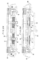
- Fig. 2A and 2B shows a plan view and cross-sectional view of the wafer plating jig according to the preferred embodiment.
- the wafer plating jig 10 is provided with a plate-shaped main body 11, a circular opening 12 formed in the center of the main body 11, and a plurality (eight, in the current example) of gripping mechanisms 13 mounted around the circumference of the circular opening 12 for gripping a wafer W.
- Figs. 3A-3D shows a plan view, side view, rear view, and cross-sectional view showing the construction of the gripping mechanisms 13.
- Each gripping mechanism 13 is provided with a base 14 having a supporting portion 14a on both ends, a hinge pin 15, a holder 16, and a coil spring 17.
- the hinge pin 15 is supported between the two supporting portions 14a,14a.
- the holder 16 is rotatably supported on the hinge pin 15.
- the holder 16 has a front end 16a and a back end 16b.
- the coil spring 17 provided around the hinge pin 15 urges the front end 16a of the holder 16 toward the bottom of the base 14 (see arrow B in Fig. 3B ).
- the base 14 is fixed to the main body 11 by screws 18,18.
- a cylindrical resinous sleeve 19 is interposed between the coil spring 17 and hinge pin 15. Accordingly, the position of the coil spring 17 around the hinge pin 15 is maintained by the resinous sleeve 19, thereby improving the stability of the rotating force that is generated by the urging force of the coil spring 17.
- a conducting pin 21 shown in Figs. 4A and 4B having an enlarged diameter portion 21a is disposed in a position opposing the front end 16a of the holder 16.
- a seal packing 20 formed of silicone rubber, fluoro rubber, or the like is molded to cover the conducting pin 21 and fit around the enlarged diameter portion 21a of the conducting pin 21.
- a bell-shaped protruding end of the seal packing 20 protrudes a prescribed dimension t over the ends of the conducting pin 21.
- Figs. 4A and 4B show a plan view and cross-sectional view respectively of the seal packing 20 and conducting pin 21.
- the holder 16 By pressing down on the back end 16b of the holder 16, the holder 16 resists the urging force of the coil spring 17 and opens by rotating around the hinge pin 15. When the back end 16b is released, the urging force of the coil spring 17 causes the holder 16 to rotate back in the opposite direction around the hinge pin 15 until closed.
- a wafer W is interposed between and gripped by the end of the conducting pin 21 and front end 16a of the holder 16, as shown in Fig. 3B , the end of the conducting pin 21 contacts the conductive film formed on the surface of the wafer W.
- the cylindrically shaped protruding end of the seal packing 20 contacts the surface of the wafer W.
- the seal packing 20 completely seals in the conducting pin 21, preventing plating solution from contacting the same.
- the protruding end of the seal packing 20 is capable of forming a close contact with the surface of the wafer W, thereby producing a sealing effect.
- an open/close jig 22 is provided to push on each of the back ends 16b of the holders 16 for opening/closing all of gripping mechanism 13 simultaneously, as shown in Fig. 5A .
- the open/close jig 22 pushes upward on the bottom of the back end 16b of the holder 16.
- a jig 23 transfers the wafer W to a position near the ends of the plurality of conducting pin 21, as shown in Fig. 5B . From this position, the open/close jig 22 is lowered to position the wafer W automatically by closing the gripping mechanisms.
- the surface of the holder 16 opposing the ends of the wafer W is configured to push the wafer W in a direction toward the center of the circular opening 12 as the holder 16 rotates about the hinge pin 15. Hence, by simultaneously rotating the plurality of holder 16 in the closing direction, the wafer W is automatically locked into a position. At this time, the wafer W is gripped between the front ends 16a of the holders 16 and the ends of the conducting pins 21.
- the seal packing 20 is formed by molding into a cylindrical shape to fit around the periphery of the conducting pin 21. Moreover, since the protruding end of the seal packing 20 is formed in a bell shape, when the seal packing 20 contacts the surface of the wafer W, the seal formed thereby has a small surface area. Accordingly, it is possible to form a tight seal with only a small amount of pushing force. Hence, each of the conducting pins 21 is completely sealed inside the seal packing 20. Further, since the seal packing 20 is formed by molding to fit around the conducting pin 21, the positional relationship between the ends of the conducting pin 21 and the ends of the seal packing 20 are fixed (the dimension t shown in Fig. 4B is fixed), thereby achieving a stable seal.
- the circular opening 12 is formed in the plate-shaped main body 11.
- the circular opening 12 is not limited to a circular shape but can also have a rectangular shape, for example.
- Figs. 6A and 6B show a plating jig 10 having a rectangular opening 12 and a plurality of gripping mechanisms 13 disposed around the peripheral edge of the opening.
- Various electronic components may also be mounted in the area D of the plating jig 10 shown in Fig. 2 , such as a component provided to supply electricity to the wafer W via the conducting pins 21.
- these electronic components are not directly related to the present invention, a description of them has been omitted.
- the present invention is appropriate for use in an apparatus, which is used to plate a semiconductor wafer or the like.
Landscapes
- Chemical & Material Sciences (AREA)
- Engineering & Computer Science (AREA)
- Chemical Kinetics & Catalysis (AREA)
- Electrochemistry (AREA)
- Materials Engineering (AREA)
- Metallurgy (AREA)
- Organic Chemistry (AREA)
- Life Sciences & Earth Sciences (AREA)
- Sustainable Development (AREA)
- Electroplating Methods And Accessories (AREA)
- Electrodes Of Semiconductors (AREA)
- Container, Conveyance, Adherence, Positioning, Of Wafer (AREA)
Applications Claiming Priority (3)
| Application Number | Priority Date | Filing Date | Title |
|---|---|---|---|
| JP10018151A JPH11204460A (ja) | 1998-01-12 | 1998-01-12 | ウエハのメッキ治具 |
| JP1815198 | 1998-01-12 | ||
| PCT/JP1999/000059 WO1999035309A1 (fr) | 1998-01-12 | 1999-01-12 | Support pour metallisation de tranches |
Publications (4)
| Publication Number | Publication Date |
|---|---|
| EP1087039A1 EP1087039A1 (en) | 2001-03-28 |
| EP1087039A4 EP1087039A4 (en) | 2006-05-31 |
| EP1087039B1 EP1087039B1 (en) | 2008-10-29 |
| EP1087039B9 true EP1087039B9 (en) | 2009-08-19 |
Family
ID=11963625
Family Applications (1)
| Application Number | Title | Priority Date | Filing Date |
|---|---|---|---|
| EP99900165A Expired - Lifetime EP1087039B9 (en) | 1998-01-12 | 1999-01-12 | Wafer plating jig |
Country Status (6)
| Country | Link |
|---|---|
| US (1) | US6365020B1 (https=) |
| EP (1) | EP1087039B9 (https=) |
| JP (1) | JPH11204460A (https=) |
| KR (1) | KR100586473B1 (https=) |
| DE (1) | DE69939827D1 (https=) |
| WO (1) | WO1999035309A1 (https=) |
Families Citing this family (15)
| Publication number | Priority date | Publication date | Assignee | Title |
|---|---|---|---|---|
| US6248222B1 (en) * | 1998-09-08 | 2001-06-19 | Acm Research, Inc. | Methods and apparatus for holding and positioning semiconductor workpieces during electropolishing and/or electroplating of the workpieces |
| TWI228548B (en) * | 2000-05-26 | 2005-03-01 | Ebara Corp | Apparatus for processing substrate and apparatus for processing treatment surface of substrate |
| US20040007460A1 (en) * | 2002-07-15 | 2004-01-15 | Karl Sagedahl | Clamping device having barbed pin |
| US20050145486A1 (en) * | 2004-01-07 | 2005-07-07 | Chung-Ho Chen | Clipping device of an electroplating base plate |
| US20050274604A1 (en) * | 2004-02-06 | 2005-12-15 | Koji Saito | Plating apparatus |
| USD583779S1 (en) | 2006-07-13 | 2008-12-30 | Ebara Corporation | Electrolytic plating anode |
| USD572673S1 (en) | 2006-07-13 | 2008-07-08 | Ebara Corporation | Anode shaft |
| US7507319B2 (en) * | 2006-07-21 | 2009-03-24 | Ebara Corporation | Anode holder |
| US9464362B2 (en) | 2012-07-18 | 2016-10-11 | Deca Technologies Inc. | Magnetically sealed wafer plating jig system and method |
| US8932443B2 (en) | 2011-06-07 | 2015-01-13 | Deca Technologies Inc. | Adjustable wafer plating shield and method |
| JP6247557B2 (ja) * | 2014-02-14 | 2017-12-13 | 株式会社Jcu | 基板めっき治具 |
| KR101647074B1 (ko) | 2016-06-07 | 2016-08-09 | 정진호 | 사면 연동 로테이션에 기반을 둔 도금 지그 거치용 틸팅 승강 유도체 |
| JP6713863B2 (ja) * | 2016-07-13 | 2020-06-24 | 株式会社荏原製作所 | 基板ホルダ及びこれを用いためっき装置 |
| CN112251796A (zh) * | 2020-10-15 | 2021-01-22 | 中山市汇佳精密科技有限公司 | 应用于太阳能电池片电镀挂具上的可翻转框架 |
| CN119943672B (zh) * | 2025-01-03 | 2025-10-31 | 华天科技(西安)有限公司 | 一种单颗qfn框架类产品锡化的方法、治具 |
Family Cites Families (13)
| Publication number | Priority date | Publication date | Assignee | Title |
|---|---|---|---|---|
| US2739117A (en) * | 1952-06-18 | 1956-03-20 | Gen Motors Corp | Electroplating fixture |
| US3461059A (en) * | 1966-10-10 | 1969-08-12 | Hammond Machinery Builders Inc | Power operated electro-chemical fixture |
| DE3028635A1 (de) * | 1980-07-29 | 1982-03-04 | Degussa Ag, 6000 Frankfurt | Vorrichtung zum partiellen galvanischen beschichten |
| JPS61187379A (ja) | 1985-02-15 | 1986-08-21 | Sanyo Electric Co Ltd | 光起電力装置の製造方法 |
| JPS61187379U (https=) * | 1985-05-13 | 1986-11-21 | ||
| JPH0686676B2 (ja) | 1985-10-18 | 1994-11-02 | 旭化成工業株式会社 | メツキ用電極部 |
| JPS62188798A (ja) | 1986-02-14 | 1987-08-18 | Fujitsu Ltd | メツキ用コンタクトピン |
| FR2633452B1 (fr) * | 1988-06-28 | 1990-11-02 | Doue Julien | Dispositif de support pour un substrat mince, notamment en un materiau semiconducteur |
| US5135636A (en) * | 1990-10-12 | 1992-08-04 | Microelectronics And Computer Technology Corporation | Electroplating method |
| JPH05222587A (ja) | 1992-02-06 | 1993-08-31 | Ibiden Co Ltd | 電着塗装用クランプ |
| JPH0813198A (ja) | 1994-07-04 | 1996-01-16 | Hitachi Ltd | 接触導通用電極及びそれを用いた半導体製造装置 |
| US6228231B1 (en) * | 1997-05-29 | 2001-05-08 | International Business Machines Corporation | Electroplating workpiece fixture having liquid gap spacer |
| CH693133A5 (de) * | 1997-08-21 | 2003-03-14 | Mecatool Ag | Kupplungsanordnung für eine Bearbeitungseinrichtung. |
-
1998
- 1998-01-12 JP JP10018151A patent/JPH11204460A/ja active Pending
-
1999
- 1999-01-12 KR KR1020007007645A patent/KR100586473B1/ko not_active Expired - Lifetime
- 1999-01-12 EP EP99900165A patent/EP1087039B9/en not_active Expired - Lifetime
- 1999-01-12 DE DE69939827T patent/DE69939827D1/de not_active Expired - Lifetime
- 1999-01-12 WO PCT/JP1999/000059 patent/WO1999035309A1/ja not_active Ceased
- 1999-01-12 US US09/600,028 patent/US6365020B1/en not_active Expired - Lifetime
Also Published As
| Publication number | Publication date |
|---|---|
| WO1999035309A1 (fr) | 1999-07-15 |
| JPH11204460A (ja) | 1999-07-30 |
| EP1087039A4 (en) | 2006-05-31 |
| KR100586473B1 (ko) | 2006-06-07 |
| DE69939827D1 (de) | 2008-12-11 |
| EP1087039B1 (en) | 2008-10-29 |
| US6365020B1 (en) | 2002-04-02 |
| KR20010034038A (ko) | 2001-04-25 |
| EP1087039A1 (en) | 2001-03-28 |
Similar Documents
| Publication | Publication Date | Title |
|---|---|---|
| EP1087039B9 (en) | Wafer plating jig | |
| JP5886484B2 (ja) | 製品保持装置および処理方法 | |
| JP4669019B2 (ja) | 基板ホルダ及び電解めっき装置 | |
| EP0379289B1 (en) | Fixture and a method for plating contact bumps for integrated circuits | |
| US6849167B2 (en) | Electroplating reactor including back-side electrical contact apparatus | |
| CN104838047B (zh) | 磁性密封的晶片电镀夹具系统和方法 | |
| US20150090584A1 (en) | Plating apparatus and cleaning device used in the plating apparatus | |
| CN113825860B (zh) | 基板保持器及具备该基板保持器的基板镀覆装置、以及电接点 | |
| JPH11204460A5 (https=) | ||
| US20060070883A1 (en) | Fixtureless vertical paddle electroplating cell | |
| US10954603B2 (en) | Substrate holder, plating apparatus, plating method, and electric contact | |
| JP4037504B2 (ja) | 半導体ウエハのメッキ治具 | |
| TW512476B (en) | Substrate holder | |
| US6181057B1 (en) | Electrode assembly, cathode device and plating apparatus including an insulating member covering an internal circumferential edge of a cathode member | |
| EP1113093B1 (en) | Semiconductor wafer holder and electroplating system for plating a semiconductor wafer | |
| JP4044191B2 (ja) | ウエハのメッキ装置 | |
| JP2001006597A (ja) | 試料搭載装置 | |
| KR20200073997A (ko) | 기판 홀더에 사용하는 시일 | |
| KR100293238B1 (ko) | 기질 도금장치용 랙 | |
| JPH08165599A (ja) | セラミックパッケージの部分メッキ治具と部分メッキ方法 |
Legal Events
| Date | Code | Title | Description |
|---|---|---|---|
| PUAI | Public reference made under article 153(3) epc to a published international application that has entered the european phase |
Free format text: ORIGINAL CODE: 0009012 |
|
| 17P | Request for examination filed |
Effective date: 20000712 |
|
| AK | Designated contracting states |
Kind code of ref document: A1 Designated state(s): DE FR GB |
|
| A4 | Supplementary search report drawn up and despatched |
Effective date: 20060420 |
|
| GRAP | Despatch of communication of intention to grant a patent |
Free format text: ORIGINAL CODE: EPIDOSNIGR1 |
|
| GRAS | Grant fee paid |
Free format text: ORIGINAL CODE: EPIDOSNIGR3 |
|
| GRAA | (expected) grant |
Free format text: ORIGINAL CODE: 0009210 |
|
| AK | Designated contracting states |
Kind code of ref document: B1 Designated state(s): DE FR GB |
|
| REG | Reference to a national code |
Ref country code: GB Ref legal event code: FG4D |
|
| REF | Corresponds to: |
Ref document number: 69939827 Country of ref document: DE Date of ref document: 20081211 Kind code of ref document: P |
|
| PGFP | Annual fee paid to national office [announced via postgrant information from national office to epo] |
Ref country code: GB Payment date: 20090121 Year of fee payment: 11 |
|
| RTI2 | Title (correction) |
Free format text: WAFER PLATING JIG |
|
| PLBE | No opposition filed within time limit |
Free format text: ORIGINAL CODE: 0009261 |
|
| STAA | Information on the status of an ep patent application or granted ep patent |
Free format text: STATUS: NO OPPOSITION FILED WITHIN TIME LIMIT |
|
| 26N | No opposition filed |
Effective date: 20090730 |
|
| PGFP | Annual fee paid to national office [announced via postgrant information from national office to epo] |
Ref country code: FR Payment date: 20081230 Year of fee payment: 11 |
|
| GBPC | Gb: european patent ceased through non-payment of renewal fee |
Effective date: 20100112 |
|
| REG | Reference to a national code |
Ref country code: FR Ref legal event code: ST Effective date: 20100930 |
|
| PG25 | Lapsed in a contracting state [announced via postgrant information from national office to epo] |
Ref country code: FR Free format text: LAPSE BECAUSE OF NON-PAYMENT OF DUE FEES Effective date: 20100201 |
|
| PG25 | Lapsed in a contracting state [announced via postgrant information from national office to epo] |
Ref country code: GB Free format text: LAPSE BECAUSE OF NON-PAYMENT OF DUE FEES Effective date: 20100112 |
|
| PGFP | Annual fee paid to national office [announced via postgrant information from national office to epo] |
Ref country code: DE Payment date: 20180103 Year of fee payment: 20 |
|
| REG | Reference to a national code |
Ref country code: DE Ref legal event code: R071 Ref document number: 69939827 Country of ref document: DE |