EP1069574A2 - Résistance non linéaire en fonction de la tension et limiteur de surtension - Google Patents
Résistance non linéaire en fonction de la tension et limiteur de surtension Download PDFInfo
- Publication number
- EP1069574A2 EP1069574A2 EP00115336A EP00115336A EP1069574A2 EP 1069574 A2 EP1069574 A2 EP 1069574A2 EP 00115336 A EP00115336 A EP 00115336A EP 00115336 A EP00115336 A EP 00115336A EP 1069574 A2 EP1069574 A2 EP 1069574A2
- Authority
- EP
- European Patent Office
- Prior art keywords
- voltage non
- linear resistor
- metal fitting
- terminal metal
- linear
- Prior art date
- Legal status (The legal status is an assumption and is not a legal conclusion. Google has not performed a legal analysis and makes no representation as to the accuracy of the status listed.)
- Withdrawn
Links
Images


Classifications
-
- H—ELECTRICITY
- H01—ELECTRIC ELEMENTS
- H01C—RESISTORS
- H01C7/00—Non-adjustable resistors formed as one or more layers or coatings; Non-adjustable resistors made from powdered conducting material or powdered semi-conducting material with or without insulating material
- H01C7/10—Non-adjustable resistors formed as one or more layers or coatings; Non-adjustable resistors made from powdered conducting material or powdered semi-conducting material with or without insulating material voltage responsive, i.e. varistors
- H01C7/105—Varistor cores
- H01C7/108—Metal oxide
- H01C7/112—ZnO type
-
- H—ELECTRICITY
- H01—ELECTRIC ELEMENTS
- H01C—RESISTORS
- H01C7/00—Non-adjustable resistors formed as one or more layers or coatings; Non-adjustable resistors made from powdered conducting material or powdered semi-conducting material with or without insulating material
- H01C7/10—Non-adjustable resistors formed as one or more layers or coatings; Non-adjustable resistors made from powdered conducting material or powdered semi-conducting material with or without insulating material voltage responsive, i.e. varistors
- H01C7/12—Overvoltage protection resistors; Arresters
-
- B—PERFORMING OPERATIONS; TRANSPORTING
- B23—MACHINE TOOLS; METAL-WORKING NOT OTHERWISE PROVIDED FOR
- B23K—SOLDERING OR UNSOLDERING; WELDING; CLADDING OR PLATING BY SOLDERING OR WELDING; CUTTING BY APPLYING HEAT LOCALLY, e.g. FLAME CUTTING; WORKING BY LASER BEAM
- B23K35/00—Rods, electrodes, materials, or media, for use in soldering, welding, or cutting
- B23K35/22—Rods, electrodes, materials, or media, for use in soldering, welding, or cutting characterised by the composition or nature of the material
- B23K35/24—Selection of soldering or welding materials proper
- B23K35/26—Selection of soldering or welding materials proper with the principal constituent melting at less than 400°C
- B23K35/262—Sn as the principal constituent
Definitions
- the present invention relates to a voltage non-linear resistor unit and an arrester unit used for a power system equipment.
- a voltage non-linear resistor is used for an arrester used in an electric circuit which protects a power system from an abnormal voltage.
- a zinc oxide (ZnO)-based material which is a ceramic material, is used as a base element of the voltage non-linear resistor.
- a sintered body is used as the base element, which is prepared in the manner that, to the zinc oxide (ZnO) used as a main component, there are added an oxide such as bismuth (Bi), antimony (Sb), nickel (Ni), cobalt (Co), manganese (Mn), chromium (Cr), silicon (Si) or the like used as a secondary component, water and an organic binder added, and then, these components are sufficiently agitated. Thereafter, these components are granulated and molded by using a spray dryer or the like, and then, are sintered.
- a side of the sintered body is formed with a high resistance layer as occasion demands by applying and re-sintering a high resistance substance for preventing a creepage flash fault.
- Both ends of the sintered body are polished and are attached with an electrode film, and thus, a voltage non-linear resistor is manufactured.
- An arrester is constructed in a manner that one or plural voltage non-linear resistor elements are laminated or stacked, and then, are attached with a terminal metal fitting through an insulator.
- a spring structure is employed for electrically connecting the terminal metal fitting.
- a conductive paste consisting of silver powder, glass powder and an organic binder is used as a conductive material, and glass powder contributing to a bonding strength is an insulator.
- the thus formed junction surface is inferior in a conductivity, and therefore, a uniform conductivity is hard to be obtainable.
- the following problem has arisen. That is, a current concentration is easy to be generated in discharge withstand current rating, and then, the discharge withstand current rating is decreased.
- An object of the present invention is to provide a voltage non-linear resistor unit which can achieve a small size without lowering discharge withstand current rating.
- Another object of the present invention is to provide an arrester unit provided with the voltage non-linear resistor unit of the character mentioned above.
- a voltage non-linear resistor unit comprising:
- a shift between central axes of one and the other joint surfaces is within a range of 0.1 ⁇ R5 or less where R5 is a diameter of a smaller joint surface.
- the sintered body of the voltage non-linear resistor is provided with a side surface to which an inorganic insulation coating material, which is formed with a high resistance layer containing mullite (Al 6 Si 2 O 13 ) as a main component and including AlPO 4 of 5.0 to 20wt%, TiO 2 or Fe 2 O 3 of 0.2 to 5wt%, is preliminarily formed.
- a non-crystal high resistance layer including SiO 2 and Al 2 O 3 as main component is further formed on the inorganic insulating coating material.
- the electrode film formed on the sintered body is an electrode film composed of a plurality of layers comprising a first layer of Al or Al alloy and a second layer of Cu or Cu alloy.
- the electrode film has a thickness of 300 ⁇ m or less.
- the soldering material contains Sn as a main component and contains at least one of Cu, Ag and Sb as a secondary component such that Sn is contained by 70 to 99%, Ag is contained by 3 to 20%, and Cu and Sb are contained by 5% or less.
- an arrester unit comprising:
- the metallic disc includes a plurality of protrusions at a side facing the first-mentioned terminal metal fitting of the voltage non-linear resistor unit.
- the elastic insulating cover member is formed with a thin wall portion in one directional side.
- a clearance between the voltage non-linear resistors forming the electrode film and a clearance between both the end surfaces of the voltage non-linear resistor and the terminal metal fitting are joined by means of soldering material. Therefore, it is possible to provide a voltage non-linear resistor unit which has a compact size with reduced cost. Furthermore, since the bonding strength of the voltage non-linear resistors is high, it is possible to provide a voltage non-linear resistor unit with no peeling even if it receives an external force, an ambient temperature, and an internal heating effect.
- these voltage non-linear resistor units are fully joined in its structure, and in the manufacturing of an arrester unit, in the case of covering these voltage non-linear resistor units with the perforated insulating tube and the elastic insulating cover member, these members are not held between the joint interfaces. Therefore, it is possible to prevent a corona generated in a voltage application without losing an electrical characteristic.
- FIG. 1 is a view to explain a voltage non-linear resistor unit according to one embodiment of the present invention.
- a voltage nonlinear resistor unit 1 is capable of being mounted in a columnar (tubular) transformer and in a distributing board (switch board).
- the voltage non-linear resistor unit 1 is formed in a manner that one or plural voltage non-linear resistors 2 are laminated or stacked, and both end portions of the laminated voltage non-linear resistor 2 are attached with a projected terminal metal fitting 4 having a screw (threaded) portion.
- a soldering material 3 is interposed between the voltage non-linear resistors 2 and between the voltage non-linear resistor 2 and the terminal metal fitting 4.
- FIG. 1 there is shown a voltage non-linear resistor unit 1 which is formed by piling up five voltage non-linear resistors 2.
- Each of the voltage non-linear resistors 2 is formed in the following manner. That is, a raw material is prepared in a manner that ZnO is used as a main component, and a micro amount of additives such as Bi is weighed by a predetermined amount as a secondary component. Then, the raw material is mixed with water and an organic binder such as a dispersant by a mixer. Next, the mixture is sprayed and granulated by a spray dryer so as to have a predetermined grain size of, for example, 100 ⁇ m. Subsequently, the granulated powder is put into a mold to be pressurized, and then, is molded into a cylindrical shape, and thus, a compact is obtained.
- the compact thus obtained is sintered in the air at a temperature of, for example, 500 °C in order to remove an added organic binder or like, and further, is sintered in the air at a temperature of 1200 °C for two hours, thus obtaining a sintered body 5 as shown in FIG. 2.
- both end surfaces of the sintered body 5 are polished by using a grindstone having a surface roughness, in which an arithmetic average surface roughness (center line average surface roughness) Ra ranges from 1 to 2 ⁇ m, so as to form an electrode film surface.
- a silver paste 6 preliminarily prepared at predetermined blending is applied to both the end surfaces, and thus, a voltage non-linear resistor 2 having an electrode film layer is obtained.
- soldering material 3 is arranged on the surface of the voltage non-linear resistor 2 which is formed with the electrode film, and then, a predetermined number, for example, 5 (five) voltage non-linear resistors 2 are piled up, and further, the terminal metal fitting 4 having a predetermined shape is arranged on each of both end surfaces of the voltage non-linear resistors 2 thus piled up. Further, the soldering material 3 is melted in the manner shown in FIG. 3 and FIG. 4.
- a voltage non-linear resistor unit 1 is set so as to be supported by using a supporting base 7 and a supporting rod 8 in a state of contacting to the voltage non-linear resistor 2 at a portion different from a joint surface between the voltage non-linear resistors 2 and between the voltage non-linear resistor 2 and the terminal metal fitting 4. Then, a local portion of the joint portion, on which a soldering material 3 is arranged, is heated by abutting a heat source 9 thereagainst to apply a load to the joint portion in the vertical direction while giving a rotation.
- a temperature is increased up to the maximum at a temperature rising speed of 60°C /min, and then, the maximum temperature is increased up to 30 °C or more than a melting point of the soldering material 3. Thereafter, the temperature is decreased at a temperature rising speed of 10 °C /min, and thus, the voltage non-linear resistor unit 1 can be obtained.
- the voltage non-linear resistor unit 1 thus obtained has the same electrical characteristic as that in the case where five voltage non-linear resistors 2 are laminated via an insulator as in the conventional structure.
- a surface roughness of the sintered body 5 has been controlled by a grindstone.
- the surface roughness of the sintered body 5 may be subjected to a blasting working by using a powder having a predetermined grain size after being polished. In such a case, more uniform control can be performed.
- a porosity of the surface of the sintered body 5 is 15% or less, a strength of the base element is improved, and then, de-granulation is not caused in the grindstone polishing and blasting working, and therefore, it is possible to obtain a preferable bonding strength between the base element surface and the electrode film surface when forming an electrode film.
- a composition ratio for forming the voltage non-linear resistor 2 is selected in the following manner. That is, ZnO is used as a main component, bismuth, cobalt, manganese, antimony and nickel are reduced to Bi 2 O, Co 2 O 3 , Sb 2 O 3 and NiO, respectively, and then, Bi 2 O 3 is contained by 0.1 to 5mol%, Co 2 O 3 is contained by 0.1 to 5mol%, MnO is contained by 0.1 to 5mol%, Sb 2 O 3 is contained by 0.1 to 5mol%, and NiO is contained by 0.1 to 5mol%, respectively, and thus, a fundamental component is prepared.
- a sintered body 5 is manufactured on the basis of a composition ratio comprising a ratio of MnO/Sb 2 O 3 ranging from 0.3 to 1 and a ratio of Sb 2 O 3 /Bi 2 O 3 ranging from 1 to 7.
- the sintered body thus manufactured can reduce its porosity and improve the strength of base element. Therefore, the base element is hard to cause a de-granulation in the grindstone polishing and blasting working, and it is possible to obtain a preferable bonding strength between the surface on which the electrode film is formed and the electrode film surface.
- the voltage non-linear resistor 2 may be formed as shown in FIG. 5, in place of the voltage non-linear resistor 2 shown in FIG. 2. More specifically, an inorganic insulating coating material 10 consisting mainly of a low melting point glass is applied and baked onto a side of the sintered body 5, and then, both sides of the sintered body 5 are polished at a predetermined surface roughness so as to form an electrode film surface. Subsequently, a Cu electrode film 11 is formed by an arc spraying method by using an arc discharge in place of the silver paste 6, and thus, a voltage non-linear resistor 2 is obtained.
- an inorganic insulating coating material 10 consisting mainly of a low melting point glass is applied and baked onto a side of the sintered body 5, and then, both sides of the sintered body 5 are polished at a predetermined surface roughness so as to form an electrode film surface.
- a Cu electrode film 11 is formed by an arc spraying method by using an arc discharge in place of the silver paste 6, and thus,
- the voltage non-linear resistor 2 thus obtained is excellent in an insulating characteristic in discharge by the inorganic insulating coating material 10 applied onto the side of the sintered body 5, and thus, its withstand current rating is improved. Moreover, the Cu electrode film 11 is excellent in a conductivity and a heat radiation is suppressed in its discharge, so that a thermal stress given to the soldering material 3 can be suppressed.
- the Cu electrode film 11 has been formed by using an arc spraying method in place of the silver paste 6. Further, even if the Cu electrode film 11 is formed in the following methods, the same effect could be obtained. That is, the methods include: a plasma spraying method of using a Cu alloy, e.g., a Cu-Zn alloy as an electrode film material, melting the material by a plasma heat source so that an electrode film is formed on the surface of a base element; a high velocity gas flame spraying method of spraying a material melted by using a high velocity gas flame to the surface of the base element at a high velocity so as to form an electrode film; and a high velocity spraying method of spraying a material at a high velocity so that an electrode film is formed on the surface of a base element.
- a plasma spraying method of using a Cu alloy e.g., a Cu-Zn alloy as an electrode film material
- a high velocity gas flame spraying method of spraying a material melted by using a high velocity gas flame to the surface of
- a voltage non-linear resistor 2 as shown in FIG. 6 may be formed so as to improve the discharge withstand current rating characteristic and the bonding strength. More specifically, mullite is used as a main component of a side insulating coating material, and then, is baked at 400 °C after adding a predetermined amount of primary aluminum phosphate, TiO 2 or Fe 2 O 3 thereto. Further, the sintered body 5 is formed with a high resistance layer 12 containing AlPO 4 using mullite as a main component of 0 to 20wt%, and TiO 2 or Fe 2 O 3 of 0.2 to 5wt%, at the side thereof. Further, as occasion demands, a non-crystal high resistance layer 15 using SiO 2 and Al 2 O 3 as a main component is further formed on the high resistance layer 12.
- the sintered body 5 is polished at a predetermined surface roughness, and then, an Al or Al alloy layer is formed on the polished surface as a first electrode film 13, and further, a Cu or Cu alloy layer is formed on the polished surface as a second electrode film 14, and in this manner, the voltage non-linear resistor 2 is obtained.
- the boding strength with the sintered body 5 can be improved.
- the porosity of the side insulating coating material decreases, it is possible to provide the voltage non-linear resistor 2 which is excellent in the discharge withstand current rating.
- the high resistance layer 15 is formed, it is possible to provide the voltage non-linear resistor 2 which can improve a water repellence and is excellent in a moisture resistance characteristic.
- the first electrode film 13 aluminum or aluminum alloy having a low melting point and a low Young's modulus is used as the first electrode film 13, and then, is interposed between layers comprising Cu or Cu alloy which is the second electrode film 14. Therefore, it is possible to provide a voltage non-linear resistor 2 which has a more stable bonding strength.
- the bonding strength and discharge withstand current rating characteristics have been improved by using the voltage non-linear resistor 2 including a material for forming the electrode film and the insulating coating material.
- the state of forming the electrode film and the thickness of the electrode film give an influence to the discharge withstand current rating characteristic. Therefore, the voltage non-linear resistor unit including the electrode film having different thickness was previously manufactured by the voltage non-linear resistor 2 shown in FIG. 2, and then, a relationship with its discharge withstand current rating characteristic was investigated.
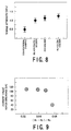
- FIG. 7 is a graph showing a relationship between the thickness of the electrode film and the discharge withstand current rating in this embodiment of the present invention.
- the abscissa takes a thickness of electrode film
- the ordinate takes a current value before breakage when energizing an impulse current, which is plotted.
- the discharge withstand current rating characteristic is greatly reduced.
- the voltage non-linear resistor 2 shown in FIG. 2 has been used. It was confirmed that the same effect can be obtained as in the case where the voltage non-linear resistor 2 shown in FIG. 5 and FIG. 6 is used.
- a tensile strength test was carried out. More specifically, a jig is attached to a tap provided on the terminal metal fitting 4, and then, a tensile strength was measured.
- a voltage non-linear resistor unit 1 was prepared in the manner of using a conductive paste comprising a silver powder, a glass powder and a binder as a conductive material and then joining the voltage non-linear resistor 2.
- a voltage non-linear resistor unit 1 was prepared in the manner of using the voltage non-linear resistor 2 shown in FIG.
- FIG. 8 shows the comparative test result.
- a mark ⁇ shows a mean value
- a vertical straight line shows a dispersion.
- the bonding strength was about 0.5MPa.
- the bonding strength of the voltage non-linear resistor unit 1 was about 1.0MPa in the case of using the silver paste to the voltage non-linear resistor 2, about 1.2MPa in the case where the Cu electrode film is formed, and 1.4MPa or more in the case where Al sprayed film/Cu-Zn sprayed film was formed, and thus, a higher bonding strength could be obtained. Therefore, it can be seen that a preferable characteristic was obtained.
- the voltage non-linear resistor unit 1 has been obtained by using the supporting base 7 and the supporting rod 8 as shown in FIG. 3 and FIG. 4.
- the discharge withstand current rating characteristic greatly varies depending on differences in manufacturing method, shape of terminal metal fitting, form of joined state or the like. More specifically, when joining the voltage non-linear resistor 2, in the case of using no jig such as the supporting base 7 and the supporting rod 8, a shift is caused in the joint portion between the voltage non-linear resistors 2 and in the joint portion between the voltage non-linear resistor 2 and the terminal metal fitting 4. As a result, the discharge withstand current rating characteristic is reduced. Accordingly, the relationship between the shift in the joint portion and the discharge withstand current rating characteristic was investigated.
- FIG. 9 is a graph showing a relationship between the shift between the voltage non-linear resistors 2 and the discharge withstand current rating.
- the discharge withstand current rating test was performed in a manner that the voltage non-linear resistors 2 were joined to each other without using the jig such as the supporting base 7 and the supporting rod 8, and the terminal metal fitting 4 was not joined.
- a larger diameter of the voltage non-linear resistors 2 was set as R1 and a smaller diameter thereof was set as R2, and further, the abscissa takes (R1-R2)/R2 , and the ordinate takes a current value before breakage when energizing an impulse current, which is plotted.
- the discharge withstand current rating is greatly reduced.
- FIG. 10 is a graph showing a relationship between the positions of the terminal metal fitting 4 and the voltage non-linear resistor 2 and the discharge withstand current rating.
- the discharge withstand current rating test was performed in a manner that the voltage non-linear resistor 2 was fixed by setting the jig such as the supporting base 7 and the supporting rod 8 as shown in FIG. 3 and FIG. 4, and the joint portion of the terminal metal fitting 4 was joined without setting the jig.
- a diameter of the terminal metal fitting 4 was set as R3, a diameter of the joint surface of the voltage non-linear resistor 2 was set as R4, and further, the abscissa takes (R3-R4)/R4 , and the ordinate takes a current value before breakage when energizing an impulse current, which is plotted.
- the discharge withstand current rating characteristic is greatly reduced.
- the value of (R3-R4)/R4 exceeds a value of 0.3, the discharge withstand current rating characteristic is greatly reduced.
- FIG. 11 is a graph showing a relationship between a shift from the central portion of the joint portion of the voltage non-linear resistor and the discharge withstand current rating.
- a smaller diameter of one joint surface of the voltage non-linear resistor was set as R5, and the abscissa takes a difference in a shift between the central axis of one joint surface and the central axis of the other joint surface, and further, the ordinate takes a current value before the breakage when energizing an impulse current, which is plotted.
- the discharge withstand current rating characteristic was greatly reduced.
- the following factors will be considered as an influence given to the discharge withstand current rating characteristic of the voltage non-linear resistor 1. More specifically, the factors include the shift in the joint portion and the shape of the terminal metal fitting 4 and the manufacturing conditions as well as the shape of the voltage non-linear resistor 2 itself. Accordingly, the relationship between the shape of the voltage non-linear resistor 2 and the discharge withstand current rating was investigated.
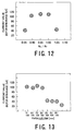
- FIG. 12 is a graph showing a relationship between the shape of the voltage non-linear resistor 2 and the discharge withstand current rating.
- a diameter of the central portion of the voltage non-linear resistor 2 in a thickness direction was set as R6, and a diameter of the end portion thereof was set as R7, and then, the ratio of R7/R7 was measured.
- the voltage non-linear resistor unit 1 was manufactured by using the jig such as the supporting base 7 and the supporting rod 8, and then, the discharge withstand current rating test was carried out with respect to the voltage non-linear resistor unit 1 thus manufactured.
- the jig such as the supporting base 7 and the supporting rod 8
- the abscissa takes a ratio R6/R7, and the ordinate takes a current value before breakage when energizing an impulse current, which is plotted.
- the ratio R6/R7 exceeds a range of 0.9 ⁇ R6/R7 ⁇ 1, the discharge withstand current rating characteristic was greatly reduced.
- FIG. 13 is a graph showing a relationship between the parallelism of the voltage non-linear resistor 2 and the discharge withstand current rating. As is evident from FIG. 13, if the parallelism exceeds a value of 20/100, the discharge withstand current rating characteristic was greatly reduced.
- soldering material 3 an Sn-Pb based eutectic solder is used as the soldering material. It is preferable in term of prevention of environmental pollution to use a solder having a little content of Pb as the soldering material 3. Therefore, by using the soldering material 3 having a content of Pb by 0.1wt% or less and a melting point of 210°C or more, it is possible to provide the voltage non-linear resistor unit 1 which is excellent in the prevention of the environmental pollution.
- soldering material in which Sn is used as a main component, and at least one of Cu, Ag and Sb is contained, and further, the soldering material consists of a low melting point metallic portion having a range such that Sn is 70 to 99%, Ag is 3 to 20% and Cu and Sb are 5% or less.
- the soldering material 3 is specially excellent in Young's modulus and a tensile strength, and the voltage non-linear resistor unit 1 using the soldering material has a stable bonding strength under a high temperature environment.
- each of the soldering materials 3 shown in the Table 1 was formed into a disc-shaped foil, and then, was interposed between the voltage non-linear resistor 2 shown in FIG. 6 and the terminal metal fitting 4. Thereafter, a flux was applied thereto, and a jig such as the supporting base 7 and the supporting rod 8 shown in FIG. 3 and FIG. 4 was used. Then, the voltage non-linear resistor unit 1 was heated under a predetermined condition, and thus, was manufactured. More specifically, the jig was attached to a tap provided in the terminal metal fitting 4, and then, the tensile strength was measured in a state that the voltage non-linear resistor unit 1 thus manufactured was inserted into a thermostatic oven at 120°C. The above test result was shown in the Table 1.
- the voltage non-linear resistor unit 1 consisting of Pb of 0.1% or less, Ag of 3 to 20% or Cu and Sb of 5%, and the remainder of Sn, has a bonding strength of 0.85MPa under a high temperature and is excellent in a strength characteristic. Therefore, it is possible to provide a voltage non-linear resistor unit 1 which is excellent in a stability.
- the voltage non-linear resistor 2 has been joined by applying a flux to the electrode film forming surface with the use of a low melting point metal foil as the soldering material 3. It is also possible to use a paste-like soldering material which is made by integrating a low melting point metal with a flux. It is preferable that the paste-like soldering material consists of a flux portion using a spherical low melting point metal portion having a diameter of 60 ⁇ m or less and zinc chloride as a main component. In the case of using the paste-like soldering material, a working efficiency can be improved.
- FIG. 14 is a graph showing a relationship between a diameter and a bonding strength of a low melting point metal contained in the paste-like soldering material. As is evident from FIG. 14, in the case where a diameter of the low melting point metal portion is 60 ⁇ m or more, a flux is previously volatile, and a wettability becomes worse, resulting in a reduced bonding strength.
- FIG. 15 is a graph showing a relationship between a thickness and a bonding strength of a low melting point metal contained in the paste-like soldering material.
- FIG. 15 there is shown a relationship between the thickness of the low melting point metal and the discharge withstand current rating characteristic when the paste-like solder was applied to the voltage non-linear resistor 2, and then, the voltage non-linear resistors 2 were joined under a predetermined condition.
- the thickness of the low melting point metal exceeds a value of 300 ⁇ m, the discharge withstand current rating characteristic was greatly reduced.
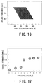
- FIG. 16 is a graph showing a relationship between an applying condition of the paste-like soldering material and a discharge withstand current rating.
- a slanted portion shows a region where the discharge withstand current rating characteristic is 100kA or more.
- the paste-like soldering material occupies an area of 60 to 90% of the joint surface of the voltage non-linear resistors 2 and is formed so as to provide an applied thickness of 0.2 to 1mm.
- the following applying condition is set such that in a range from 60 to 70% of an area of the joined surface, an applied thickness is situated above a straight line connecting the terminations, and in a range from 80 to 90% thereof, the applied thickness is situated below the straight line connecting the terminations, and thereby, it is possible to control a thickness of the low melting point metal, after joined to 300 ⁇ m.
- FIG. 17 is a graph showing a relationship between a compression load and a bonding strength when manufacturing a voltage non-linear resistor unit 1.
- the abscissa takes a pressing force in joining
- the ordinate takes a bonding strength.
- the voltage non-linear resistor unit 1 has a high bonding strength of 1.0MPa. Therefore, it is possible to provide an excellent ZnO device unit. This is because the voltage non-linear resistor unit 1 is heated while a load in joining being applied thereto so as to reduce a pore of the solder.
- the shape of the soldering material after being joined gives an influence to the bonding strength. That is, the soldering material 3 is entirely spread to the joint outer peripheral surface between the voltage non-linear resistor 2 and the terminal metal fitting 4, and then, must be continuously and smoothly formed so as to provide a circular arc-shape from the side of the terminal metal fitting 4 to the joint surface of the voltage non-linear resistor 2. In order to form the shape as described above, when joining the soldering material 3, the heat source is abutted against a local portion of the joint portion while rotating voltage non-linear resistor 2.
- the heat By giving a heat collectively to the local portion of the joint portion by the heat source, the heat is not ridded by the voltage non-linear resistor 2, and therefore, the soldering material 3 can be effectively melted. At the time of being rotated, the heat can be transferred to the joint portion, and it is possible to continuously and smoothly form the soldering material in shape of a circular arc. In this case, since the joint is carried out while applying a load, the effect can be further obtained.
- a generated heat is locally controlled by employing an induction heating method by arranging a coil around the terminal metal fitting 4 as the heat source 9, and using a high frequency current, a beam collection heating method of using a heat source such as a halogen lamp or the like, a burner heat method of using a burner, and a heat fan using an electric heating wire.
- FIG. 18 shows a relationship between the temperature rising speed and the bonding strength. As is evident from FIG. 18, in the case where the temperature rising speed is 10 °C /min or less, the bonding strength is greatly reduced.
- the bonding strength was investigated with respect to a voltage non-linear resistor unit 1 formed by using these materials and a voltage non-linear resistor unit 1 formed by using an aluminum material as a comparative example. In the above test, a jig was attached to a tap provided in the terminal metal fitting 4, and then, a tensile strength was measured. The test result is as shown in the following Table 2. In the Table 2, a mark * shows a comparative example. Material quality of terminal metal fitting Strength(MPa) 1* aluminum alloy(AA2011) 0.45 2 steel material 1.10 3 copper(JIS C1020) 1.05 4 copper alloy(JIS C5212) 1.12 5 brass(JIS C2680) 1.15
- the bonding strength is 1.0MPa or more, and therefore, it is possible to provide a ZnO device unit which is excellent in the bonding strength. Moreover, it was confirmed that the same effects as those mentioned before can be obtained by the materials other than the those in the examples 2 to 5 shown in the Table 2, that is, steel, copper and a copper alloy.
- the bonding strength was greatly reduced.
- the terminal metal fitting 4 was subjected to a plating treatment, and thereby, it is possible to improve the bonding strength. That is, the terminal metal fitting 4 made of aluminum or an aluminum alloy was subjected to Ni, Sn or Zn plating, and thereafter, a voltage non-linear resistor unit 1 was manufactured.
- the bonding strength test was carried out with respect to the voltage non-linear resistor unit 1 thus manufactured in the same manner as in the above-described examples 2 to 5. The test result is shown in the following Table 3.
- Base material Aluminum (AA1050) No. Plating material Strength(MPa) 1 Ni 1.05 2 Sn 1.12 3 Zn 1.05
- the bonding strength is 1.0MPa or more, and therefore, it is possible to provide a ZnO device unit which is excellent in a bonding strength. Moreover, it was confirmed that the same effect can be obtained in the materials other than the examples 1 to 3 shown in the Table 3, that is, aluminum, an aluminum alloy steel, copper or a copper alloy.
- the terminal metal fitting 4 has a structure, in accordance with the shape of the voltage non-linear resistor 2, that the joint surface is formed like a disc, and then, the central portion on the side opposite to the joint surface is formed with a projected screw portion having a diameter of 1/3 of or more than the terminal metal fitting 4 of the jointed portion, and thus, the terminal metal fitting 4 is applied to the voltage non-linear resistor unit 1. Accordingly, it is possible to manufacture an arrester unit having a second terminal metal fitting described later fixed the terminal metal fitting 4 by a screw. In this case, the diameter of the projected screw portion has been set to 1/3 or more of the terminal metal fitting of the joint portion. The reason is because of preventing a deformation in the case where a load is applied in a transverse direction.
- the abscissa takes the minimum thickness of the terminal metal fitting, and the ordinate takes a bonding strength.
- the minimum thickness of the joint portion of the terminal metal fitting 4 is set to 2mm or more, and the bonding strength becomes 1.0MPa or more. Therefore, it is possible to provide a ZnO device unit which is excellent in the bonding strength.
- the bonding strength becomes 1.0MPa or more. Therefore, it is possible to provide a voltage non-linear resistor unit which is excellent in the stable bonding strength, whereby it becomes possible to securely join the voltage non-linear resistor 2 and to provide a voltage non-linear resistor unit 1 which can contribute to a compact size of transformer equipment.
- FIG. 20 is a cross sectional view showing an arrester unit 16 according to one embodiment of the present invention.
- the arrester unit 16 is applicable to a column arrester, a distribution arrester, an arrester for transmission line and the like.
- the arrester unit 16 is composed of a voltage non-linear resistor unit 1, a perforated insulative tube 17 covering the voltage non-linear resistor unit 1, a metallic disc 18 having a through hole, a second terminal metal fitting 19 attached to the terminal metal fitting 4 of the voltage non-linear resistor unit 1, and an elastic insulating cover member 20 covering the components other than the second terminal metal fitting 19.
- the voltage non-linear resistor unit 1 manufactured in any one of the above-described embodiments is used.
- the voltage non-linear resistor unit 1 is covered with a thermosetting perforated insulating tube 17, and then, the metallic disc 18 is inserted into the projected screw portion of the terminal metal fitting 4 on both the end sides of the voltage non-linear resistor unit 1, and thereafter, the second terminal fitting 19 is fixed by means of screw so that the perforated insulating tube is held therebetween.
- the unit thus assembled is put in a baking furnace, and then, is thermally hardened at a temperature of 200°C or less.
- the unit is set in a mold having a predetermined shape and is covered by the elastic insulating covering member 20. Then, the unit is thermally hardened at a temperature of 200 °C or less, and thus, the arrester unit 16 can be obtained.
- the metallic disc 18 includes a plurality of convex protrusions at a side facing the voltage non-linear resistor unit 1, and the perforated insulating tube 17 can be firmly held.
- the second terminal metal fitting 19 including a screw portion 21 at its both sides is used. More specifically, the second terminal metal fitting 19 can be engaged with the terminal metal fitting 4 of the voltage non-linear resistor unit 1 by means of screw and includes the screw portion 21 which is cylindrically extended and has a concave portion at the center of the upper portion so as to directly combine the arrester unit 16 in series.
- the second terminal metal fitting 19 since the side portion of the second terminal metal fitting 19 is set to an arithmetic average surface roughness (central line average surface roughness) of 100 ⁇ m or more, the second terminal metal fitting 19 is preferably engaged with the elastic insulating cover member 20. Therefore, the elastic insulating cover member 20 is not peeled off even if it receives an external force, an ambient temperature and an internal heating effect. As a result, it is possible to prevent an insulative function from being reduced by sucking a moisture due to the peeling.
- the voltage non-linear resistor unit 1 is covered with the thermosetting perforated insulating tube 17. This serves to prevent each component of the arrester from being scattered in the case where the arrester is broken by an excessive surge coming therethrough. Moreover, when an internal pressure rises up by an excessive surge coming therethrough, the internal pressure is uniformly dispersed, and it is possible to prevent a stress from being concentrated in breakage.
- the elastic insulating cover member 20 is formed with a thin wall portion 22 at one side. As shown in FIG. 22, the elastic insulating cover member 20 is formed with a slit-like thin wall portion 22 in a vertical direction, and as shown in FIG. 23, the elastic insulating cover member 20 is formed with a circular-shaped thin wall portion in a vertical direction. The thin wall portion 22 is formed so as to control an arc discharge to one direction.
Landscapes
- Engineering & Computer Science (AREA)
- Microelectronics & Electronic Packaging (AREA)
- Physics & Mathematics (AREA)
- Electromagnetism (AREA)
- Thermistors And Varistors (AREA)
- Details Of Resistors (AREA)
Applications Claiming Priority (2)
| Application Number | Priority Date | Filing Date | Title |
|---|---|---|---|
| JP11201672A JP2001028303A (ja) | 1999-07-15 | 1999-07-15 | 電圧非直線抵抗体ユニットおよび避雷器ユニット |
| JP20167299 | 1999-07-15 |
Publications (2)
| Publication Number | Publication Date |
|---|---|
| EP1069574A2 true EP1069574A2 (fr) | 2001-01-17 |
| EP1069574A3 EP1069574A3 (fr) | 2002-08-28 |
Family
ID=16444996
Family Applications (1)
| Application Number | Title | Priority Date | Filing Date |
|---|---|---|---|
| EP00115336A Withdrawn EP1069574A3 (fr) | 1999-07-15 | 2000-07-14 | Résistance non linéaire en fonction de la tension et limiteur de surtension |
Country Status (6)
| Country | Link |
|---|---|
| US (1) | US6344789B1 (fr) |
| EP (1) | EP1069574A3 (fr) |
| JP (1) | JP2001028303A (fr) |
| CN (1) | CN1152391C (fr) |
| CA (1) | CA2313914C (fr) |
| TW (1) | TW468185B (fr) |
Cited By (2)
| Publication number | Priority date | Publication date | Assignee | Title |
|---|---|---|---|---|
| FR2799301A1 (fr) * | 1999-10-04 | 2001-04-06 | Toshiba Kk | Corps de resistance electrique non lineaire et son procede de fabrication |
| DE102015214938A1 (de) * | 2015-08-05 | 2017-02-09 | Siemens Aktiengesellschaft | Überspannungsableiter mit mehreren Säulen von Widerständen, bei dem die Säulen an einem Ende mit einer Haltevorrichtung befestigt sind, sowie ein Verfahren zur Montage eines Überspannungsableiters |
Families Citing this family (9)
| Publication number | Priority date | Publication date | Assignee | Title |
|---|---|---|---|---|
| JP2008078286A (ja) * | 2006-09-20 | 2008-04-03 | Toshiba Corp | サージアブソーバ |
| EP2144256B1 (fr) | 2008-07-09 | 2011-03-16 | Kabushiki Kaisha Toshiba | Résistance non linéaire de courant/tension |
| JP5301320B2 (ja) * | 2009-03-02 | 2013-09-25 | 三菱電機株式会社 | 避雷器 |
| MX2011011951A (es) | 2009-05-13 | 2012-01-20 | Schlumberger Technology Bv | Sistema y metodo para hacer operaciones de contencion en el sitio de un pozo. |
| MX2011008109A (es) * | 2011-08-01 | 2012-02-23 | Mappec Materiales Productos Polimericos Y Elementos De Construccion S A De C V | Dispositivo protector de sobretensión con mecanismo para liberar presión. |
| JP2013229362A (ja) * | 2012-04-24 | 2013-11-07 | Toshiba Corp | ポリマー避雷器 |
| CN203733541U (zh) * | 2013-12-24 | 2014-07-23 | 爱普科斯公司 | 变阻器器件 |
| KR102282785B1 (ko) * | 2017-11-28 | 2021-07-29 | 엔지케이 인슐레이터 엘티디 | 도전성 선단 부재 및 그 제조 방법 |
| US11037709B2 (en) * | 2018-03-26 | 2021-06-15 | Panasonic Intellectual Property Management Co., Ltd. | Varistor and manufacturing method thereof |
Citations (3)
| Publication number | Priority date | Publication date | Assignee | Title |
|---|---|---|---|---|
| EP0335480A2 (fr) * | 1988-03-31 | 1989-10-04 | Hubbell Incorporated | Ensembles modulaires électriques à décharge de pression |
| WO1999018642A1 (fr) * | 1997-10-08 | 1999-04-15 | Joslyn Manufacturing Co. | Limiteur de surtension a un seul bloc de limitation de surtension |
| JP2000021609A (ja) * | 1998-06-29 | 2000-01-21 | Toshiba Corp | 避雷器 |
Family Cites Families (9)
| Publication number | Priority date | Publication date | Assignee | Title |
|---|---|---|---|---|
| JPS5586680A (en) * | 1978-12-25 | 1980-06-30 | Matsushita Electric Ind Co Ltd | Soldering method of voltage nonlinear resistor |
| US4298900A (en) * | 1980-01-02 | 1981-11-03 | Avdeenko Boris K | Overvoltage protective device |
| US4444351A (en) * | 1981-11-16 | 1984-04-24 | Electric Power Research Institute, Inc. | Method of soldering metal oxide varistors |
| US4423404A (en) * | 1982-02-01 | 1983-12-27 | Electric Power Research Institute, Inc. | Non-linear resistor stack and its method of assembly |
| US5959822A (en) * | 1995-12-22 | 1999-09-28 | Hubbell Incorporated | Compact lightning arrester assembly |
| JP3543046B2 (ja) | 1996-08-07 | 2004-07-14 | 日本碍子株式会社 | 避雷素子ユニットおよびその製造方法 |
| JP3254399B2 (ja) * | 1997-02-03 | 2002-02-04 | ティーディーケイ株式会社 | 積層チップバリスタ及びその製造方法 |
| JPH10270214A (ja) * | 1997-03-28 | 1998-10-09 | Toshiba Corp | 非直線抵抗体の積層接合体 |
| JPH10275737A (ja) * | 1997-03-28 | 1998-10-13 | Toshiba Corp | セラミック素子とその製造方法 |
-
1999
- 1999-07-15 JP JP11201672A patent/JP2001028303A/ja active Pending
-
2000
- 2000-07-14 US US09/617,115 patent/US6344789B1/en not_active Expired - Fee Related
- 2000-07-14 CA CA002313914A patent/CA2313914C/fr not_active Expired - Fee Related
- 2000-07-14 EP EP00115336A patent/EP1069574A3/fr not_active Withdrawn
- 2000-07-14 CN CNB001207792A patent/CN1152391C/zh not_active Expired - Fee Related
- 2000-07-15 TW TW089114192A patent/TW468185B/zh not_active IP Right Cessation
Patent Citations (3)
| Publication number | Priority date | Publication date | Assignee | Title |
|---|---|---|---|---|
| EP0335480A2 (fr) * | 1988-03-31 | 1989-10-04 | Hubbell Incorporated | Ensembles modulaires électriques à décharge de pression |
| WO1999018642A1 (fr) * | 1997-10-08 | 1999-04-15 | Joslyn Manufacturing Co. | Limiteur de surtension a un seul bloc de limitation de surtension |
| JP2000021609A (ja) * | 1998-06-29 | 2000-01-21 | Toshiba Corp | 避雷器 |
Non-Patent Citations (1)
| Title |
|---|
| PATENT ABSTRACTS OF JAPAN vol. 2000, no. 04 31 August 2000 (2000-08-31) * |
Cited By (2)
| Publication number | Priority date | Publication date | Assignee | Title |
|---|---|---|---|---|
| FR2799301A1 (fr) * | 1999-10-04 | 2001-04-06 | Toshiba Kk | Corps de resistance electrique non lineaire et son procede de fabrication |
| DE102015214938A1 (de) * | 2015-08-05 | 2017-02-09 | Siemens Aktiengesellschaft | Überspannungsableiter mit mehreren Säulen von Widerständen, bei dem die Säulen an einem Ende mit einer Haltevorrichtung befestigt sind, sowie ein Verfahren zur Montage eines Überspannungsableiters |
Also Published As
| Publication number | Publication date |
|---|---|
| CN1152391C (zh) | 2004-06-02 |
| CA2313914C (fr) | 2004-05-04 |
| US6344789B1 (en) | 2002-02-05 |
| JP2001028303A (ja) | 2001-01-30 |
| TW468185B (en) | 2001-12-11 |
| CA2313914A1 (fr) | 2001-01-15 |
| EP1069574A3 (fr) | 2002-08-28 |
| CN1281230A (zh) | 2001-01-24 |
Similar Documents
| Publication | Publication Date | Title |
|---|---|---|
| US5907274A (en) | Chip resistor | |
| US6043973A (en) | Ceramic capacitor | |
| US4296002A (en) | Metal oxide varistor manufacture | |
| US6344789B1 (en) | Voltage non-linear resistor unit and arrester unit | |
| US4053864A (en) | Thermistor with leads and method of making | |
| EP3109868B1 (fr) | Procédé de préparation de composants électroniques avec une couche d'électrode en alliage | |
| KR101022980B1 (ko) | 세라믹 전자 부품 | |
| US4538347A (en) | Method for making a varistor package | |
| US6840432B1 (en) | Solder application technique | |
| EP0797220B1 (fr) | Composition résistive et résistances utilisant celle-ci | |
| US6898071B2 (en) | Electrical multilayer component and method for the production thereof | |
| JP2023071558A (ja) | 積層バリスタ及びその製造方法 | |
| US12094642B2 (en) | Multilayer inductor component | |
| US6163245A (en) | Nonlinear resistor with electrodes formed by plasma spraying | |
| CN111052270A (zh) | 厚膜电阻膏以及厚膜电阻膏在电阻器中的用途 | |
| JP2004152824A (ja) | チップ状電子部品およびその製造方法 | |
| JP3915188B2 (ja) | チップ抵抗器及びその製造方法 | |
| CN121970129A (zh) | 层叠型电阻器及层叠型电阻器的制造方法 | |
| JPH09275002A (ja) | 厚膜抵抗体とそれを用いたチップ抵抗器およびその製造方法 | |
| JPH10275737A (ja) | セラミック素子とその製造方法 | |
| JP2002217005A (ja) | 非直線抵抗体およびその製造方法 | |
| JP2003109806A (ja) | 非直線抵抗体及びその製造方法 | |
| US20230274863A1 (en) | Multilayer varistor | |
| JPH10270214A (ja) | 非直線抵抗体の積層接合体 | |
| JP2000277302A (ja) | セラミック素子ユニット及びその製造方法 |
Legal Events
| Date | Code | Title | Description |
|---|---|---|---|
| PUAI | Public reference made under article 153(3) epc to a published international application that has entered the european phase |
Free format text: ORIGINAL CODE: 0009012 |
|
| 17P | Request for examination filed |
Effective date: 20000714 |
|
| AK | Designated contracting states |
Kind code of ref document: A2 Designated state(s): AT BE CH CY DE DK ES FI FR GB GR IE IT LI LU MC NL PT SE |
|
| AX | Request for extension of the european patent |
Free format text: AL;LT;LV;MK;RO;SI |
|
| PUAL | Search report despatched |
Free format text: ORIGINAL CODE: 0009013 |
|
| AK | Designated contracting states |
Kind code of ref document: A3 Designated state(s): AT BE CH CY DE DK ES FI FR GB GR IE IT LI LU MC NL PT SE |
|
| AX | Request for extension of the european patent |
Free format text: AL;LT;LV;MK;RO;SI |
|
| RIC1 | Information provided on ipc code assigned before grant |
Free format text: 7H 01C 7/12 A, 7H 01C 7/112 B |
|
| AKX | Designation fees paid |
Designated state(s): DE FR SE |
|
| STAA | Information on the status of an ep patent application or granted ep patent |
Free format text: STATUS: THE APPLICATION IS DEEMED TO BE WITHDRAWN |
|
| 18D | Application deemed to be withdrawn |
Effective date: 20060802 |