EP1065733A2 - Licht-emittierende Diode und Herstellungsverfahren - Google Patents
Licht-emittierende Diode und Herstellungsverfahren Download PDFInfo
- Publication number
- EP1065733A2 EP1065733A2 EP00113711A EP00113711A EP1065733A2 EP 1065733 A2 EP1065733 A2 EP 1065733A2 EP 00113711 A EP00113711 A EP 00113711A EP 00113711 A EP00113711 A EP 00113711A EP 1065733 A2 EP1065733 A2 EP 1065733A2
- Authority
- EP
- European Patent Office
- Prior art keywords
- light emitting
- electrode
- emitting diode
- emitting structure
- region
- Prior art date
- Legal status (The legal status is an assumption and is not a legal conclusion. Google has not performed a legal analysis and makes no representation as to the accuracy of the status listed.)
- Withdrawn
Links
- 238000004519 manufacturing process Methods 0.000 title claims description 12
- 238000003776 cleavage reaction Methods 0.000 claims abstract description 49
- 230000007017 scission Effects 0.000 claims abstract description 49
- SBIBMFFZSBJNJF-UHFFFAOYSA-N selenium;zinc Chemical compound [Se]=[Zn] SBIBMFFZSBJNJF-UHFFFAOYSA-N 0.000 claims abstract description 43
- 230000007547 defect Effects 0.000 claims abstract description 25
- 239000004065 semiconductor Substances 0.000 claims description 39
- 239000000463 material Substances 0.000 claims description 27
- 239000000758 substrate Substances 0.000 claims description 22
- 230000001629 suppression Effects 0.000 claims description 21
- 239000013078 crystal Substances 0.000 claims description 13
- 238000005530 etching Methods 0.000 claims description 10
- VYPSYNLAJGMNEJ-UHFFFAOYSA-N Silicium dioxide Chemical compound O=[Si]=O VYPSYNLAJGMNEJ-UHFFFAOYSA-N 0.000 claims description 6
- PNEYBMLMFCGWSK-UHFFFAOYSA-N aluminium oxide Inorganic materials [O-2].[O-2].[O-2].[Al+3].[Al+3] PNEYBMLMFCGWSK-UHFFFAOYSA-N 0.000 claims description 3
- 229910052681 coesite Inorganic materials 0.000 claims description 3
- 150000001875 compounds Chemical class 0.000 claims description 3
- 229910052593 corundum Inorganic materials 0.000 claims description 3
- 229910052906 cristobalite Inorganic materials 0.000 claims description 3
- 238000005520 cutting process Methods 0.000 claims description 3
- 229910052737 gold Inorganic materials 0.000 claims description 3
- AMGQUBHHOARCQH-UHFFFAOYSA-N indium;oxotin Chemical compound [In].[Sn]=O AMGQUBHHOARCQH-UHFFFAOYSA-N 0.000 claims description 3
- 229910052759 nickel Inorganic materials 0.000 claims description 3
- 229910052763 palladium Inorganic materials 0.000 claims description 3
- 238000001020 plasma etching Methods 0.000 claims description 3
- 239000000377 silicon dioxide Substances 0.000 claims description 3
- 238000000992 sputter etching Methods 0.000 claims description 3
- 229910052682 stishovite Inorganic materials 0.000 claims description 3
- 229910052905 tridymite Inorganic materials 0.000 claims description 3
- 229910001845 yogo sapphire Inorganic materials 0.000 claims description 3
- 230000002093 peripheral effect Effects 0.000 claims description 2
- 229910007709 ZnTe Inorganic materials 0.000 description 11
- 230000008020 evaporation Effects 0.000 description 8
- 238000001704 evaporation Methods 0.000 description 8
- 238000005253 cladding Methods 0.000 description 4
- 230000015572 biosynthetic process Effects 0.000 description 3
- 239000000956 alloy Substances 0.000 description 2
- 229910045601 alloy Inorganic materials 0.000 description 2
- 238000000151 deposition Methods 0.000 description 2
- 238000002347 injection Methods 0.000 description 2
- 239000007924 injection Substances 0.000 description 2
- 238000000034 method Methods 0.000 description 2
- 230000004888 barrier function Effects 0.000 description 1
- 230000003247 decreasing effect Effects 0.000 description 1
- 230000008021 deposition Effects 0.000 description 1
- 230000000694 effects Effects 0.000 description 1
- 238000000059 patterning Methods 0.000 description 1
- 238000000926 separation method Methods 0.000 description 1
- 238000001039 wet etching Methods 0.000 description 1
Images


Classifications
-
- H—ELECTRICITY
- H10—SEMICONDUCTOR DEVICES; ELECTRIC SOLID-STATE DEVICES NOT OTHERWISE PROVIDED FOR
- H10H—INORGANIC LIGHT-EMITTING SEMICONDUCTOR DEVICES HAVING POTENTIAL BARRIERS
- H10H20/00—Individual inorganic light-emitting semiconductor devices having potential barriers, e.g. light-emitting diodes [LED]
- H10H20/80—Constructional details
- H10H20/83—Electrodes
- H10H20/832—Electrodes characterised by their material
-
- H—ELECTRICITY
- H10—SEMICONDUCTOR DEVICES; ELECTRIC SOLID-STATE DEVICES NOT OTHERWISE PROVIDED FOR
- H10H—INORGANIC LIGHT-EMITTING SEMICONDUCTOR DEVICES HAVING POTENTIAL BARRIERS
- H10H20/00—Individual inorganic light-emitting semiconductor devices having potential barriers, e.g. light-emitting diodes [LED]
- H10H20/80—Constructional details
- H10H20/81—Bodies
- H10H20/822—Materials of the light-emitting regions
- H10H20/823—Materials of the light-emitting regions comprising only Group II-VI materials, e.g. ZnO
-
- H—ELECTRICITY
- H10—SEMICONDUCTOR DEVICES; ELECTRIC SOLID-STATE DEVICES NOT OTHERWISE PROVIDED FOR
- H10H—INORGANIC LIGHT-EMITTING SEMICONDUCTOR DEVICES HAVING POTENTIAL BARRIERS
- H10H20/00—Individual inorganic light-emitting semiconductor devices having potential barriers, e.g. light-emitting diodes [LED]
- H10H20/80—Constructional details
- H10H20/83—Electrodes
- H10H20/832—Electrodes characterised by their material
- H10H20/833—Transparent materials
Definitions
- the present invention relates to light emitting diodes and manufacturing methods thereof. More specifically, the present invention relates to a homoepitaxial ZnSe-based light emitting diode (hereinafter, referred to as an LED) which has a ZnSe single crystal substrate and a light emitting structure including a mixed crystal compound semiconductor made of ZnSe or mainly of ZnSe, as well as a manufacturing method thereof.
- an LED homoepitaxial ZnSe-based light emitting diode
- the LED has a light emitting structure formed on a ZnSe substrate and an electrode formed thereon.
- the LED is formed by depositing various semiconductor layers on the ZnSe substrate such as by epitaxial growth, forming an electrode thereon, cutting them into a chip of a prescribed size, and then fixing it to a lead frame.
- the defects near the cleavage plane can be addressed by etching and removing a portion near the cleavage plane. In this case, however, it is necessary to cope with a side etching phenomenon which is caused by a difference in the etching rates of the semiconductor layers.
- An object of the present invention is to provide a higher luminance value and a longer life for an LED without using complex processes.
- a light emitting diode includes a ZnSe substrate and a light emitting structure formed on the substrate. It is noted herein that the light emitting structure refers to a stacked structure of semiconductor layers including a light emitting layer.
- the light emitting diode having the above described structure includes a current restriction region for suppressing the increase in the density of defects by restricting the path of the injected current for light emission.
- the injected current restriction region By thus providing the injected current restriction region, it is possible to restrict or prevent a current flow into the region and to suppress the increase in the defect density in the region. Especially by selecting a region having a large number of defects as the injected current restriction region, it is possible to realize a longer life and a higher luminance value for the LED.
- the above described light emitting diode is a homoepitaxial ZnSe-based light emitting diode.
- the ZnSe substrate is a conductive ZnSe single crystal substrate, and the light emitting structure includes a mixed crystal compound semiconductor made of ZnSe or mainly of ZnSe.
- the present invention is particularly effective for the homoepitaxial ZnSe-based light emitting diode as described above.
- the light emitting diode includes a cleavage plane for cutting an element to be separated.
- the injected current restriction region preferably includes a region near the cleavage plane.
- a large number of defects may exist near the cleavage plane of a light emitting diode. Therefore, by suppressing a current flow into such a region having a large number of defects, it is possible to realize a longer life and a higher luminance value for the LED.
- the light emitting diode has an ohmic electrode on the light emitting structure.
- the ohmic electrode is positioned to be apart from the above described cleavage plane.
- the ohmic electrode By providing the ohmic electrode to be apart from the cleavage plane, it is possible to suppress a current flow into the vicinity of the cleavage plane. It is therefore possible to realize a longer life and a higher luminance value for the LED. Since the position of an end of the electrode only needs to be adjusted, the LED can be given a longer life and a higher luminance value without complex processes.
- the above described ohmic electrode is formed to be isolated from the cleavage plane by at least 5 ⁇ m, and the diode has an electrode for wire bonding.
- the longer life of the LED can be effectively provided by not forming the ohmic electrode for diffusing an injected current at least in the region.
- the above described electrode is a light transmitting electrode and includes at least one material selected from the group consisting of Au, Pd, Ni and ITO (Indium Tin Oxide).
- the light emitting diode according to the present invention may have, on the light emitting structure, a first electrode made of a material not attaining ohmic contact with the light emitting structure for restricting an injected current, and a second electrode made of a material attaining ohmic contact with the light emitting structure for diffusing an injected current. It is preferred in this case that the first electrode is formed on the region near the cleavage plane and the second electrode is formed on a region other than the region near the cleavage plane.
- the first electrode does not attain ohmic contact with the light emitting structure, a current flow from the first electrode into the light emitting structure can be suppressed. In other words, a current flow into a region under the first electrode can be suppressed. It is therefore possible to suppress an increase in defects in the region under the first electrode.
- a current can be applied from the second electrode into the light emitting structure, causing the LED to emit light.
- the light emitting diode may have a semiconductor layer selectively provided inside the light emitting structure and not attaining ohmic contact with the first electrode, and a trench portion provided at an upper surface peripheral portion of the light emitting structure and extending to the cleavage plane and the semiconductor layer.
- the first electrode is formed on the trench portion to be in contact with the semiconductor layer.
- the trench is formed by etching. More specifically, the trench is preferably formed by such etching that emphasizes irregularity on the trench surface, for example, ion milling and reactive ion etching.
- the above described first electrode is formed at least on a region within 5 ⁇ m from the cleavage plane and includes at least one material selected from the group consisting of Ti, Al, ZnS, Al 2 O 3 , SiO 2 and SiN.
- the first electrode By forming the first electrode on the region as described above, it is possible to prevent a current flow into the region within 5 ⁇ m from the cleavage plane.
- a current suppression layer for suppressing a current flow may be provided inside the light emitting structure near the cleavage plane.
- the light emitting diode may include a first electrode for restricting an injected current, provided on such a surface portion of the light emitting structure that is located on the above described current suppression layer and made of a material not attaining ohmic contact with the current suppression layer, and a second electrode for diffusing an injected current, provided on such a surface portion of the light emitting structure that is located on a region where the current suppression layer is not formed and made of a material attaining ohmic contact with the light emitting structure.
- the first electrode using the material not attaining ohmic contact with the current suppression layer, it is possible to suppress a current flow into the region under the current suppression layer even if a certain conductive layer exists between the first electrode and the current suppression layer. It is therefore possible to suppress the increase in the density of defects in the region under the current suppression layer.
- a light emitting diode manufacturing method includes the steps of: forming a light emitting structure on a ZnSe substrate; forming, on a first surface region of the light emitting structure, a first electrode made of a material not attaining ohmic contact with the light emitting structure for restricting an injected current; and forming, on a second surface region of the light emitting structure, a second electrode made of a material attaining ohmic contact with the light emitting structure for diffusing an injected current.
- the first electrode made of the material not attaining ohmic contact with the light emitting structure By thus forming the first electrode made of the material not attaining ohmic contact with the light emitting structure on the first surface region, it is possible to suppress a current flow into a region immediately under the first surface region. It is therefore possible to suppress the increase in the density of defects in the region. Since the second electrode made of the material attaining ohmic contact with the light emitting structure is formed on the second surface region different from the first surface region, a current can be supplied from the second electrode into the light emitting structure, causing the LED to emit light.
- a light emitting diode manufacturing method includes the steps of: forming a light emitting structure on a ZnSe substrate by sequentially stacking a first semiconductor layer including a light emitting layer, selectively a second semiconductor layer on the first semiconductor layer, and a third semiconductor layer from the top of the semiconductor to the top of the second semiconductor layer; forming, on such a surface portion of the light emitting structure that is located on the second semiconductor layer, a first electrode made of a material not attaining ohmic contact with the second semiconductor layer for restricting an injected current; and forming, on such a surface portion of the light emitting structure that is located on a region where the second semiconductor layer is not formed, a second electrode made of a material attaining ohmic contact with the light emitting structure for diffusing an injected current.
- the above described first to third semiconductor layers are a stacked structure of a plurality of semiconductor layers.
- an important feature of the present invention is to selectively provide an injected current restriction region for restricting an injected current for light emission.
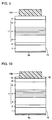
- Fig. 1 is a sectional view of an LED in a first embodiment of the present invention.
- the LED includes a conductive ZnSe single crystal substrate 1, a light emitting structure 12 formed thereon, and a light transmitting Au electrode 9 for diffusing an injected current for light emission, and a base electrode 10.
- the LED is cleaved on a cleavage plane 13 for element separation.
- An In electrode 9a is formed on the back surface of conductive ZnSe single crystal substrate 1.
- Light emitting structure 12 is formed on the top surface of conductive ZnSe single crystal substrate 1.
- Light emitting structure 12 has an n-type ZnSe buffer layer 2 having a thickness of about 1 ⁇ m, an n-type ZnMgSSe cladding layer 3 having a thickness of about 1 ⁇ m, a ZnSe/ZnCdSe multiple quantum well active layer 4, a p-type ZnMgSSe cladding layer 5 having a thickness of about 1 ⁇ m, a p-type ZnSe layer 6 having a thickness of about 0.2 ⁇ m, a p-type contact layer 7 formed of a stacked superlattice structure of ZnSe and ZnTe, and a p-type ZnTe layer 8 having a thickness of about 60nm on the top.
- light emitting structure 12 is formed of the stacked structure of a plurality of semiconductor layers (epitaxial layers) and includes a light emitting layer 11.
- Light emitting layer 11 has n-type ZnMgSSe cladding layer 3, ZnSe/ZnCdSe multiple quantum well active layer 4, and p-type ZnMgSSe cladding layer 5.
- Light transmitting Au electrode 9 and base electrode 10 are formed on the top surface of light emitting structure.
- Base electrode 10 has a Ti layer 10a and an Au layer 10b.
- Light transmitting Au electrode 9 has a thickness of 20nm or less and is formed to be separated from cleavage plane 13 by width D1 (preferably, 5 ⁇ m or more). Thus, light transmitting Au electrode 9 is not formed on a region near cleavage plane 13. It is therefore possible to suppress a current flow into the region near cleavage plane 13 and to suppress an increase in defects in the region.
- the region near cleavage plane 13 is selected as the injected current restriction region in the first embodiment. Since a larger number of defects would exist in the region near cleavage plane 13 than in other regions as described above, it is considered that suppression of a current flow into the region can effectively contribute to a longer life and a higher luminance value of the LED.
- the doping concentration of p-type ZnTe layer 8 is set at 1 ⁇ 10 19 cm -3 or less so as to attain Schottky contact between Ti layer 10a of the base electrode and p-type ZnTe layer 8.
- In electrode 9 is formed such as by evaporation (deposition).
- light emitting structure 12 is formed such as by epitaxial growth.
- Ti layer 10a and Au layer 10b are sequentially stacked such as by evaporation. After they are patterned to a prescribed shape, an Au layer is formed to a thickness of about 20nm or less such as by evaporation again. By patterning the Au layer, a portion near cleavage plane 13 is selectively removed.
- wafer-like ZnSe single crystal substrate 1 and light emitting structure 12 are cut into a chip having a size of 300 ⁇ m for its sides. Thus, cleavage plane 13 is formed. Thereafter, conductive ZnSe single crystal substrate 1 and light emitting structure 12 are fixed to a lead frame.
- the LED in this embodiment is formed through the above described steps.
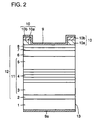
- Fig. 2 is a sectional view of an LED in the second embodiment of the present invention.
- base electrode 10 is placed on a region near cleavage plane 13 in the second embodiment. More specifically, base electrodes 10 are placed in a lattice manner on regions within about 50 ⁇ m from cleavage planes 13 (portions to be cleaved). Light transmitting Au electrode 9 is formed to extend from a region surrounded by base electrodes 10 to the tops of the base electrodes. Since other components are similar to the first embodiment, description thereof will not be repeated.
- the doping concentration of p-type ZnTe layer 8 is also set at 1 ⁇ 10 19 cm -3 or less similarly to the first embodiment. Therefore, a Schottky barrier is formed between Ti layer 10a in base electrode 10 and p-type ZnTe layer 8, which prevents ohmic contact. It is therefore possible to suppress a current flow from base electrode 10 into light emitting structure 12. As a result, similarly to the first embodiment, it is possible to suppress a current flow into a region near cleavage plane 13 and to suppress an increase in defects in the region.
- the LED in this embodiment may be provided by performing similar steps to the first embodiment till formation of p-type ZnTe layer 8 and, thereafter, forming base electrode 10 on the region near cleavage plane 13, and forming light transmitting Au electrode 9 such as by evaporation to cover base electrode 10. Then, the LED can be formed through similar steps to the first embodiment.
- Fig. 3 is a sectional view of an LED in the third embodiment of the present invention.
- an annular trench portion 14 extending to p-type ZnSe layer 6 and cleavage plane 13 is formed, and base electrode 10 is formed inside trench portion 14.
- Width D2 from cleavage plane 13 to trench portion 14 is about 50 ⁇ m, for example. Since other components other than that are similar to the second embodiment, description thereof will not be repeated.
- Fig. 15 illustrates the current supply (injection) test results of the LED in this embodiment and a conventional LED.
- the employed conventional example was provided by forming a light transmitting Au electrode 9 on the entire surface and forming a pad for wire bonding on the chip center.
- the current supply conditions were room temperature and a direct current of 20mA.
- the chip size was 500 ⁇ m for its sides.
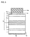
- a trench portion 14 extending to p-type ZnSe layer 6 is formed by etching using resist 16a as a mask as shown in Fig. 5.
- wet etching may be employed although ion milling or reactive ion etching can improve the contact of an electrode and eliminate poor wire bonding.
- Ti layer 10a and Au layer 10b are then deposited sequentially by evaporation. Thereafter, resist 16a is removed to expose the surface of p-type ZnTe layer 8 as shown in Fig. 7. Then, light transmitting electrode 9 is formed on the entire surface such as by evaporation.
- the above described steps result in the structure shown in Fig. 3. Thereafter, similar steps to the first and second embodiments are performed to form the LED.
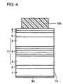
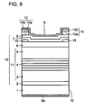
- Fig. 8 is a sectional view of an LED in the fourth embodiment of the present invention.
- a current suppression layer 15 is formed inside light emitting structure in this embodiment. Since other components are similar to the second embodiment, description thereof will not be repeated.
- current suppression layer 15 may be an n-type semiconductor layer or any semiconductor layer which does not attain ohmic contact with Ti layer 10a in base electrode 10.
- Resist 16b is then removed, and p-type contact layer 7 and p-type ZnTe layer 8 are formed to extend from the top of p-type ZnSe layer 6 to the top of current suppression layer 15 by epitaxial growth as shown in Fig. 11.
- a resist 16c is applied on p-type ZnTe layer 8 and patterned to a prescribed shape as shown in Fig. 12.
- Ti layer 10a and Au layer 10b are deposited such as by evaporation to obtain the structure shown in Fig. 13, and then resist 16c is removed.
- the description is based on a case where an injected current restriction region is formed in the region near cleavage plane 13.
- the injected current restriction region may be provided in other regions.
- the light transmitting electrode may be formed of at least one material selected from the group consisting of Au, Pd, Ni and ITO (Indium Tin Oxide) or an alloy containing at least one material of the group.
- the lower layer of base electrode 10 may be formed of at least one material selected from the group consisting of Ti, Al, ZnS, Al 2 O 3 , SiO 2 and SiN or an alloy containing at least one material of the group.
- the injected current restriction region is provided inside the LED and therefore a current for light emission can be prevented from flowing into a desired region in the LED. It is therefore possible to suppress an increase in defects in the region and to realize not only a longer life but also a higher luminance value for the LED. Especially by selecting a region having a large number of defects as the injected current restriction region, a much longer life and a much higher luminance value for the LED can be achieved.
Landscapes
- Led Devices (AREA)
Applications Claiming Priority (2)
| Application Number | Priority Date | Filing Date | Title |
|---|---|---|---|
| JP18760499 | 1999-07-01 | ||
| JP18760499A JP3533995B2 (ja) | 1999-07-01 | 1999-07-01 | 発光ダイオードおよびその製造方法 |
Publications (1)
| Publication Number | Publication Date |
|---|---|
| EP1065733A2 true EP1065733A2 (de) | 2001-01-03 |
Family
ID=16209028
Family Applications (1)
| Application Number | Title | Priority Date | Filing Date |
|---|---|---|---|
| EP00113711A Withdrawn EP1065733A2 (de) | 1999-07-01 | 2000-06-28 | Licht-emittierende Diode und Herstellungsverfahren |
Country Status (6)
| Country | Link |
|---|---|
| US (1) | US6420731B1 (de) |
| EP (1) | EP1065733A2 (de) |
| JP (1) | JP3533995B2 (de) |
| KR (1) | KR20010039677A (de) |
| CN (1) | CN1290967A (de) |
| TW (1) | TW484240B (de) |
Cited By (1)
| Publication number | Priority date | Publication date | Assignee | Title |
|---|---|---|---|---|
| EP1517379A3 (de) * | 2003-09-19 | 2011-07-06 | Sumitomo Electric Industries, Ltd. | Lichtemittierende Halbleitervorrichtung der II-VI-Gruppe |
Families Citing this family (10)
| Publication number | Priority date | Publication date | Assignee | Title |
|---|---|---|---|---|
| JP2002222992A (ja) * | 2001-01-25 | 2002-08-09 | Rohm Co Ltd | Led発光素子、およびled発光装置 |
| KR100404416B1 (ko) * | 2001-07-06 | 2003-11-05 | 주식회사 옵토웨이퍼테크 | 반도체 발광소자 및 그 제조방법 |
| US6730941B2 (en) * | 2002-01-30 | 2004-05-04 | Showa Denko Kabushiki Kaisha | Boron phosphide-based semiconductor light-emitting device, production method thereof, and light-emitting diode |
| KR100674862B1 (ko) * | 2005-08-25 | 2007-01-29 | 삼성전기주식회사 | 질화물 반도체 발광 소자 |
| DE102005061797B4 (de) * | 2005-12-23 | 2020-07-09 | Osram Opto Semiconductors Gmbh | Lumineszenzdiodenchip mit Stromaufweitungsschicht und Verfahren zu dessen Herstellung |
| JPWO2009078482A1 (ja) * | 2007-12-19 | 2011-05-06 | ローム株式会社 | 半導体発光素子 |
| US20120168714A1 (en) * | 2011-01-03 | 2012-07-05 | SemiLEDs Optoelectronics Co., Ltd. | Vertical light emitting diode (vled) die and method of fabrication |
| KR101797598B1 (ko) | 2011-05-26 | 2017-11-15 | 엘지이노텍 주식회사 | 발광소자 |
| KR102066621B1 (ko) * | 2013-08-02 | 2020-01-15 | 엘지이노텍 주식회사 | 발광 소자 |
| CN114078897A (zh) * | 2020-08-19 | 2022-02-22 | 京东方科技集团股份有限公司 | 发光器件及其制备方法、显示面板、背光模组和显示装置 |
Family Cites Families (12)
| Publication number | Priority date | Publication date | Assignee | Title |
|---|---|---|---|---|
| GB2226698B (en) * | 1988-11-15 | 1992-05-20 | Kokusai Denshin Denwa Co Ltd | A light emitting semiconductor device |
| JPH0559861A (ja) | 1991-08-30 | 1993-03-09 | Taamo:Kk | 止 具 |
| JP2859478B2 (ja) | 1991-12-12 | 1999-02-17 | 日亜化学工業 株式会社 | 発光デバイス用の窒化ガリウム系化合物半導体ウエハーの切断方法 |
| JP2765644B2 (ja) | 1992-05-09 | 1998-06-18 | 日亜化学工業株式会社 | 窒化ガリウム系化合物半導体ウエハーの切断方法 |
| US5319219A (en) * | 1992-05-22 | 1994-06-07 | Minnesota Mining And Manufacturing Company | Single quantum well II-VI laser diode without cladding |
| JP3586293B2 (ja) * | 1994-07-11 | 2004-11-10 | ソニー株式会社 | 半導体発光素子 |
| US5838029A (en) * | 1994-08-22 | 1998-11-17 | Rohm Co., Ltd. | GaN-type light emitting device formed on a silicon substrate |
| US5544190A (en) * | 1994-11-17 | 1996-08-06 | Phillips Electronics North America Corporation | II-VI Semiconductor diode laser with lateral current confinement |
| JP3713100B2 (ja) * | 1996-05-23 | 2005-11-02 | ローム株式会社 | 半導体発光素子の製法 |
| JPH10294531A (ja) * | 1997-02-21 | 1998-11-04 | Toshiba Corp | 窒化物化合物半導体発光素子 |
| JPH114020A (ja) * | 1997-04-15 | 1999-01-06 | Toshiba Corp | 半導体発光素子及びその製造方法、並びに半導体発光装置 |
| JP2000124540A (ja) * | 1998-10-16 | 2000-04-28 | Fuji Photo Film Co Ltd | 半導体発光素子 |
-
1999
- 1999-07-01 JP JP18760499A patent/JP3533995B2/ja not_active Expired - Fee Related
-
2000
- 2000-06-22 KR KR1020000034454A patent/KR20010039677A/ko not_active Withdrawn
- 2000-06-23 TW TW089112397A patent/TW484240B/zh not_active IP Right Cessation
- 2000-06-26 US US09/603,855 patent/US6420731B1/en not_active Expired - Fee Related
- 2000-06-28 EP EP00113711A patent/EP1065733A2/de not_active Withdrawn
- 2000-07-03 CN CN00119932A patent/CN1290967A/zh active Pending
Cited By (1)
| Publication number | Priority date | Publication date | Assignee | Title |
|---|---|---|---|---|
| EP1517379A3 (de) * | 2003-09-19 | 2011-07-06 | Sumitomo Electric Industries, Ltd. | Lichtemittierende Halbleitervorrichtung der II-VI-Gruppe |
Also Published As
| Publication number | Publication date |
|---|---|
| CN1290967A (zh) | 2001-04-11 |
| KR20010039677A (ko) | 2001-05-15 |
| JP3533995B2 (ja) | 2004-06-07 |
| JP2001015810A (ja) | 2001-01-19 |
| TW484240B (en) | 2002-04-21 |
| US6420731B1 (en) | 2002-07-16 |
Similar Documents
| Publication | Publication Date | Title |
|---|---|---|
| TWI502769B (zh) | 晶圓級發光二極體結構、發光二極體晶片及其製造方法 | |
| EP1646092B1 (de) | Kontakt und omnidirektionaler Reflektor für Flipchip-Leuchtdioden | |
| EP2296199B1 (de) | Lichtemittierende Halbleitervorrichtung und Herstellungsverfahren davon | |
| US5760423A (en) | Semiconductor light emitting device, electrode of the same device and method of manufacturing the same device | |
| EP2426743B1 (de) | Lichtemittierendes Halbleiterbauelement mit GaN-Verbindung und Verfahren zu dessen Herstellung | |
| US8581295B2 (en) | Semiconductor light-emitting diode | |
| US20020197764A1 (en) | Group III nitride compound semiconductor light-emitting element | |
| EP1202355A2 (de) | Lichtemittierende Vorrichtung und Herstellungsverfahren | |
| JPH114020A (ja) | 半導体発光素子及びその製造方法、並びに半導体発光装置 | |
| JP2007103951A (ja) | 窒化物系半導体発光素子及びその製造方法 | |
| JP5628064B2 (ja) | 光半導体素子 | |
| EP4154324B1 (de) | Subpixel-leuchtdioden für direktansichtsanzeige und verfahren zur herstellung davon | |
| TWI437737B (zh) | 發光二極體結構及其製造方法 | |
| EP1065733A2 (de) | Licht-emittierende Diode und Herstellungsverfahren | |
| TWI466327B (zh) | 晶圓級發光二極體結構之製造方法 | |
| CN1476365A (zh) | 带有用于改善光提取的锥形侧壁的激光分离的管芯 | |
| US6168962B1 (en) | Method of manufacturing a semiconductor light emitting device | |
| JP3934730B2 (ja) | 半導体発光素子 | |
| KR102737506B1 (ko) | 반도체 발광소자 및 그 제조 방법 | |
| KR100631970B1 (ko) | 플립칩용 질화물 반도체 발광소자 | |
| JP2004265923A (ja) | 半導体発光素子およびその製造方法 | |
| US12364081B2 (en) | Light emitting device and method for producing the same | |
| EP1334523A2 (de) | VERBESSERTE LICHTENTNAHMEEFFIZIENZ VON LEDs AUF GaN-BASIS | |
| HK1033031A (en) | Light emitting diode and manufacturing method thereof | |
| JP2001250984A (ja) | Iii族窒化物系化合物半導体素子 |
Legal Events
| Date | Code | Title | Description |
|---|---|---|---|
| PUAI | Public reference made under article 153(3) epc to a published international application that has entered the european phase |
Free format text: ORIGINAL CODE: 0009012 |
|
| AK | Designated contracting states |
Kind code of ref document: A2 Designated state(s): AT BE CH CY DE DK ES FI FR GB GR IE IT LI LU MC NL PT SE |
|
| AX | Request for extension of the european patent |
Free format text: AL;LT;LV;MK;RO;SI |
|
| STAA | Information on the status of an ep patent application or granted ep patent |
Free format text: STATUS: THE APPLICATION HAS BEEN WITHDRAWN |
|
| 18W | Application withdrawn |
Effective date: 20050331 |