EP1052062A1 - Vorbehandlung eines fixierten Schleifmittels - Google Patents
Vorbehandlung eines fixierten Schleifmittels Download PDFInfo
- Publication number
- EP1052062A1 EP1052062A1 EP00303717A EP00303717A EP1052062A1 EP 1052062 A1 EP1052062 A1 EP 1052062A1 EP 00303717 A EP00303717 A EP 00303717A EP 00303717 A EP00303717 A EP 00303717A EP 1052062 A1 EP1052062 A1 EP 1052062A1
- Authority
- EP
- European Patent Office
- Prior art keywords
- projections
- conditioning
- abrasive
- article
- fixed abrasive
- Prior art date
- Legal status (The legal status is an assumption and is not a legal conclusion. Google has not performed a legal analysis and makes no representation as to the accuracy of the status listed.)
- Withdrawn
Links
Images


Classifications
-
- B—PERFORMING OPERATIONS; TRANSPORTING
- B24—GRINDING; POLISHING
- B24B—MACHINES, DEVICES, OR PROCESSES FOR GRINDING OR POLISHING; DRESSING OR CONDITIONING OF ABRADING SURFACES; FEEDING OF GRINDING, POLISHING, OR LAPPING AGENTS
- B24B37/00—Lapping machines or devices; Accessories
- B24B37/11—Lapping tools
- B24B37/20—Lapping pads for working plane surfaces
- B24B37/205—Lapping pads for working plane surfaces provided with a window for inspecting the surface of the work being lapped
-
- H—ELECTRICITY
- H01—ELECTRIC ELEMENTS
- H01L—SEMICONDUCTOR DEVICES NOT COVERED BY CLASS H10
- H01L21/00—Processes or apparatus adapted for the manufacture or treatment of semiconductor or solid state devices or of parts thereof
- H01L21/02—Manufacture or treatment of semiconductor devices or of parts thereof
- H01L21/04—Manufacture or treatment of semiconductor devices or of parts thereof the devices having at least one potential-jump barrier or surface barrier, e.g. PN junction, depletion layer or carrier concentration layer
- H01L21/18—Manufacture or treatment of semiconductor devices or of parts thereof the devices having at least one potential-jump barrier or surface barrier, e.g. PN junction, depletion layer or carrier concentration layer the devices having semiconductor bodies comprising elements of Group IV of the Periodic System or AIIIBV compounds with or without impurities, e.g. doping materials
- H01L21/30—Treatment of semiconductor bodies using processes or apparatus not provided for in groups H01L21/20 - H01L21/26
- H01L21/302—Treatment of semiconductor bodies using processes or apparatus not provided for in groups H01L21/20 - H01L21/26 to change their surface-physical characteristics or shape, e.g. etching, polishing, cutting
-
- B—PERFORMING OPERATIONS; TRANSPORTING
- B24—GRINDING; POLISHING
- B24B—MACHINES, DEVICES, OR PROCESSES FOR GRINDING OR POLISHING; DRESSING OR CONDITIONING OF ABRADING SURFACES; FEEDING OF GRINDING, POLISHING, OR LAPPING AGENTS
- B24B53/00—Devices or means for dressing or conditioning abrasive surfaces
- B24B53/017—Devices or means for dressing, cleaning or otherwise conditioning lapping tools
-
- B—PERFORMING OPERATIONS; TRANSPORTING
- B24—GRINDING; POLISHING
- B24D—TOOLS FOR GRINDING, BUFFING OR SHARPENING
- B24D3/00—Physical features of abrasive bodies, or sheets, e.g. abrasive surfaces of special nature; Abrasive bodies or sheets characterised by their constituents
-
- B—PERFORMING OPERATIONS; TRANSPORTING
- B24—GRINDING; POLISHING
- B24D—TOOLS FOR GRINDING, BUFFING OR SHARPENING
- B24D3/00—Physical features of abrasive bodies, or sheets, e.g. abrasive surfaces of special nature; Abrasive bodies or sheets characterised by their constituents
- B24D3/02—Physical features of abrasive bodies, or sheets, e.g. abrasive surfaces of special nature; Abrasive bodies or sheets characterised by their constituents the constituent being used as bonding agent
- B24D3/20—Physical features of abrasive bodies, or sheets, e.g. abrasive surfaces of special nature; Abrasive bodies or sheets characterised by their constituents the constituent being used as bonding agent and being essentially organic
- B24D3/28—Resins or natural or synthetic macromolecular compounds
-
- B—PERFORMING OPERATIONS; TRANSPORTING
- B24—GRINDING; POLISHING
- B24D—TOOLS FOR GRINDING, BUFFING OR SHARPENING
- B24D3/00—Physical features of abrasive bodies, or sheets, e.g. abrasive surfaces of special nature; Abrasive bodies or sheets characterised by their constituents
- B24D3/34—Physical features of abrasive bodies, or sheets, e.g. abrasive surfaces of special nature; Abrasive bodies or sheets characterised by their constituents characterised by additives enhancing special physical properties, e.g. wear resistance, electric conductivity, self-cleaning properties
Definitions
- the present invention relates to methods for pre-conditioning fixed abrasive articles, such as fixed abrasive pads utilized for performing chemical-mechanical polishing (CMP), and fixed abrasive pads obtained thereby.
- CMP chemical-mechanical polishing
- the present invention has particular utility in the manufacture of semiconductor devices, e.g., high density integration devices.
- Abrasive articles enjoy utility in a variety of industrial applications, e.g., for abrading, finishing, and polishing a variety of surfaces.
- Typical industrial uses of abrasive articles include polishing a substrate, as during various phases or steps in the manufacture of semiconductor devices, e.g., integrated circuit (IC) devices, and substrates for magnetic and/or magneto-optical (MO) information storage and retrieval media.
- IC integrated circuit
- MO magneto-optical
- a conventionally employed planarization technique comprises polishing, e.g., by chemical-mechanical polishing (CMP), wherein a wafer carrier assembly is moved relative to a polishing pad in a suitable CMP apparatus, as by translation, rotation, orbital motion, etc.
- CMP chemical-mechanical polishing
- the polishing pad is mounted on a movable, e.g., rotatable, turntable or platen driven by an external driving force means.
- the wafers are typically mounted on a carrier or polishing head which provides a controllable force, i.e., pressure, whereby the wafer(s) is (are) urged against the moving polishing pad.
- the CMP apparatus effects polishing or rubbing movement between the surface(s) of the semiconductor wafer(s) and the polishing pad while supplying and dispersing a fluid polishing slurry containing finely-dimensioned abrasive particles in a chemically active solution to simultaneously provide chemical activity and mechanical action on the wafer surface(s) while applying a force between the wafer(s) and the polishing pad.
- a similar process is used to produce in-laid metallization patterns in a dielectric layer.
- polishing pads employed in abrasive slurry processing typically comprises a grooved porous polymeric surface, for example, of polyurethane.
- the particular abrasive slurry which is utilized is selected in accordance with the particular material(s) undergoing CMP. Essentially, the abrasive slurry impregnates the pad via the pores in the polymeric surface, while the grooves transport, and thus supply, the slurry to the wafer during CMP.
- a suitable polishing pad for use in CMP slurry processing as described supra is disclosed by Krywanczyk et al. in U.S. Pat 5,842,910. In practice, CMP is typically performed not only on the wafer (e.g., of silicon.
- Si per se , but on variously constituted layers formed thereon, such as dielectric layers, and on surfaces comprising a combination of dielectric and conductive materials (e.g., as in damascene processing to form in-laid metallization patterns in a dielectric layer).
- a distinctly different type of abrasive article, vis-à-vis the above-described abrasive slurry-type polishing pad, wherein the abrasive material is mobile relative to the pad, is a fixed abrasive article, e.g., a fixed abrasive polishing sheet or pad.
- a fixed abrasive article typically comprise a backing member having a plurality of geometrically shaped or configured abrasive elements adhered thereto.
- the abrasive elements in turn typically comprise a plurality of abrasive composite particles immobilized in a binder composed of, e.g., a polymeric material.
- the workpiece e.g., a semiconductor wafer
- undergoing CMP wears away, i.e., erodes, the fixed abrasive elements, thereby releasing, i.e., mobilizing, the abrasive particles.
- a chemical reagent selected in relation to the particular material or materials undergoing CMP
- the workpiece surface to provide the requisite chemical activity, while the requisite mechanical action is provided by the fixed abrasive elements and the mobile abrasive particles released therefrom by erosion resulting from abrasion with the workpiece surface.
- CMP processing performed with fixed abrasive pads or sheets do not require the use of a slurry containing loose, i.e., mobile, abrasive particles.
- the fixed abrasive elements arc typically formed by filling recesses in an embossed, temporary carrier member with a slimy comprising a plurality of abrasive grains dispersed in a hardenable binder precursor, and then hardening the binder precursor to form individual abrasive composite elements which are laminated to a backing sheet, after which the embossed, temporary carder member is removed.
- the backing sheet containing the individual abrasive composite elements adhered thereto is then used in conjunction with a subpad containing a resilient element, with a rigid element interposed between the backing sheet and the resilient element.
- Such mounting can be effected by any of various types of laminating techniques, including the use of an adhesive inter-layer.
- Fixed abrasive elements of conventional slurry-less type polishing pads are typically formed in various "positive" geometric configurations, such as cylindrical, cubical, truncated cylindrical, and truncated pyramidal shapes, as disclosed by Calhoun in U.S. Pat. 5,820,450.
- Conventional fixed abrasive articles also comprise "negative" abrasive elements, such as disclosed by Ravipati et al. in U.S. Pat. 5,014,468, the entire disclosure of which is incorporated herein by reference.
- conventional practices comprise periodically conditioning the pad surface so that it is maintained in a proper state for effectively performing CMP.
- Conventional conditioning practices typically utilize a very hard and rough, e.g., diamond or silicon carbide (SiC)-based conditioning disk, which functions by shredding and roughening the pad surface either during or between wafer passes.
- SiC silicon carbide
- fixed adhesive pads do not incur the same type of adverse smoothing or glazing as do conventional polymeric pads utilized with abrasive slurries.
- This characteristic of fixed adhesive pads occurs because the abrasive particles are carried in a binder inside the material that is brought into contact with the wafer surface. Therefore, there is no need to roughen the surface to enhance the transport of the particles to the wafer surface.
- periodic or pre-conditioning of polymeric-based pads is useful
- periodic or pre-conditioning of fixed abrasive pads in a similar (i.e., roughening) fashion would be expected to adversely affect the polishing rate and uniformity stability, i.e., wafer-to-wafer uniformity. Consequently, conventional practices with fixed abrasive pads do not involve either pre-conditioning prior to initial CMP, or periodic conditioning after initial CMP.
- CMP utilizing fixed abrasive pads or sheets disadvantageously exhibits the "first wafer(s) effect", involving unstable removal ate and uniformity of polishing of the initial, i.e., first, wafer(s) treated with a fresh pad or sheet.
- a fixed abrasive article e.g., a polishing pad or sheet
- a uniform, consistent surface substantially similar to a surface which would be produced by successively polishing many wafers on that same pad or sheet area
- the goal being to provide high wafer-to-wafer polishing rate stability and eliminate, or at least minimize, the "first wafer(s) effect" wherein non-uniformity of polishing occurs with the initial (i.e., "first”) wafer(s) polished by a fresh pad or sheet
- the present invention addresses and solves problems attendant upon the use of fixed abrasive articles, such as pads and/or sheets, for performing CMP processing, e.g., in the manufacture of semiconductor wafer-based integrated circuit (IC) devices, and is fully compatible with all other mechanical and chemical aspects of CMP processing for polishing and/or planarization.
- fixed abrasive articles such as pads and/or sheets
- CMP processing e.g., in the manufacture of semiconductor wafer-based integrated circuit (IC) devices
- An aspect of the present invention is a method of pre-conditioning a fixed abrasive article comprising a plurality of projections, before initial use in polishing a surface of a workpiece, said method comprising the steps of:
- Another aspect of the invention is an apparatus for pre-conditioning a fixed abrasive article comprising a plurality of projection, before initial use in polishing a surface of a workpiece, the fixed abrasive article being in an initial state comprising a plurality of spaced-apart projections extending from a surface of a backing layer, the projections extending for different heights above the surface of the backing layer.
- the apparatus comprises a platen for mounting and rotating the article, a conditioning disk, and a conditioning head for mounting and moving the conditioning disk and for urging the conditioning disk against the projections.
- the apparatus also includes a pivot arm far moving the conditioning head to effect relative movement between the conditioning disk and the article to substantially equalize the heights of the projections.
- the present invention includes methods of pre-conditioning a fixed abrasive article comprising a plurality of projections, before initial use in polishing a surface of a workpiece, by providing a fixed abrasive article in an initial state comprising a plurality of spaced-apart projections having upper surfaces with different textures and extending from a surface of a backing layer, the projections extending for different heights above the surface of the backing layer; and performing treatment of the projections to substantially equalize the textures of the upper surfaces and the heights of the projections.
- Embodiments of the present invention include physically dressing the fixed abrasive article, as with an abrasive material which is at least as hard as the abrasive material of the projections, and pro-seeding the fixed abrasive articles with a slurry.
- a conventional fixed abrasive article 100 such as a fixed abrasive polishing sheet or pad, is shown in its initial state, i.e., as supplied by the manufacturer and before use in polishing a surface of a workpiece.
- Fixed abrasive article 100 includes backing layer 110.
- projection 120a extends for height A1 above the surface of the backing layer, while projection 120c extends for height A2 above the surface of the backing layer.
- the texture of the upper surface of projection 120a is significantly rougher than that of the upper surface of projection 120b.
- the projections 120a-120e are treated, such as by mechanical treatment, to substantially equalize the textures of the upper surfaces of the projections and the heights of the projections.
- the mechanical treatment may comprise urging a relatively smooth-surfaced abrasive disk or pad against the projections and effecting relative movement between the disk and the article.
- the abrasive disk or pad can comprise a material having a surface roughness ⁇ 0.20 ⁇ m, such as silicon carbide, alumina, silica, titania, copper, resist, and polymers.
- the fixed abrasive article can comprise a plurality of geometrically shaped or configured abrasive elements adhered to said backing member and each of the plurality of abrasive elements can, as is known, comprise a plurality of abrasive particles immobilized in a binder, such as a polymeric material.
- the mechanical treatment can comprise using a conditioning pad or disk and an abrasive slurry in place of the abrasive disk.
- the abrasive slurry can comprise abrasive particles selected from the group consisting of silicon carbide, alumina, silica, and titania.
- the mechanical treatment comprises using a conditioning pad or disk and a conditioning liquid, wherein urging of the conditioning pad against the projections generates debris which aids the mechanical treatment.
- FIG. 2 illustrates a fixed abrasive article 200, such as a fixed abrasive polishing sheet or pad, prepared in accordance with the inventive methodology.
- Fixed abrasive article 200 comprises a backing layer 220 having a surface 225, and a plurality of spaced-apart, geometrically-shaped or configured projections 220a-220e extending from the surface 225 of the backing member 220, said plurality of projections comprising a plurality of abrasive elements having upper surfaces with substantially equal textures and extending for a substantially equal height (B1 and B2) from the surface 225 of the backing layer 220.
- each of the plurality of projections forming the abrasive elements includes a plurality of abrasive particles, such as silicon carbide, silica, alumina and titania, immobilized in a binder, such as a binder comprised of a polymeric material.
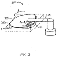
- Fig. 3 illustrates an apparatus 300 according to an embodiment of the present invention, comprising a conventional rotatable platen 310 for mounting a fixed abrasive article 320 to be conditioned.
- fixed abrasive article 320 comprises abrasive projections having different heights and upper-surface textures adhered to a backing member and immobilized in a polymeric binder.
- Platen 310 can be round or can be a square web 310a, as shown by the dotted lines, according to the shape of the abrasive article to be conditioned.
- Apparatus 300 further comprises a pivot arm 330, a holder or conditioning head 340 mounted to one end of pivot arm 330, and an abrasive disk 350 mounted to the underside of conditioning head 340.
- abrasive disk 350 can comprise a material having a roughness ⁇ 0.20 ⁇ m, such as silicon carbide, alumina, silica, titania, copper, resist, and polymers.
- Pivot arm 330 is operatively coupled to platen 310, and maintains conditioning head 340 and abrasive disk 350 against abrasive article 320.
- apparatus 300 is part of a chemical-mechanical polishing system and may comprise, for example, a chemical-mechanical polishing machine having a polishing head adapted to press a wafer against the abrasive article 320 to polish the wafer.
- abrasive article 320 is placed on platen 310 or 310a, and abrasive disk 350 is placed on conditioning head 340.
- Platen 310, 310a rotates as indicated by arrow B
- conditioning head 340 rotates as indicated by arrow C to scan a circular zone of abrasive article 320 to substantially equalize the textures and heights of the upper surfaces of the projections of abrasive article 320, as discussed above.
- pivot arm 330 scans back and forth across platen 310 as indicated by arrows A.
- apparatus 300 may include a rod 400 or similar elongated structural element extending from roughly from a center of the abrasive article 320 on the platen 310 to at least an outer diameter of the abrasive article 320.
- the rod 400 includes, on a surface corresponding to the abrasive article 320, a material having a roughness ⁇ 0.20 ⁇ m 320, such as silicon carbide, alumina, silica, copper, resist, and polymers.
- the rod is pressed against the abrasive article to condition the abrasive article 320 as the platen 310 rotates.
Applications Claiming Priority (2)
| Application Number | Priority Date | Filing Date | Title |
|---|---|---|---|
| US13217599P | 1999-05-03 | 1999-05-03 | |
| US132175P | 1999-05-03 |
Publications (1)
| Publication Number | Publication Date |
|---|---|
| EP1052062A1 true EP1052062A1 (de) | 2000-11-15 |
Family
ID=22452823
Family Applications (1)
| Application Number | Title | Priority Date | Filing Date |
|---|---|---|---|
| EP00303717A Withdrawn EP1052062A1 (de) | 1999-05-03 | 2000-05-03 | Vorbehandlung eines fixierten Schleifmittels |
Country Status (4)
| Country | Link |
|---|---|
| US (1) | US7014538B2 (de) |
| EP (1) | EP1052062A1 (de) |
| JP (1) | JP2001062701A (de) |
| KR (1) | KR20010020807A (de) |
Cited By (1)
| Publication number | Priority date | Publication date | Assignee | Title |
|---|---|---|---|---|
| DE10131668A1 (de) * | 2001-06-29 | 2003-01-30 | Infineon Technologies Ag | Verfahren zur abrasiven Bearbeitung von Oberflächen, insbesondere von Halbleiter-Wafern |
Families Citing this family (40)
| Publication number | Priority date | Publication date | Assignee | Title |
|---|---|---|---|---|
| US20050092621A1 (en) * | 2000-02-17 | 2005-05-05 | Yongqi Hu | Composite pad assembly for electrochemical mechanical processing (ECMP) |
| US20040020789A1 (en) * | 2000-02-17 | 2004-02-05 | Applied Materials, Inc. | Conductive polishing article for electrochemical mechanical polishing |
| US6991528B2 (en) * | 2000-02-17 | 2006-01-31 | Applied Materials, Inc. | Conductive polishing article for electrochemical mechanical polishing |
| US6962524B2 (en) * | 2000-02-17 | 2005-11-08 | Applied Materials, Inc. | Conductive polishing article for electrochemical mechanical polishing |
| US7125477B2 (en) * | 2000-02-17 | 2006-10-24 | Applied Materials, Inc. | Contacts for electrochemical processing |
| US7374644B2 (en) * | 2000-02-17 | 2008-05-20 | Applied Materials, Inc. | Conductive polishing article for electrochemical mechanical polishing |
| US7303662B2 (en) * | 2000-02-17 | 2007-12-04 | Applied Materials, Inc. | Contacts for electrochemical processing |
| US7678245B2 (en) * | 2000-02-17 | 2010-03-16 | Applied Materials, Inc. | Method and apparatus for electrochemical mechanical processing |
| US7029365B2 (en) * | 2000-02-17 | 2006-04-18 | Applied Materials Inc. | Pad assembly for electrochemical mechanical processing |
| US7670468B2 (en) * | 2000-02-17 | 2010-03-02 | Applied Materials, Inc. | Contact assembly and method for electrochemical mechanical processing |
| US7077721B2 (en) * | 2000-02-17 | 2006-07-18 | Applied Materials, Inc. | Pad assembly for electrochemical mechanical processing |
| US7137879B2 (en) * | 2001-04-24 | 2006-11-21 | Applied Materials, Inc. | Conductive polishing article for electrochemical mechanical polishing |
| US7344432B2 (en) * | 2001-04-24 | 2008-03-18 | Applied Materials, Inc. | Conductive pad with ion exchange membrane for electrochemical mechanical polishing |
| US20050194681A1 (en) * | 2002-05-07 | 2005-09-08 | Yongqi Hu | Conductive pad with high abrasion |
| JP4641781B2 (ja) * | 2003-11-04 | 2011-03-02 | 三星電子株式会社 | 不均一強度を有する研磨面を使用した化学的機械的研磨装置および方法 |
| US20060030156A1 (en) * | 2004-08-05 | 2006-02-09 | Applied Materials, Inc. | Abrasive conductive polishing article for electrochemical mechanical polishing |
| WO2006039436A2 (en) * | 2004-10-01 | 2006-04-13 | Applied Materials, Inc. | Pad design for electrochemical mechanical polishing |
| US7520968B2 (en) * | 2004-10-05 | 2009-04-21 | Applied Materials, Inc. | Conductive pad design modification for better wafer-pad contact |
| US7427340B2 (en) * | 2005-04-08 | 2008-09-23 | Applied Materials, Inc. | Conductive pad |
| US7179159B2 (en) * | 2005-05-02 | 2007-02-20 | Applied Materials, Inc. | Materials for chemical mechanical polishing |
| US20070153453A1 (en) * | 2006-01-05 | 2007-07-05 | Applied Materials, Inc. | Fully conductive pad for electrochemical mechanical processing |
| US20070235344A1 (en) * | 2006-04-06 | 2007-10-11 | Applied Materials, Inc. | Process for high copper removal rate with good planarization and surface finish |
| US20070243798A1 (en) * | 2006-04-18 | 2007-10-18 | 3M Innovative Properties Company | Embossed structured abrasive article and method of making and using the same |
| US7410413B2 (en) * | 2006-04-27 | 2008-08-12 | 3M Innovative Properties Company | Structured abrasive article and method of making and using the same |
| US20070251832A1 (en) * | 2006-04-27 | 2007-11-01 | Applied Materials, Inc. | Method and apparatus for electrochemical mechanical polishing of cu with higher liner velocity for better surface finish and higher removal rate during clearance |
| US20070272674A1 (en) * | 2006-05-26 | 2007-11-29 | 3M Innovative Properties Company | Abrasive brush recovery system and process |
| US7963827B2 (en) * | 2006-07-14 | 2011-06-21 | Saint-Gobain Abrastives, Inc. | Backingless abrasive article |
| US8012000B2 (en) * | 2007-04-02 | 2011-09-06 | Applied Materials, Inc. | Extended pad life for ECMP and barrier removal |
| US20080293343A1 (en) * | 2007-05-22 | 2008-11-27 | Yuchun Wang | Pad with shallow cells for electrochemical mechanical processing |
| DE112008001866T5 (de) * | 2007-07-27 | 2010-07-22 | Saint-Gobain Abrasifs | Automatische Detektion von Charakteristiken von Schleifmittelprodukten während der Verwendung |
| CN102105266B (zh) * | 2008-06-13 | 2016-01-13 | 福吉米株式会社 | 氧化铝颗粒以及包含该氧化铝颗粒的抛光组合物 |
| US8439723B2 (en) * | 2008-08-11 | 2013-05-14 | Applied Materials, Inc. | Chemical mechanical polisher with heater and method |
| KR101177497B1 (ko) * | 2009-07-01 | 2012-08-27 | 서강대학교산학협력단 | 기공이 형성된 cmp 연마패드 및 기공의 형성방법 |
| JP5428793B2 (ja) * | 2009-11-17 | 2014-02-26 | 旭硝子株式会社 | ガラス基板研磨方法および磁気記録媒体用ガラス基板の製造方法 |
| CA2784902A1 (en) * | 2009-12-29 | 2011-07-28 | Saint-Gobain Abrasives, Inc. | Method of cleaning a household surface |
| EP2455186A1 (de) * | 2010-11-17 | 2012-05-23 | Schneider GmbH & Co. KG | Vorrichtung und Verfahren zum Bearbeiten einer optischen Linse mit automatischer Identifizierung der optischen Linse |
| KR101211138B1 (ko) * | 2011-03-07 | 2012-12-11 | 이화다이아몬드공업 주식회사 | 연약패드용 컨디셔너 및 그 제조방법 |
| SG11201906131WA (en) | 2017-01-20 | 2019-08-27 | Applied Materials Inc | A thin plastic polishing article for cmp applications |
| US11717936B2 (en) | 2018-09-14 | 2023-08-08 | Applied Materials, Inc. | Methods for a web-based CMP system |
| WO2020128852A1 (en) * | 2018-12-18 | 2020-06-25 | 3M Innovative Properties Company | Patterned abrasive substrate and method |
Citations (5)
| Publication number | Priority date | Publication date | Assignee | Title |
|---|---|---|---|---|
| US5527424A (en) * | 1995-01-30 | 1996-06-18 | Motorola, Inc. | Preconditioner for a polishing pad and method for using the same |
| US5692950A (en) * | 1996-08-08 | 1997-12-02 | Minnesota Mining And Manufacturing Company | Abrasive construction for semiconductor wafer modification |
| WO1998039142A1 (en) * | 1997-03-07 | 1998-09-11 | Minnesota Mining And Manufacturing Company | Abrasive article for providing a clear surface finish on glass |
| US5810964A (en) * | 1995-12-06 | 1998-09-22 | Nec Corporation | Chemical mechanical polishing device for a semiconductor wafer |
| WO1998045090A1 (en) * | 1997-04-04 | 1998-10-15 | Obsidian, Inc. | Polishing media magazine for improved polishing |
Family Cites Families (155)
| Publication number | Priority date | Publication date | Assignee | Title |
|---|---|---|---|---|
| BE333311A (de) | 1925-05-23 | |||
| US1927162A (en) | 1931-02-27 | 1933-09-19 | Research Corp | Electroplating |
| US2112691A (en) | 1936-01-30 | 1938-03-29 | Pyrene Mfg Co | Electroplating anode unit |
| US2240265A (en) | 1937-03-30 | 1941-04-29 | John S Nachtman | Method of continuously tin plating ferrous metal stock |
| US2431065A (en) | 1938-12-12 | 1947-11-18 | Meaker Company | Continuous wire and strip electro-processing machine |
| US2392687A (en) | 1943-02-15 | 1946-01-08 | John S Nachtman | Apparatus for electroplating wire |
| US2461556A (en) | 1943-04-01 | 1949-02-15 | Carnegie Illinois Steel Corp | Method and apparatus for the electrolytic coating of metal strip |
| US2544510A (en) | 1943-10-23 | 1951-03-06 | Nat Steel Corp | Apparatus and method for plating strips |
| US2503863A (en) | 1943-11-18 | 1950-04-11 | Siegfried G Bart | Apparatus for electroplating the inside of pipes |
| US2509304A (en) | 1944-02-24 | 1950-05-30 | Nat Steel Corp | Method and apparatus for electrolytic coating of strip material |
| US2453481A (en) | 1944-03-14 | 1948-11-09 | Nat Steel Corp | Anode for electrolytic coating |
| US2490055A (en) | 1944-03-30 | 1949-12-06 | Nat Steel Corp | Metal strip electroplating apparatus |
| US2495695A (en) | 1944-05-08 | 1950-01-31 | Kenmore Metals Corp | Electroplating apparatus |
| US2536912A (en) | 1944-07-12 | 1951-01-02 | Ibm | Electrolysis etching device |
| US2569578A (en) | 1944-08-07 | 1951-10-02 | Nat Steel Corp | Apparatus for electrocoating striplike material |
| US2480022A (en) | 1944-10-07 | 1949-08-23 | George B Hogaboom | Rotary barrel |
| US2473290A (en) | 1944-10-21 | 1949-06-14 | George E Millard | Apparatus for plating journals of crankshafts |
| US2456185A (en) | 1944-11-23 | 1948-12-14 | Gen Motors Corp | Electroplating apparatus |
| US2517907A (en) | 1945-01-05 | 1950-08-08 | Conmar Prod Corp | Apparatus for electrotreating metal slide fasteners |
| US2500205A (en) | 1945-04-12 | 1950-03-14 | Cleveland Graphite Bronze Co | Method of plating |
| US2454935A (en) | 1945-06-27 | 1948-11-30 | Meaker Company | Continuous wire and strip electroprocessing machine |
| NL69965C (de) | 1945-08-10 | |||
| US2619454A (en) | 1945-08-30 | 1952-11-25 | Brush Dev Co | Method of manufacturing a magnetic recording medium by electrodeposition |
| US2554943A (en) | 1945-10-25 | 1951-05-29 | Bethlehem Steel Corp | Electroplating apparatus |
| US2506794A (en) | 1945-11-23 | 1950-05-09 | Revere Copper & Brass Inc | Apparatus for electroplating |
| US2530677A (en) | 1946-01-17 | 1950-11-21 | Edward L Berkenkotter | Apparatus for plating crankshafts |
| US2457510A (en) | 1946-01-23 | 1948-12-28 | Delbert G Van Ornum | Electroplating apparatus |
| US2519945A (en) | 1946-01-25 | 1950-08-22 | Gen Electric | Electroplating apparatus |
| US2477808A (en) | 1946-05-08 | 1949-08-02 | Carl G Jones | Electrolytic apparatus for treatment of moving strip |
| US2576074A (en) | 1946-06-11 | 1951-11-20 | John S Nachtman | Method and apparatus for continuous strip metal treatment |
| US2479323A (en) | 1946-06-13 | 1949-08-16 | Udylite Corp | Plating machine |
| US2512328A (en) | 1946-06-28 | 1950-06-20 | Armco Steel Corp | Continuous electroplating device |
| US2500206A (en) | 1946-06-29 | 1950-03-14 | Cleveland Graphite Bronze Co | Apparatus for plating |
| US2560534A (en) | 1946-07-12 | 1951-07-17 | Nat Standard Co | Method of operating a continuous electroplating system |
| US2539898A (en) | 1946-08-16 | 1951-01-30 | Udylite Corp | Electrical contact mechanism for plating machines |
| US2549678A (en) | 1946-08-23 | 1951-04-17 | Conn Ltd C G | Method of and apparatus for electroforming metal articles |
| US2556017A (en) | 1947-01-29 | 1951-06-05 | Edwin E Vonada | Electrolytic method and apparatus for cleaning strip |
| US2535966A (en) | 1947-02-07 | 1950-12-26 | Teplitz Alfred | Electrolytic apparatus for cleaning strip |
| US2540175A (en) | 1947-02-11 | 1951-02-06 | Rosenqvist Gunnar | Manufacture by electrodeposition |
| US2569577A (en) | 1947-05-09 | 1951-10-02 | Nat Steel Corp | Method of and apparatus for electroplating |
| US2458676A (en) | 1947-07-22 | 1949-01-11 | Brenner Abner | Apparatus for electroplating |
| US2560966A (en) | 1947-07-31 | 1951-07-17 | Revere Copper & Brass Inc | Method of electroplating copper clad stainless steel cooking vessels |
| US2571709A (en) | 1947-08-26 | 1951-10-16 | Western Electric Co | Apparatus for electroplating articles |
| US2646398A (en) | 1948-10-08 | 1953-07-21 | Gen Motors Corp | Electroprocessing apparatus |
| BE494578A (de) | 1949-03-18 | |||
| US2689215A (en) | 1949-07-13 | 1954-09-14 | Siegfried G Bart | Method and apparatus for plating pipe |
| US2587630A (en) | 1949-07-28 | 1952-03-04 | Sulphide Ore Process Company I | Method for electrodeposition of iron in the form of continuous strips |
| US2656283A (en) | 1949-08-31 | 1953-10-20 | Ohio Commw Eng Co | Method of plating wire |
| US2656284A (en) | 1949-09-07 | 1953-10-20 | Ohio Commw Eng Co | Method of plating rolled sheet metal |
| US2657457A (en) | 1949-09-10 | 1953-11-03 | Ohio Commw Eng Co | Continuous metal production and continuous gas plating |
| US2684939A (en) | 1949-12-17 | 1954-07-27 | Time Inc | Apparatus for plating chromium |
| US2633452A (en) | 1950-05-03 | 1953-03-31 | Jr George B Hogaboom | Strainer bags for enclosing electroplating anodes |
| US2657177A (en) | 1950-07-10 | 1953-10-27 | United States Steel Corp | Plating thickness regulator |
| US2674550A (en) | 1950-09-05 | 1954-04-06 | Kolene Corp | Apparatus and method for processing of steel strip continuously |
| US2680710A (en) | 1950-09-14 | 1954-06-08 | Kenmore Metal Corp | Method and apparatus for continuously electroplating heavy wire and similar strip material |
| US2675348A (en) | 1950-09-16 | 1954-04-13 | Greenspan Lawrence | Apparatus for metal plating |
| US2686859A (en) | 1950-10-11 | 1954-08-17 | Western Electric Co | Electroplating |
| US2706173A (en) | 1950-10-12 | 1955-04-12 | Harold R Wells | Apparatus for electro-plating crankshaft journals |
| US2673836A (en) | 1950-11-22 | 1954-03-30 | United States Steel Corp | Continuous electrolytic pickling and tin plating of steel strip |
| US2695269A (en) | 1951-03-02 | 1954-11-23 | United States Steel Corp | Apparatus for electroplating wire |
| US2698832A (en) | 1951-03-20 | 1955-01-04 | Standard Process Corp | Plating apparatus |
| US2711993A (en) | 1951-05-01 | 1955-06-28 | Lyon George Albert | Apparatus for conveying cylindrical articles through a bath |
| US2710834A (en) | 1951-10-27 | 1955-06-14 | Vrilakas Marcus | Apparatus for selective plating |
| US2708445A (en) | 1952-07-11 | 1955-05-17 | Nat Standard Co | Wire processing apparatus |
| US3162588A (en) | 1961-04-17 | 1964-12-22 | Hammond Machinery Builders Inc | Belt type electrolytic grinding machine |
| US3334041A (en) * | 1964-08-28 | 1967-08-01 | Norton Co | Coated abrasives |
| US3476677A (en) | 1965-02-15 | 1969-11-04 | Carbond Corp | Electrolytic grinding tools |
| US3433730A (en) | 1965-04-28 | 1969-03-18 | Gen Electric | Electrically conductive tool and method for making |
| US3448023A (en) | 1966-01-20 | 1969-06-03 | Hammond Machinery Builders Inc | Belt type electro-chemical (or electrolytic) grinding machine |
| US3942959A (en) * | 1967-12-22 | 1976-03-09 | Fabriksaktiebolaget Eka | Multilayered flexible abrasive containing a layer of electroconductive material |
| AU3308268A (en) | 1968-02-05 | 1970-03-12 | Raynors Pty. Limited | Plating and anodising bath racks |
| US3992178A (en) * | 1973-04-17 | 1976-11-16 | Fabrika Ab Eka | Flexible coated abrasive with graphite outer layer |
| US3873512A (en) | 1973-04-30 | 1975-03-25 | Martin Marietta Corp | Machining method |
| US4001094A (en) | 1974-09-19 | 1977-01-04 | Jumer John F | Method for incremental electro-processing of large areas |
| US4047902A (en) | 1975-04-01 | 1977-09-13 | Wiand Richard K | Metal-plated abrasive product and method of manufacturing the product |
| GB1539309A (en) | 1976-12-14 | 1979-01-31 | Inoue Japax Res | Electrochemical polishing |
| US4119515A (en) | 1977-03-28 | 1978-10-10 | National Steel Corporation | Apparatus for electroplating sheet metals |
| US4312716A (en) | 1980-11-21 | 1982-01-26 | Western Electric Co., Inc. | Supporting an array of elongate articles |
| US4523411A (en) | 1982-12-20 | 1985-06-18 | Minnesota Mining And Manufacturing Company | Wet surface treating device and element therefor |
| JPS61265279A (ja) * | 1985-05-17 | 1986-11-25 | Tohoku Metal Ind Ltd | フレキシブル磁気デイスク用研摩テ−プ |
| US4704511A (en) | 1985-10-17 | 1987-11-03 | Inoue-Japax Research Incorporated | Traveling-wire electroerosion machine with swiveling nozzle assembly |
| JPS62127492A (ja) | 1985-11-26 | 1987-06-09 | Shigeo Hoshino | カ−ボン繊維を用いる電気めつきの方法 |
| US4839993A (en) | 1986-01-28 | 1989-06-20 | Fujisu Limited | Polishing machine for ferrule of optical fiber connector |
| ES2024439B3 (es) | 1986-02-28 | 1992-03-01 | Schering Ag Berlin Und Bergkamen | Armazones alargados y piezas correspondientes para la fijacion soltable de placas de circuito impreso que han de galvanizarse, y placas de circuito impreso correspondientes. |
| US4772361A (en) | 1987-12-04 | 1988-09-20 | Dorsett Terry E | Application of electroplate to moving metal by belt plating |
| US4793895A (en) | 1988-01-25 | 1988-12-27 | Ibm Corporation | In situ conductivity monitoring technique for chemical/mechanical planarization endpoint detection |
| JPH01193166A (ja) | 1988-01-28 | 1989-08-03 | Showa Denko Kk | 半導体ウェハ鏡面研磨用パッド |
| US4934102A (en) | 1988-10-04 | 1990-06-19 | International Business Machines Corporation | System for mechanical planarization |
| JP2601333B2 (ja) | 1988-10-05 | 1997-04-16 | 三井金属鉱業株式会社 | 複合砥石およびその製造方法 |
| CH678156A5 (de) | 1989-03-20 | 1991-08-15 | Exnii Metallorezh Stankov | |
| US5014468A (en) | 1989-05-05 | 1991-05-14 | Norton Company | Patterned coated abrasive for fine surface finishing |
| US5061294A (en) * | 1989-05-15 | 1991-10-29 | Minnesota Mining And Manufacturing Company | Abrasive article with conductive, doped, conjugated, polymer coat and method of making same |
| US5108463B1 (en) * | 1989-08-21 | 1996-08-13 | Minnesota Mining & Mfg | Conductive coated abrasives |
| US5136817A (en) | 1990-02-28 | 1992-08-11 | Nihon Dempa Kogyo Co., Ltd. | Automatic lapping apparatus for piezoelectric materials |
| US5257478A (en) | 1990-03-22 | 1993-11-02 | Rodel, Inc. | Apparatus for interlayer planarization of semiconductor material |
| US5137542A (en) | 1990-08-08 | 1992-08-11 | Minnesota Mining And Manufacturing Company | Abrasive printed with an electrically conductive ink |
| US5066370A (en) | 1990-09-07 | 1991-11-19 | International Business Machines Corporation | Apparatus, electrochemical process, and electrolyte for microfinishing stainless steel print bands |
| US5096550A (en) | 1990-10-15 | 1992-03-17 | The United States Of America As Represented By The United States Department Of Energy | Method and apparatus for spatially uniform electropolishing and electrolytic etching |
| US5152917B1 (en) | 1991-02-06 | 1998-01-13 | Minnesota Mining & Mfg | Structured abrasive article |
| US5217586A (en) | 1992-01-09 | 1993-06-08 | International Business Machines Corporation | Electrochemical tool for uniform metal removal during electropolishing |
| US5437754A (en) | 1992-01-13 | 1995-08-01 | Minnesota Mining And Manufacturing Company | Abrasive article having precise lateral spacing between abrasive composite members |
| BR9305871A (pt) * | 1992-02-12 | 1997-08-19 | Minnesota Mining & Mfg | Artigo abrasivo revestido e processo para sua fabricação |
| JPH05277957A (ja) * | 1992-04-02 | 1993-10-26 | Nippon Micro Kooteingu Kk | 帯電防止研磨シート |
| US5225034A (en) | 1992-06-04 | 1993-07-06 | Micron Technology, Inc. | Method of chemical mechanical polishing predominantly copper containing metal layers in semiconductor processing |
| US5203884A (en) * | 1992-06-04 | 1993-04-20 | Minnesota Mining And Manufacturing Company | Abrasive article having vanadium oxide incorporated therein |
| US5328716A (en) | 1992-08-11 | 1994-07-12 | Minnesota Mining And Manufacturing Company | Method of making a coated abrasive article containing a conductive backing |
| US5562529A (en) * | 1992-10-08 | 1996-10-08 | Fujitsu Limited | Apparatus and method for uniformly polishing a wafer |
| US5542032A (en) * | 1993-10-04 | 1996-07-30 | Loral Federal Systems Company | Fast display of images of three-dimensional surfaces without aliasing |
| US5453312A (en) | 1993-10-29 | 1995-09-26 | Minnesota Mining And Manufacturing Company | Abrasive article, a process for its manufacture, and a method of using it to reduce a workpiece surface |
| US5454844A (en) | 1993-10-29 | 1995-10-03 | Minnesota Mining And Manufacturing Company | Abrasive article, a process of making same, and a method of using same to finish a workpiece surface |
| US5534106A (en) * | 1994-07-26 | 1996-07-09 | Kabushiki Kaisha Toshiba | Apparatus for processing semiconductor wafers |
| JPH08112769A (ja) * | 1994-10-14 | 1996-05-07 | Fuji Photo Film Co Ltd | 研磨テープ |
| US6017265A (en) * | 1995-06-07 | 2000-01-25 | Rodel, Inc. | Methods for using polishing pads |
| US5893796A (en) * | 1995-03-28 | 1999-04-13 | Applied Materials, Inc. | Forming a transparent window in a polishing pad for a chemical mechanical polishing apparatus |
| US6024630A (en) * | 1995-06-09 | 2000-02-15 | Applied Materials, Inc. | Fluid-pressure regulated wafer polishing head |
| US5702811A (en) * | 1995-10-20 | 1997-12-30 | Ho; Kwok-Lun | High performance abrasive articles containing abrasive grains and nonabrasive composite grains |
| US5738574A (en) * | 1995-10-27 | 1998-04-14 | Applied Materials, Inc. | Continuous processing system for chemical mechanical polishing |
| US5882491A (en) * | 1996-01-02 | 1999-03-16 | Skf Industrial Trading & Development Company B.V. | Electrode for electrochemical machining, method of electrochemical machining with said electrode, a bearing and a method of determining a profile using said electrode |
| NL1003233C2 (nl) * | 1996-05-30 | 1997-12-03 | Skf Ind Trading & Dev | Werkwijze voor het vervaardigen van een lagerring en een lager dat een dergelijke lagerring omvat. |
| US5871392A (en) * | 1996-06-13 | 1999-02-16 | Micron Technology, Inc. | Under-pad for chemical-mechanical planarization of semiconductor wafers |
| US6056851A (en) * | 1996-06-24 | 2000-05-02 | Taiwan Semiconductor Manufacturing Company | Slurry supply system for chemical mechanical polishing |
| US6183354B1 (en) * | 1996-11-08 | 2001-02-06 | Applied Materials, Inc. | Carrier head with a flexible membrane for a chemical mechanical polishing system |
| US6020264A (en) * | 1997-01-31 | 2000-02-01 | International Business Machines Corporation | Method and apparatus for in-line oxide thickness determination in chemical-mechanical polishing |
| US5911619A (en) * | 1997-03-26 | 1999-06-15 | International Business Machines Corporation | Apparatus for electrochemical mechanical planarization |
| US6537140B1 (en) * | 1997-05-14 | 2003-03-25 | Saint-Gobain Abrasives Technology Company | Patterned abrasive tools |
| JPH1158205A (ja) * | 1997-08-25 | 1999-03-02 | Unique Technol Internatl Pte Ltd | 電解研磨併用ポリシング・テクスチャー加工装置および加工方法ならびにそれに使用する電解研磨併用ポリシング・テクスチャーテープ |
| US6033293A (en) * | 1997-10-08 | 2000-03-07 | Lucent Technologies Inc. | Apparatus for performing chemical-mechanical polishing |
| US6372001B1 (en) * | 1997-10-09 | 2002-04-16 | 3M Innovative Properties Company | Abrasive articles and their preparations |
| US6171467B1 (en) * | 1997-11-25 | 2001-01-09 | The John Hopkins University | Electrochemical-control of abrasive polishing and machining rates |
| KR100474746B1 (ko) * | 1998-02-12 | 2005-03-08 | 에이씨엠 리서치, 인코포레이티드 | 도금 장치 및 방법 |
| US6004880A (en) * | 1998-02-20 | 1999-12-21 | Lsi Logic Corporation | Method of single step damascene process for deposition and global planarization |
| US6210257B1 (en) * | 1998-05-29 | 2001-04-03 | Micron Technology, Inc. | Web-format polishing pads and methods for manufacturing and using web-format polishing pads in mechanical and chemical-mechanical planarization of microelectronic substrates |
| US6395152B1 (en) * | 1998-07-09 | 2002-05-28 | Acm Research, Inc. | Methods and apparatus for electropolishing metal interconnections on semiconductor devices |
| US6190494B1 (en) * | 1998-07-29 | 2001-02-20 | Micron Technology, Inc. | Method and apparatus for electrically endpointing a chemical-mechanical planarization process |
| US6176992B1 (en) * | 1998-11-03 | 2001-01-23 | Nutool, Inc. | Method and apparatus for electro-chemical mechanical deposition |
| JP2000141215A (ja) * | 1998-11-05 | 2000-05-23 | Sony Corp | 平坦化研磨装置及び平坦化研磨方法 |
| US6251235B1 (en) * | 1999-03-30 | 2001-06-26 | Nutool, Inc. | Apparatus for forming an electrical contact with a semiconductor substrate |
| US6328872B1 (en) * | 1999-04-03 | 2001-12-11 | Nutool, Inc. | Method and apparatus for plating and polishing a semiconductor substrate |
| US6409904B1 (en) * | 1998-12-01 | 2002-06-25 | Nutool, Inc. | Method and apparatus for depositing and controlling the texture of a thin film |
| US6077337A (en) * | 1998-12-01 | 2000-06-20 | Intel Corporation | Chemical-mechanical polishing slurry |
| US6244935B1 (en) * | 1999-02-04 | 2001-06-12 | Applied Materials, Inc. | Apparatus and methods for chemical mechanical polishing with an advanceable polishing sheet |
| US6066030A (en) * | 1999-03-04 | 2000-05-23 | International Business Machines Corporation | Electroetch and chemical mechanical polishing equipment |
| US6238592B1 (en) * | 1999-03-10 | 2001-05-29 | 3M Innovative Properties Company | Working liquids and methods for modifying structured wafers suited for semiconductor fabrication |
| US6217426B1 (en) * | 1999-04-06 | 2001-04-17 | Applied Materials, Inc. | CMP polishing pad |
| US6238271B1 (en) * | 1999-04-30 | 2001-05-29 | Speed Fam-Ipec Corp. | Methods and apparatus for improved polishing of workpieces |
| US6244222B1 (en) * | 1999-05-12 | 2001-06-12 | Els Blok Bowen | Adjustable pet collars |
| US6381169B1 (en) * | 1999-07-01 | 2002-04-30 | The Regents Of The University Of California | High density non-volatile memory device |
| US6234870B1 (en) * | 1999-08-24 | 2001-05-22 | International Business Machines Corporation | Serial intelligent electro-chemical-mechanical wafer processor |
| US6406363B1 (en) * | 1999-08-31 | 2002-06-18 | Lam Research Corporation | Unsupported chemical mechanical polishing belt |
| US6368184B1 (en) * | 2000-01-06 | 2002-04-09 | Advanced Micro Devices, Inc. | Apparatus for determining metal CMP endpoint using integrated polishing pad electrodes |
| US6368190B1 (en) * | 2000-01-26 | 2002-04-09 | Agere Systems Guardian Corp. | Electrochemical mechanical planarization apparatus and method |
| US6402591B1 (en) * | 2000-03-31 | 2002-06-11 | Lam Research Corporation | Planarization system for chemical-mechanical polishing |
| US6383066B1 (en) * | 2000-06-23 | 2002-05-07 | International Business Machines Corporation | Multilayered polishing pad, method for fabricating, and use thereof |
| US6257953B1 (en) * | 2000-09-25 | 2001-07-10 | Center For Tribology, Inc. | Method and apparatus for controlled polishing |
| US20030013397A1 (en) * | 2001-06-27 | 2003-01-16 | Rhoades Robert L. | Polishing pad of polymer coating |
-
2000
- 2000-05-03 EP EP00303717A patent/EP1052062A1/de not_active Withdrawn
- 2000-05-03 KR KR1020000023670A patent/KR20010020807A/ko not_active Application Discontinuation
- 2000-05-08 JP JP2000134966A patent/JP2001062701A/ja not_active Withdrawn
-
2003
- 2003-03-05 US US10/382,079 patent/US7014538B2/en not_active Expired - Fee Related
Patent Citations (5)
| Publication number | Priority date | Publication date | Assignee | Title |
|---|---|---|---|---|
| US5527424A (en) * | 1995-01-30 | 1996-06-18 | Motorola, Inc. | Preconditioner for a polishing pad and method for using the same |
| US5810964A (en) * | 1995-12-06 | 1998-09-22 | Nec Corporation | Chemical mechanical polishing device for a semiconductor wafer |
| US5692950A (en) * | 1996-08-08 | 1997-12-02 | Minnesota Mining And Manufacturing Company | Abrasive construction for semiconductor wafer modification |
| WO1998039142A1 (en) * | 1997-03-07 | 1998-09-11 | Minnesota Mining And Manufacturing Company | Abrasive article for providing a clear surface finish on glass |
| WO1998045090A1 (en) * | 1997-04-04 | 1998-10-15 | Obsidian, Inc. | Polishing media magazine for improved polishing |
Cited By (3)
| Publication number | Priority date | Publication date | Assignee | Title |
|---|---|---|---|---|
| DE10131668A1 (de) * | 2001-06-29 | 2003-01-30 | Infineon Technologies Ag | Verfahren zur abrasiven Bearbeitung von Oberflächen, insbesondere von Halbleiter-Wafern |
| US6824451B2 (en) | 2001-06-29 | 2004-11-30 | Infineon Technologies Ag | Process for the abrasive machining of surfaces, in particular of semiconductor wafers |
| DE10131668B4 (de) * | 2001-06-29 | 2006-05-18 | Infineon Technologies Ag | Verfahren zur abrasiven Bearbeitung von Oberflächen, auf Halbleiter-Wafern |
Also Published As
| Publication number | Publication date |
|---|---|
| KR20010020807A (ko) | 2001-03-15 |
| JP2001062701A (ja) | 2001-03-13 |
| US7014538B2 (en) | 2006-03-21 |
| US20040082288A1 (en) | 2004-04-29 |
Similar Documents
| Publication | Publication Date | Title |
|---|---|---|
| EP1052062A1 (de) | Vorbehandlung eines fixierten Schleifmittels | |
| EP0999013B1 (de) | Polierschleifscheibe und substrat polierverfahren mit hilfe dieser schleifscheibe | |
| US6241585B1 (en) | Apparatus and method for chemical mechanical polishing | |
| US6857941B2 (en) | Multi-phase polishing pad | |
| US20010029157A1 (en) | Polishing pads and planarizing machines for mechanical and/or chemical-mechanical planarization of microelectronic substrate assemblies | |
| JP4803863B2 (ja) | 固定研磨部材をコンディショニングする方法およびケミカルメカニカルポリシングのための方法 | |
| EP1238756A1 (de) | Chemisch-mechanisches Polierverfahren mit mehreren Poleirkissen | |
| US7021996B2 (en) | Apparatus and method for conditioning a contact surface of a processing pad used in processing microelectronic workpieces | |
| EP1034886B1 (de) | Poliereinrichtung enthaltend eine Einstellkontrolle für eine Abziehvorrichtung | |
| EP1066923A2 (de) | Trägerplatte mit einer abgeänderte flexiblen Membran | |
| US6420265B1 (en) | Method for polishing semiconductor device | |
| US20030013389A1 (en) | Process for the abrasive machining of surfaces, in particular of semiconductor wafers | |
| EP1322449B1 (de) | Abrichtvorrichtung für polierkissen und verfahren zu dessen anwendung | |
| US20020016136A1 (en) | Conditioner for polishing pads | |
| JP3528501B2 (ja) | 半導体の製造方法 | |
| US7175515B2 (en) | Static pad conditioner | |
| US6832948B1 (en) | Thermal preconditioning fixed abrasive articles | |
| KR20010040249A (ko) | 연마장치 및 그 장치를 사용한 반도체제조방법 | |
| JP2001088008A (ja) | 研磨方法とその装置 | |
| JP2005125420A (ja) | 連続研磨装置の研磨具のドレッシング方法 |
Legal Events
| Date | Code | Title | Description |
|---|---|---|---|
| PUAI | Public reference made under article 153(3) epc to a published international application that has entered the european phase |
Free format text: ORIGINAL CODE: 0009012 |
|
| AK | Designated contracting states |
Kind code of ref document: A1 Designated state(s): DE FR GB IT NL |
|
| AX | Request for extension of the european patent |
Free format text: AL;LT;LV;MK;RO;SI |
|
| RIN1 | Information on inventor provided before grant (corrected) |
Inventor name: WHITE, JOHN M. Inventor name: EMAMI, RAMIN Inventor name: BIRANG, MANOOCHER Inventor name: SCALES, MARTIN Inventor name: ROSENBERG, LAWRENCE M Inventor name: TIETZ, JAMES V. Inventor name: LI, SHIJIAN |
|
| RAP1 | Party data changed (applicant data changed or rights of an application transferred) |
Owner name: TODA KOGYO CORPORATION |
|
| 17P | Request for examination filed |
Effective date: 20010417 |
|
| RAP1 | Party data changed (applicant data changed or rights of an application transferred) |
Owner name: APPLIED MATERIALS, INC. |
|
| AKX | Designation fees paid |
Free format text: DE FR GB IT NL |
|
| STAA | Information on the status of an ep patent application or granted ep patent |
Free format text: STATUS: THE APPLICATION IS DEEMED TO BE WITHDRAWN |
|
| 18D | Application deemed to be withdrawn |
Effective date: 20021203 |