EP1049021B1 - Sequential bus architecture - Google Patents
Sequential bus architecture Download PDFInfo
- Publication number
- EP1049021B1 EP1049021B1 EP00303602A EP00303602A EP1049021B1 EP 1049021 B1 EP1049021 B1 EP 1049021B1 EP 00303602 A EP00303602 A EP 00303602A EP 00303602 A EP00303602 A EP 00303602A EP 1049021 B1 EP1049021 B1 EP 1049021B1
- Authority
- EP
- European Patent Office
- Prior art keywords
- transaction
- modules
- bus
- module
- address
- Prior art date
- Legal status (The legal status is an assumption and is not a legal conclusion. Google has not performed a legal analysis and makes no representation as to the accuracy of the status listed.)
- Expired - Lifetime
Links
Images


Classifications
-
- G—PHYSICS
- G06—COMPUTING OR CALCULATING; COUNTING
- G06F—ELECTRIC DIGITAL DATA PROCESSING
- G06F13/00—Interconnection of, or transfer of information or other signals between, memories, input/output devices or central processing units
- G06F13/38—Information transfer, e.g. on bus
- G06F13/42—Bus transfer protocol, e.g. handshake; Synchronisation
- G06F13/4247—Bus transfer protocol, e.g. handshake; Synchronisation on a daisy chain bus
- G06F13/4256—Bus transfer protocol, e.g. handshake; Synchronisation on a daisy chain bus using a clocked protocol
Definitions
- the present invention relates to bus architectures and, in particular, to a sequential arrangement which consumes minimal space when implemented in hardware, particularly in integrated applications.
- bus architectures have been developed over the years to handle a variety of situations which require the communication of information between individual devices and/or modules in electronic systems.
- the extent to which certain bus architectures are utilised depends upon a number of factors including the rate of data transfer required to be implemented by the bus, the particular environment in which data transfer is being conducted, and the distance over which data must be transferred.
- buses are formed typically by parallel bi-directional arrangements controlled by a microprocessor type device.
- a serial bus may be coupled to a number of devices or modules which relies upon the individual module sensing the availability of the interconnection between the modules and capturing control of the communication link at the time data transmission is available.
- the integrated device may include a number of modules with which communications is desired, such communications being channelled through a single external interface port associated with the integrated device.
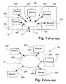
- An arrangement such as this is shown in Fig. 1 where a single integrated device 10 is shown illustrated which includes a communication module 12 located at or near a periphery of the device 10 and to which an external communication link 14 connects. Within the device 10 are a plurality of modules 16A-16E with which data from the communication link 14 is desired to be transferred.
- the communications module 12 includes a number of communications links 18A-18E to the respective modules 16A-16E which provide for the multiplexing of communication signals to the intended module 16A-16E.
- the links 18A-18E typically comprise a parallel bus arrangement. Where an arrangement similar to Fig.
- FIG. 1 is implemented in a printed circuit or larger scale application, such an arrangement presents little problem to the electronics designer in terms of the specifics of implementing the various communication links around the printed circuit card or system.
- problems arise where the number of individual modules 16 becomes large, thus necessitating a correspondingly large number of links 18.
- the modules 16 are spread about the integrated device, it becomes architecturally difficult for the integrated circuit designer to provide for the various integrated and wire connections between the modules 16 and the communication interface module 12. There is also insufficient room on the integrated circuit in the vicinity of the module 12 to allow for convenience and/or economic placement of the communication links.
- a communications arrangement 20 is provided incorporating a ring-bus which interconnects a plurality of modules 24A-24F, each having corresponding connections 26A-26F to the bus 22.
- any one of the modules 24A-24F can be configured for communications to an external arrangement and thus the arrangement 20 may be used in both printed circuit and integrated applications.
- Such an arrangement requires the implementation of tri-state logic to allow coupling to the ring bus 22.
- the arrangement of Fig. 2 becomes problematic, particularly in integrated applications, as the ring bus 22 is required to have connected to it a number of modules all representing varying loads and this may result in transmission problems within the device resulting in difficulties in resolving conflicts such as those mentioned above.
- US Patent No. 4,916,647 discloses a computer having a ring-bus connecting a number of independent processor modules, similar to the type shown in Fig. 2 of the present application.
- a bus architecture for a system comprising a plurality of modules with which communication is desired via an access port of said system according to claim 1.
- a computer graphics co-processor integrated circuit device comprising an internal bus architecture according to the first aspect of the present invention.
- an integrated circuit device incorporating a bus architecture according to the first aspect of the present invention.
- Fig. 3 illustrates the bus architecture system in accordance with an embodiment of the present invention formed within a integrated circuit device 30 having a communications port 34 configured to permit interface with electronics systems not illustrated.
- the port 34 connects to a communications module 32 forming part of a sequential bus arrangement incorporating a number of modules 36A-36E of the device 30 and a number of uni-directional interconnections 38A-38F arranged between sequential ones of those modules 36A-36E.
- the device 30 may include a number of further connections external and internal to the device 30 that connect to the various modules 36A-36E.
- communication signals received by the communication module 32 include both data and address components, the address component, being an address of or within an intended one of the modules 36A-36E to which the data is to be applied and/or used.
- the module 32 instigates the transfer of the communication transaction around the sequential bus, with each module 36 examining the intended address carried by the transaction to determine whether or not the data is intended for that particular module 36, and if not, being responsible for the transfer of the communication transaction to the next module until such time as the communication transaction is received by the destination module.
- any one of the modules 36A-36E can transmit a data package onto the bus in a similar fashion where it may be used by any of the other modules 36A-36F or communicated external to the device 30 via the bus connection 34.
- the specific embodiments of the present invention described herein arose from a need to provide for the setting and examination of configuration and control registers distributed about individual modules of a large application specific integrated circuit (ASIC) developed as a computer graphics co-processor.
- ASIC application specific integrated circuit
- the purpose of the sequential bus of the preferred embodiment is to provide for the configuration of the ASIC prior to actual operation of the ASIC, and also for examination of the operation of the ASIC for debugging purposes.
- the speed at which the sequential bus of the preferred embodiment operates is not critical, thus permitting an implementation that allows the sacrifice of speed of communications in return for economy of chip space.
- the sequential bus forms a daisy chain which interconnects each of the modules 36A-36F and forms a closed loop (or ring).
- the daisy chain is used to carry both request and response (ie. address, write data, read data, status and acknowledgment).
- communication about the sequential daisy chain bus is managed by a bus controller 60 formed within each module 36 and the controller 32, and as seen in Fig. 4 .
- the bus controller 60 provides for interconnection between an input bus component 40 and an output bus component 42 of the sequential daisy chain bus.
- the bus controller 60 in a preferred embodiment connects within the respective module 32,36 with a plurality of registers 44 via a bi-directional connection 46.
- the registers 44 are coupled to a plurality of sub-modules 48A-48D within the module 32,36 via a traditional, localised bus configuration 50 which, for example, may be a parallel bus or an I 2 C bus in accordance with IEEE 488 standards.
- the bus 46 may be configured as the communication port 34.
- the bus controller 60 is configured to receive communication packages via the bus connection 40 and to check for a transaction type of whether the transaction is either a request or a response. If the transaction is a response or a request that does not belong to the particular module 36, then the transaction is passed via the output bus 42 to the next module 36. Otherwise, the request transaction is processed via the matching module 36, which replaces the address with read data (in a read operation) and changes the control signals from request to response. In this regard, it is advantageous that each module 36:
- the latency produced in the sequential daisy chain bus is reduced to a single clock cycle per module 36.
- the overall latency of the sequential daisy chain bus can be configured to within a specific design limit so as to ensure that any request for data or communication thereof occurs within a known time period consistent with operating requirements of the system in which the device 30 is located.
- the communication module 32 is the only one of the modules within the device 30 that is configured to initiate a bus cycle within the sequential daisy chain bus.
- Fig. 5 a schematic arrangement of the bus controller 60 is shown where it is seen that incoming address, data and control signals are received via the input line 40 to a register 62. Values on the input lines 40 are stored in the register 62 and made available on a bus 64 that distributes those signals within the bus controller 60.
- the address and control signal components on the bus 64 are provided to an address decoder 66 which detects if the transaction being processed is one intended for the specific module 36 within which the bus controller 60 is located. If this is not the case, the address decoder 66 activates a multiplexer 68 via a control line 70 which couples the signals on the bus 64 to the output bus 42 for communication to the next module 36.
- the decoder 66 determines whether the transaction is one of a write to the particular module 36 or a read from the module 36, typically these actions operating upon the registers 44, also seen in Fig. 5 .
- a multiplexer 74 which connects to the registers 44, is activated via a address selection line 76 to select the appropriate register output via a line 78 to the multiplexer 68.
- the signal on the line 70 to the multiplexer 68 selects the value on the line 78 for output via the output bus 42.
- the address decoder 66 activates a series of control lines 72 which provide for coupling of data from the internal bus 64 to the registers 44.
- the value in the registers 44 may then be read by other components within the module 36 via the internal bus connection 50.
- the bus connections 40 and 42 are provided by a 38-bit bus configuration having signal definitions as indicated in Table 1 below: Table 1: reg_bus Signal Definitions Name Type Definition reg_ad_in(35:0) Input incoming address/data signals to the module reg_ad_out(35:0) Output outgoing address/data signals from module reg_ack_in Input incoming acknowledge status reg_ack_out Output outgoing acknowledge status reg_valid_in Input incoming valid signal reg_valid_out Output outgoing valid signal
- acknowledge and valid control signals determines whether or not the address/data signals are a request or response to the particular module 36.
- Table 2 below indicates the values of these bits in both request and response situations.
- Table 3 below indicates the particular breakdown of the register address bus components. Table 3: reg_ad breakdown Type reg_ad_?(35) reg_ad_?(34:26) reg _ ad_?(25:8) reg_ad_?(7:0) request write mode not used address write data (in write transaction, otherwise not used) reg_ad_?(35:0) response read data
- a request transaction is always initiated by the communications module 32 which contains sufficient parameters for the particular module 36 being addressed (such as address and write data during a write process).
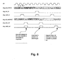
- the transaction propagates to each module 36 at a rate of one module per clock cycle.
- Fig. 6 depicts various bus signal sequences available on the bus lines 40 and 42. As seen, when an address is detected that belongs to the particular module 36, the request reg_ack_out signal is enabled and whenever such a signal as enabled is received by another module 36, the transaction is passed unhindered.
- a first transaction involves a request at an address (adreq) seen on the reg_ad_in lines, accompanied by a valid reg_valid_in signal. This is interpreted as a read to one of the registers 44 and the bus controller 60 responds with a response (resp) on the reg_ad_out lines and valid reg_ack_out and reg_valid_out signals. That output is then considered by the next module 36, where it is passed unhindered, but with a one-cycle delay.
- a rise time td_r of the bus is no more than two nanoseconds.
- a first and simplest method is to limit the bus to a single request/response at any one time. Although expensive with respect to interrogation, such provides inherently for unambiguous identification of the response.
- a second method is to count clock cycles amongst a series of pipelined requests. Since each bus controller 60 operates with a defined 1-cycle delay, the required response can be determined from the delay between the request and the response.' This provides for quick testing of any and all modules.
- a third alternative is for the module from which a request is made, to return an address or other identifier with the response data.
- a 38-bit bus provides a randomly accessible communication link between individual modules within the LSI graphics co-processor device whilst providing that there is no bottleneck of conductors at any one specific location around the periphery of the device to which external connections are made. This allows for integrated circuit designer to distribute individual modules across the surface of the chip to ensure optimal location relative to each other whilst affording optimal communication with outside devices.
- the decoding operation depicted in Fig. 5 may be at least partly performed by the node communication module.
- Fig. 7 shows such an arrangement 80 having a node module 82 forming the node of a daisy-chain loop formed by data lines 40,42 and modules 86, only some of which are seen.
- module addresses are partly decoded by the node module 82 and distributed via a single address bus 84 connecting to each module 86.
- Each module 86 contains a further decoder, corresponding in function to the decoder 66 of Fig. 5 .
- an arrangement 90 has a node module 92 which acts to fully perform the address decoding operation where modules 96 in a daisy-chain loop of data lines 40,42 are provided with a unique address signal derived from a decoded bus 94.
- a node module 92 acts to fully perform the address decoding operation where modules 96 in a daisy-chain loop of data lines 40,42 are provided with a unique address signal derived from a decoded bus 94.
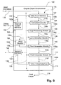
- Fig. 9 shows a graphic object co-processor 100 formed of a number of internal modules such as a video input interface 102, an instruction executor 104, an edge processing module 106, a level activation module 108, a pixel generation module 110, a pixel composite module 112, and a video output interface 114.
- Modules 102-114 form a pipeline 116 of processes by which the graphic object co-processor 100 processes an object description input 118 to form a pixel output 120.
- the pipeline 116 includes pipeline interconnections 116a-116f as illustrated interconnecting the various modules 102-114 in a pipeline fashion.
- Further modules such as a memory interface module 122 which couples to an external memory bus 124 and a JPEG decoder 126 are provided to facilitate the fetching or conversion of pixel-based object components and the like.
- pipeline segments 116a-116f convey rendering data and messages between the various modules 102-114, this being crucial to fast rendering of graphic object images
- a further bus 128 is provided within the co-processor 100 to allow for the interconnection of the various modules 102-126 in a fashion common to most integrated systems architectures.
- the video input interface 102 operates to couple the co-processor 100 to the object description input 118 to receive a page description language (PDL) representation of an image to be rendered including graphical objects and where appropriate organise such data into a form or order that can be manipulate by the pipeline 116.
- PDL page description language
- the object description input in a preferred configuration is supplied over a PCI bus, known in the art.
- the video input interface 102 also sorts command, control and instruction and object data that is not to be used early in the pipeline 116 from data to be immediately used providing for that other data to be temporarily stored in local memory coupled to the memory interface 122 via the bus 124.
- the instruction executor 104 reads and processes instructions from the received PDL and formats the instructions into messages that are transferred for interpretation and use by the remaining modules in the pipeline 116. Some instructions may be passed over the bus 128 and some via the pipeline segments 116b-116f, depending on their respective functions and whether it is necessary for the instruction to accompany data being processed (rendered) along the pipeline 116.
- the edge processing module 106 reads edge records derived from graphical objects described in the PDL, and determines a current scanline intersection for each edge in pixel position order across a rasterised display. This is preferably performed using a number of lists of active edges to enable sorting of the edge records into display order for each scanline.
- the edge processing module 106 outputs along the pipeline connection 116c to the level activation module 108.
- the level activation module 108 receives messages from the instruction executor 104 relating to priority level and fill data relating to graphical objects on the current scanline. Information contained in those message is preferably formed into a level activation table of graphical object properties.
- the edge crossing data received from the edge processing module 106 acts upon the table to determine those objects that are active for runs of pixels between adjacent edges and that contribute to the image being rendered. Such a process preferably takes account of objects having different opacity, as well as clipping objects.
- the pixel generation module 110 receives the active runs and determines for each object the pixel colour, or run of colour to be used for each pixel location between the active edges. This may include an opaque colour, a colour blend or a pixel-based image windowed by the corresponding graphical object. Where the latter is the case, the actual pixel data may be fetched via the memory interface 122 over the bus 128. Where the image is in a compressed form, the compressed data extracted onto the bus 128 is decompressed by the JPEG decoder 126 before being supplied to the pixel generation module 110.
- the pixel data for each contributing object is then forwarded to the pixel composite module 112 where the pixel values for all active objects at the current pixel location, or run of pixel locations, on the current scanline, are composited together according to their priority ordering to give and rendered pixel value for the location or run of locations.
- the video output interface 114 receives the rendered pixels via the connection 116f and performs a buffering interface role to ensure that the pixel output 120 is formed into an appropriate raster data sequence of pixel values for each scanline of the displayed image so rendered.
- the memory interface 122 provides for the use of memory external to the graphics co-processor 100 in the various processing stages along the pipeline 116.
- a pipeline module may be involve in complicated and time-consuming processing, such as the compositing function, other preceding modules may be stalled. In such circumstances, data messages and the like may be temporarily stored in the external memory until such time as the stalled process becomes available.
- the pixel composite module 112 uses stack machines to perform evaluate expression tree-based compositing expressions. Depending on the size of such expressions (ie. the number of contributing active objects) or the complexity of the object (eg. a pixel image), external memory may be used to build and evaluate the stack.
- an external control interface module 130 which couples to an external debug bus 132 which provides for the debugging of the operation of the co-processor 100.
- the debug bus 132 via the external control interface 130, couples to a debug loop bus 134 having segments 136a-136j which sequentially interconnect each of the various modules 102-126 with the external control interface in a manner corresponding to the functionality shown in Figs. 3-5 .
- the debug loop bus 134 thus provides for debugging of the operation of any of the modules 102-126 through access via the debug bus 132.
- the debug loop 134 and its segments 136a-136j are isolated from the processing pipeline 116, and its corresponding interconnecting segments 116a-116f, and also isolated from the main bus 128.
- the debugging of the operation of any one of the modules 102-126 may be performed without interrupting the render processing of the object description input 128 that provides the pixel output 120.
- the debug loop bus 134 gives access to registers and memories within the video input interface 102.
- the bus 134 is used to test those memories by writing and reading back test patterns.
- the bus 134 can be used to monitor activity in the video input interface 102. Such monitoring includes observing address pointers, job size counters, and data unpacking counters.
- PCI configuration registers containing PCI configuration settings associated with the input 118 are also observable on the bus 134 so that the state of the input 118 may be monitored.
- the bus 134 also forms a mechanism for enabling, checking and clearing interrupts from the video input interface 102, and generating software reset for the co-processor 100.
- Status registers within the instruction executor 104 accessible via the debug loop bus 134 show an address of a current instruction being fetched from the local memory connected to the memory interface 122 and bus 122 and the current instruction being decoded. Using the bus 134 is also possible to send abort a rendering job by writing to a configuration register within the instruction executor 104.
- Edge Processing module is accessible via the debug loop bus 134 to show the address of edges currently being fetched fr6m the local memory via the memory interface 122.
- Status registers in the level activation module 108 show the current x-coordinate and the current operation being processed by the level activation module 108.
- An output fill cache provided to buffer active object data from the level activation module 108 can also be turned off using a configuration register incorporated in the level activation module 108. All memories within the level activation module 108, such as the level activation table discussed above, are also available for interrogation via the debug loop bus 134 using read and write operations. If the level activation module 108 detects any priority levels out of order, or still active at the end of a line, they are also indicated in a status register accessible using the debug loop bus 134.
- Status registers in the pixel generation module 110 include current cache control signals and a composite bus output and are available for examination using the debug loop bus 134.
- a fill table within the pixel generation module 110 is also available on the debug loop bus 134 for read and write operation.
- Status registers accessible using the debug loop bus 134 within the pixel composite module 112 include a register identifying the particular compositing mode being used (either RGBO or CMYK), an attribute mode and a current composited colour and corresponding pipeline control signals.
- An un-premultiply division look-up table used for evaluating the compositing stack is also readable on the debug loop bus 134. In the case of overflow or underflow of the compositing stack, such is indicated in a dedicated status register.
- Registers in the video output interface 114 allow for the configuration of an output data format and transfer protocol.
- the co-processor 100 may be configured so that output pins supplying the pixel output 120 may be set to show output data to the debug loop bus 134.
- Status registers in the video output interface 114 are used to indicate desirable information such as the current x-coordinate, length of the scanline and the location and size of a memory dump buffer (if it exists), which may be used where the rendered image is to be stored rather that immediately displayed. If an illegal instruction has been detected, such can also be indicated in a register within the video output interface 114 also accessible using the debug loop bus 134.
- Status registers in the JPEG decoder 126 show if the decoder 126 is actively executing a decompression task, and if so, provide access to the parameters of the current task, such as the number of colour channels being processed, the type of operation, the type of transformation, the status of the list of tasks and the input data FIFO registers used in such a module. Also, low-level debug support information is provided to enable monitoring of data, such as current task address, current data fetch address, current data write address and data output, from various pipelined submodules arranged within the JPEG decoder 126. All memories formed within the JPEG decoder 126 are also available on the debug loop bus 134 for read and write operations.
- the memory interface 122 contains status registers which are useful for debugging and also used for manufacturing testing. Registers useful for debugging include the particular read address being accessed, along with an associated burst_size for burst memory transfers, read_address_valid, and read_address_taken. The latter two registers are useful to show the pattern of read requests and the visibility of the request/grant signals which can be representative of stalling patterns. Similarly, a write request status is also available. Details regarding current and previous ones of the modules 102 -126 granted access to the local memory via the memory interface 122 are also available in a common status register which give further information on the request patterns of modules relative to each other.
- the debug loop bus 134 allows those registers to be made visible as outputs for very little cost.
- the external control interface 130 can work in both master and slave modes. Since this part of the co-processor 100 is complicated, a bus adjacent to a clock domain boundary crossing is visible in debug mode, which makes debugging a simple task. Further, since control signals which arrive at the co-processor 100 at the external control interface 130 are simultaneously visible, it is possible to observe protocol violations using the debug loop bus 134 which may expose a fault that could otherwise be impossible to find.
- the external control interface 130 which is the master of the debug loop bus 134, repeats all read transactions every single clock cycle thereby allowing continuous monitoring. Repeat behaviour continues until either debug mode is turned off or a different transaction comes along, in which case the latter transaction becomes the one that is repeated.
Landscapes
- Engineering & Computer Science (AREA)
- Theoretical Computer Science (AREA)
- Physics & Mathematics (AREA)
- General Engineering & Computer Science (AREA)
- General Physics & Mathematics (AREA)
- Bus Control (AREA)
- Debugging And Monitoring (AREA)
- Tests Of Electronic Circuits (AREA)
Applications Claiming Priority (2)
| Application Number | Priority Date | Filing Date | Title |
|---|---|---|---|
| AUPQ0050A AUPQ005099A0 (en) | 1999-04-29 | 1999-04-29 | Sequential bus architecture |
| AUPQ005099 | 1999-04-29 |
Publications (3)
| Publication Number | Publication Date |
|---|---|
| EP1049021A2 EP1049021A2 (en) | 2000-11-02 |
| EP1049021A3 EP1049021A3 (en) | 2004-01-21 |
| EP1049021B1 true EP1049021B1 (en) | 2009-01-07 |
Family
ID=3814250
Family Applications (1)
| Application Number | Title | Priority Date | Filing Date |
|---|---|---|---|
| EP00303602A Expired - Lifetime EP1049021B1 (en) | 1999-04-29 | 2000-04-28 | Sequential bus architecture |
Country Status (5)
| Country | Link |
|---|---|
| US (1) | US6662256B1 (enExample) |
| EP (1) | EP1049021B1 (enExample) |
| JP (1) | JP4761487B2 (enExample) |
| AU (1) | AUPQ005099A0 (enExample) |
| DE (1) | DE60041300D1 (enExample) |
Cited By (2)
| Publication number | Priority date | Publication date | Assignee | Title |
|---|---|---|---|---|
| US7719892B2 (en) | 2005-09-30 | 2010-05-18 | Mosaid Technologies Incorproated | Flash memory device with data output control |
| US8654601B2 (en) | 2005-09-30 | 2014-02-18 | Mosaid Technologies Incorporated | Memory with output control |
Families Citing this family (16)
| Publication number | Priority date | Publication date | Assignee | Title |
|---|---|---|---|---|
| US6934785B2 (en) * | 2000-12-22 | 2005-08-23 | Micron Technology, Inc. | High speed interface with looped bus |
| US7032134B2 (en) * | 2001-03-28 | 2006-04-18 | Intel Corporation | Microprocessor design support for computer system and platform validation |
| US20030172190A1 (en) * | 2001-07-02 | 2003-09-11 | Globespanvirata Incorporated | Communications system using rings architecture |
| US20030195989A1 (en) * | 2001-07-02 | 2003-10-16 | Globespan Virata Incorporated | Communications system using rings architecture |
| JP4838458B2 (ja) * | 2001-09-13 | 2011-12-14 | 富士通セミコンダクター株式会社 | 半導体装置 |
| KR100477641B1 (ko) * | 2002-01-15 | 2005-03-23 | 삼성전자주식회사 | 버스 시스템 및 그 데이터 전송경로 결정방법 |
| US7113488B2 (en) * | 2002-04-24 | 2006-09-26 | International Business Machines Corporation | Reconfigurable circular bus |
| US7360007B2 (en) * | 2002-08-30 | 2008-04-15 | Intel Corporation | System including a segmentable, shared bus |
| US20070027485A1 (en) * | 2005-07-29 | 2007-02-01 | Kallmyer Todd A | Implantable medical device bus system and method |
| US20070076502A1 (en) * | 2005-09-30 | 2007-04-05 | Pyeon Hong B | Daisy chain cascading devices |
| US20080263248A1 (en) * | 2007-04-20 | 2008-10-23 | Harriman David J | Multi-drop extension for a communication protocol |
| US9035957B1 (en) * | 2007-08-15 | 2015-05-19 | Nvidia Corporation | Pipeline debug statistics system and method |
| EP2372490A1 (en) * | 2010-03-31 | 2011-10-05 | Robert Bosch GmbH | Circuit arrangement for a data processing system and method for data processing |
| DE102010003521A1 (de) * | 2010-03-31 | 2011-10-06 | Robert Bosch Gmbh | Modulare Struktur zur Datenverarbeitung |
| US11127110B2 (en) * | 2017-03-01 | 2021-09-21 | Arm Limited | Data processing systems |
| CN111522757B (zh) * | 2020-04-23 | 2023-08-22 | 上海琪云工业科技有限公司 | 一种基于i2c总线的中断读取与清除的控制方法 |
Family Cites Families (16)
| Publication number | Priority date | Publication date | Assignee | Title |
|---|---|---|---|---|
| US4378589A (en) * | 1976-12-27 | 1983-03-29 | International Business Machines Corporation | Undirectional looped bus microcomputer architecture |
| US4263736A (en) * | 1978-10-11 | 1981-04-28 | Colorado Time Systems, Inc. | Modular display system |
| US4356404A (en) * | 1981-05-26 | 1982-10-26 | Gte Automatic Electric Labs Inc. | Circuit for equipping a variable number of bus units on a closed loop bus |
| US4641308A (en) * | 1984-01-03 | 1987-02-03 | Texas Instruments Incorporated | Method of internal self-test of microprocessor using microcode |
| US4816993A (en) * | 1984-12-24 | 1989-03-28 | Hitachi, Ltd. | Parallel processing computer including interconnected operation units |
| DE3603751A1 (de) * | 1986-02-06 | 1987-08-13 | Siemens Ag | Informationsuebergabesystem zur uebergabe von binaeren informationen |
| FR2605768B1 (fr) * | 1986-10-23 | 1989-05-05 | Bull Sa | Dispositif de commande de bus constitue par plusieurs segments isolables |
| US4916647A (en) * | 1987-06-26 | 1990-04-10 | Daisy Systems Corporation | Hardwired pipeline processor for logic simulation |
| JPH0646413B2 (ja) * | 1987-08-10 | 1994-06-15 | 日本電気株式会社 | デ−タ処理プロセッサ |
| US5119481A (en) * | 1987-12-22 | 1992-06-02 | Kendall Square Research Corporation | Register bus multiprocessor system with shift |
| JPH01274539A (ja) * | 1988-04-27 | 1989-11-02 | Fujitsu Ltd | リングネットワーク |
| US5347515A (en) * | 1992-03-27 | 1994-09-13 | Pittway Corporation | Method and apparatus for global polling having contention-based address identification |
| US5375097A (en) * | 1993-06-29 | 1994-12-20 | Reddy; Chitranjan N. | Segmented bus architecture for improving speed in integrated circuit memories |
| GB9510509D0 (en) * | 1995-05-24 | 1995-07-19 | Thomson Consumer Electronics | A digital data bus system including arbitration |
| JPH0991262A (ja) * | 1995-09-20 | 1997-04-04 | Fuji Xerox Co Ltd | マルチプロセッサシステム |
| JP3202648B2 (ja) * | 1997-04-11 | 2001-08-27 | 甲府日本電気株式会社 | データ転送装置およびデータ転送システム |
-
1999
- 1999-04-29 AU AUPQ0050A patent/AUPQ005099A0/en not_active Abandoned
-
2000
- 2000-04-21 US US09/553,856 patent/US6662256B1/en not_active Expired - Lifetime
- 2000-04-28 EP EP00303602A patent/EP1049021B1/en not_active Expired - Lifetime
- 2000-04-28 DE DE60041300T patent/DE60041300D1/de not_active Expired - Lifetime
- 2000-04-28 JP JP2000131103A patent/JP4761487B2/ja not_active Expired - Fee Related
Cited By (5)
| Publication number | Priority date | Publication date | Assignee | Title |
|---|---|---|---|---|
| US7719892B2 (en) | 2005-09-30 | 2010-05-18 | Mosaid Technologies Incorproated | Flash memory device with data output control |
| US8000144B2 (en) | 2005-09-30 | 2011-08-16 | Mosaid Technologies Incorporated | Method and system for accessing a flash memory device |
| US8654601B2 (en) | 2005-09-30 | 2014-02-18 | Mosaid Technologies Incorporated | Memory with output control |
| US8743610B2 (en) | 2005-09-30 | 2014-06-03 | Conversant Intellectual Property Management Inc. | Method and system for accessing a flash memory device |
| US9230654B2 (en) | 2005-09-30 | 2016-01-05 | Conversant Intellectual Property Management Inc. | Method and system for accessing a flash memory device |
Also Published As
| Publication number | Publication date |
|---|---|
| JP4761487B2 (ja) | 2011-08-31 |
| EP1049021A3 (en) | 2004-01-21 |
| DE60041300D1 (de) | 2009-02-26 |
| JP2001005776A (ja) | 2001-01-12 |
| AUPQ005099A0 (en) | 1999-05-20 |
| EP1049021A2 (en) | 2000-11-02 |
| US6662256B1 (en) | 2003-12-09 |
Similar Documents
| Publication | Publication Date | Title |
|---|---|---|
| EP1049021B1 (en) | Sequential bus architecture | |
| US7328300B2 (en) | Method and system for keeping two independent busses coherent | |
| US5455915A (en) | Computer system with bridge circuitry having input/output multiplexers and third direct unidirectional path for data transfer between buses operating at different rates | |
| US4961140A (en) | Apparatus and method for extending a parallel synchronous data and message bus | |
| US6675248B1 (en) | Apparatus, method and system for accelerated graphics port bus bridges | |
| US7079146B2 (en) | Image producing device | |
| US6150679A (en) | FIFO architecture with built-in intelligence for use in a graphics memory system for reducing paging overhead | |
| US6766386B2 (en) | Method and interface for improved efficiency in performing bus-to-bus read data transfers | |
| US5129065A (en) | Apparatus and methods for interface register handshake for controlling devices | |
| CN100363912C (zh) | 集成电路、使用它的图像输入输出装置及其方法 | |
| JPH07191935A (ja) | データ処理システム及びデータ転送方法 | |
| EP0945810A2 (en) | Pipeline-type multi-processor system | |
| AU749664B2 (en) | Sequential bus architecture | |
| US20030110338A1 (en) | Method and apparatus for emulating computer buses using point-to-point techniues | |
| US6757762B1 (en) | Multi-mode processor bus bridge | |
| US5175832A (en) | Modular memory employing varying number of imput shift register stages | |
| US7916146B1 (en) | Halt context switching method and system | |
| JP3096405B2 (ja) | コンピュータシステム | |
| JP3216931B2 (ja) | バスサイジングを有するマイクロプロセッサ | |
| JPH0528856B2 (enExample) | ||
| US20060190660A1 (en) | Data ordering translation between linear and interleaved domains at a bus interface | |
| Miner | Miner | |
| CN101278277A (zh) | 运算处理装置 | |
| JPH05342172A (ja) | マルチプロセッサシステム | |
| EP1246068A2 (en) | System and method for monitoring data, computer program and data storage therefore |
Legal Events
| Date | Code | Title | Description |
|---|---|---|---|
| PUAI | Public reference made under article 153(3) epc to a published international application that has entered the european phase |
Free format text: ORIGINAL CODE: 0009012 |
|
| AK | Designated contracting states |
Kind code of ref document: A2 Designated state(s): AT BE CH CY DE DK ES FI FR GB GR IE IT LI LU MC NL PT SE |
|
| AX | Request for extension of the european patent |
Free format text: AL;LT;LV;MK;RO;SI |
|
| PUAL | Search report despatched |
Free format text: ORIGINAL CODE: 0009013 |
|
| AK | Designated contracting states |
Kind code of ref document: A3 Designated state(s): AT BE CH CY DE DK ES FI FR GB GR IE IT LI LU MC NL PT SE |
|
| AX | Request for extension of the european patent |
Extension state: AL LT LV MK RO SI |
|
| RIC1 | Information provided on ipc code assigned before grant |
Ipc: 7G 06F 13/42 A |
|
| 17P | Request for examination filed |
Effective date: 20040611 |
|
| AKX | Designation fees paid |
Designated state(s): DE FR GB IT |
|
| GRAP | Despatch of communication of intention to grant a patent |
Free format text: ORIGINAL CODE: EPIDOSNIGR1 |
|
| GRAS | Grant fee paid |
Free format text: ORIGINAL CODE: EPIDOSNIGR3 |
|
| GRAA | (expected) grant |
Free format text: ORIGINAL CODE: 0009210 |
|
| AK | Designated contracting states |
Kind code of ref document: B1 Designated state(s): DE FR GB IT |
|
| REG | Reference to a national code |
Ref country code: GB Ref legal event code: FG4D |
|
| REF | Corresponds to: |
Ref document number: 60041300 Country of ref document: DE Date of ref document: 20090226 Kind code of ref document: P |
|
| PLBE | No opposition filed within time limit |
Free format text: ORIGINAL CODE: 0009261 |
|
| STAA | Information on the status of an ep patent application or granted ep patent |
Free format text: STATUS: NO OPPOSITION FILED WITHIN TIME LIMIT |
|
| 26N | No opposition filed |
Effective date: 20091008 |
|
| REG | Reference to a national code |
Ref country code: FR Ref legal event code: PLFP Year of fee payment: 17 |
|
| REG | Reference to a national code |
Ref country code: FR Ref legal event code: PLFP Year of fee payment: 18 |
|
| PGFP | Annual fee paid to national office [announced via postgrant information from national office to epo] |
Ref country code: DE Payment date: 20170430 Year of fee payment: 18 Ref country code: FR Payment date: 20170425 Year of fee payment: 18 Ref country code: GB Payment date: 20170420 Year of fee payment: 18 |
|
| PGFP | Annual fee paid to national office [announced via postgrant information from national office to epo] |
Ref country code: IT Payment date: 20170421 Year of fee payment: 18 |
|
| REG | Reference to a national code |
Ref country code: DE Ref legal event code: R119 Ref document number: 60041300 Country of ref document: DE |
|
| GBPC | Gb: european patent ceased through non-payment of renewal fee |
Effective date: 20180428 |
|
| PG25 | Lapsed in a contracting state [announced via postgrant information from national office to epo] |
Ref country code: DE Free format text: LAPSE BECAUSE OF NON-PAYMENT OF DUE FEES Effective date: 20181101 |
|
| PG25 | Lapsed in a contracting state [announced via postgrant information from national office to epo] |
Ref country code: GB Free format text: LAPSE BECAUSE OF NON-PAYMENT OF DUE FEES Effective date: 20180428 |
|
| PG25 | Lapsed in a contracting state [announced via postgrant information from national office to epo] |
Ref country code: IT Free format text: LAPSE BECAUSE OF NON-PAYMENT OF DUE FEES Effective date: 20180428 Ref country code: FR Free format text: LAPSE BECAUSE OF NON-PAYMENT OF DUE FEES Effective date: 20180430 |