EP1048406A2 - Tête de support pour le polissage mécano-chimique d'un substrat - Google Patents
Tête de support pour le polissage mécano-chimique d'un substrat Download PDFInfo
- Publication number
- EP1048406A2 EP1048406A2 EP00303393A EP00303393A EP1048406A2 EP 1048406 A2 EP1048406 A2 EP 1048406A2 EP 00303393 A EP00303393 A EP 00303393A EP 00303393 A EP00303393 A EP 00303393A EP 1048406 A2 EP1048406 A2 EP 1048406A2
- Authority
- EP
- European Patent Office
- Prior art keywords
- substrate
- lip portion
- carrier head
- chamber
- flexible membrane
- Prior art date
- Legal status (The legal status is an assumption and is not a legal conclusion. Google has not performed a legal analysis and makes no representation as to the accuracy of the status listed.)
- Withdrawn
Links
- 239000000758 substrate Substances 0.000 title claims abstract description 151
- 238000005498 polishing Methods 0.000 title claims abstract description 103
- 239000000126 substance Substances 0.000 title claims abstract description 16
- 239000012528 membrane Substances 0.000 claims abstract description 72
- 238000000034 method Methods 0.000 claims description 28
- 239000012530 fluid Substances 0.000 claims description 15
- 238000004891 communication Methods 0.000 claims description 9
- 125000006850 spacer group Chemical group 0.000 claims description 8
- 230000002093 peripheral effect Effects 0.000 claims description 2
- 239000002002 slurry Substances 0.000 description 10
- KWYUFKZDYYNOTN-UHFFFAOYSA-M Potassium hydroxide Chemical compound [OH-].[K+] KWYUFKZDYYNOTN-UHFFFAOYSA-M 0.000 description 3
- 230000000694 effects Effects 0.000 description 3
- 239000002245 particle Substances 0.000 description 3
- 238000005096 rolling process Methods 0.000 description 3
- VYPSYNLAJGMNEJ-UHFFFAOYSA-N Silicium dioxide Chemical compound O=[Si]=O VYPSYNLAJGMNEJ-UHFFFAOYSA-N 0.000 description 2
- 239000000853 adhesive Substances 0.000 description 2
- 230000001070 adhesive effect Effects 0.000 description 2
- 239000003795 chemical substances by application Substances 0.000 description 2
- 238000007517 polishing process Methods 0.000 description 2
- 238000003825 pressing Methods 0.000 description 2
- 229920000181 Ethylene propylene rubber Polymers 0.000 description 1
- XUIMIQQOPSSXEZ-UHFFFAOYSA-N Silicon Chemical compound [Si] XUIMIQQOPSSXEZ-UHFFFAOYSA-N 0.000 description 1
- 230000002411 adverse Effects 0.000 description 1
- 239000012298 atmosphere Substances 0.000 description 1
- YACLQRRMGMJLJV-UHFFFAOYSA-N chloroprene Chemical compound ClC(=C)C=C YACLQRRMGMJLJV-UHFFFAOYSA-N 0.000 description 1
- 239000002131 composite material Substances 0.000 description 1
- 230000003750 conditioning effect Effects 0.000 description 1
- 230000003247 decreasing effect Effects 0.000 description 1
- 239000008367 deionised water Substances 0.000 description 1
- 229910021641 deionized water Inorganic materials 0.000 description 1
- 230000008021 deposition Effects 0.000 description 1
- 239000013013 elastic material Substances 0.000 description 1
- 229920001971 elastomer Polymers 0.000 description 1
- 239000004744 fabric Substances 0.000 description 1
- 239000011152 fibreglass Substances 0.000 description 1
- 230000002452 interceptive effect Effects 0.000 description 1
- 238000004519 manufacturing process Methods 0.000 description 1
- 239000000463 material Substances 0.000 description 1
- 239000004033 plastic Substances 0.000 description 1
- 229920003023 plastic Polymers 0.000 description 1
- 229920001084 poly(chloroprene) Polymers 0.000 description 1
- 229920001296 polysiloxane Polymers 0.000 description 1
- 238000007789 sealing Methods 0.000 description 1
- 229910052710 silicon Inorganic materials 0.000 description 1
- 239000010703 silicon Substances 0.000 description 1
- 239000000377 silicon dioxide Substances 0.000 description 1
- 235000012239 silicon dioxide Nutrition 0.000 description 1
- 239000007921 spray Substances 0.000 description 1
- 238000012876 topography Methods 0.000 description 1
- 235000012431 wafers Nutrition 0.000 description 1
- XLYOFNOQVPJJNP-UHFFFAOYSA-N water Chemical compound O XLYOFNOQVPJJNP-UHFFFAOYSA-N 0.000 description 1
Images


Classifications
-
- H—ELECTRICITY
- H01—ELECTRIC ELEMENTS
- H01L—SEMICONDUCTOR DEVICES NOT COVERED BY CLASS H10
- H01L21/00—Processes or apparatus adapted for the manufacture or treatment of semiconductor or solid state devices or of parts thereof
- H01L21/02—Manufacture or treatment of semiconductor devices or of parts thereof
- H01L21/04—Manufacture or treatment of semiconductor devices or of parts thereof the devices having potential barriers, e.g. a PN junction, depletion layer or carrier concentration layer
- H01L21/18—Manufacture or treatment of semiconductor devices or of parts thereof the devices having potential barriers, e.g. a PN junction, depletion layer or carrier concentration layer the devices having semiconductor bodies comprising elements of Group IV of the Periodic Table or AIIIBV compounds with or without impurities, e.g. doping materials
- H01L21/30—Treatment of semiconductor bodies using processes or apparatus not provided for in groups H01L21/20 - H01L21/26
- H01L21/302—Treatment of semiconductor bodies using processes or apparatus not provided for in groups H01L21/20 - H01L21/26 to change their surface-physical characteristics or shape, e.g. etching, polishing, cutting
-
- B—PERFORMING OPERATIONS; TRANSPORTING
- B24—GRINDING; POLISHING
- B24B—MACHINES, DEVICES, OR PROCESSES FOR GRINDING OR POLISHING; DRESSING OR CONDITIONING OF ABRADING SURFACES; FEEDING OF GRINDING, POLISHING, OR LAPPING AGENTS
- B24B37/00—Lapping machines or devices; Accessories
- B24B37/27—Work carriers
- B24B37/30—Work carriers for single side lapping of plane surfaces
Definitions
- Integrated circuits are typically formed on substrates, particularly silicon wafers, by the sequential deposition of conductive, semiconductive or insulative layers. After each layer is deposited, it is etched to create circuitry features. As a series of layers are sequentially deposited and etched, the outer or uppermost surface of the substrate, i.e., the exposed surface of the substrate, becomes increasingly nonplanar. This nonplanar surface presents problems in the photolithographic steps of the integrated circuit fabrication process. Therefore, there is a need to periodically planarize the substrate surface.
- the substrate is vacuum-chucked to the underside of the carrier head, and the carrier head is used to remove the substrate from the polishing pad.
- the carrier head is retracted from the polishing pad, the substrate is lifted off the pad.
- the substrate will remain on the polishing pad when the carrier head retracts. This may cause the substrate to fracture or chip.
- failure to remove the substrate can cause a machine fault requiring manual intervention. This requires shutting down the polishing apparatus, decreasing throughput. To achieve reliable operation from the polishing apparatus, the substrate removal process should be essentially flawless.
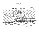
- FIG. 7D illustrates a method of removing the substrate from the carrier head using the carrier head of FIG. 6.
- FIG. 4A (for simplicity, only the elements involved in attaching and removing the substrate are illustrated in FIGS. 4A and 4B), when chamber 190 is evacuated, inner portion 180 of flexible membrane 118 is pulled inwardly. This causes a decrease in pressure in the volume between the backside of the substrate and the mounting surface of the flexible membrane. The decrease in pressure causes lip portion 186 to be drawn against a perimeter portion of the substrate to form a seal therebetween. This provides an effective vacuum-chuck of the substrate to the flexible membrane.
- the seal is sufficiently fluid-tight that it may not be necessary to apply an additional downward force to the portion of the flexible membrane over the perimeter of the substrate to form the seal. Consequently, the seal may be implemented without requiring additional pneumatic controls in the carrier head.
- juncture 184 to pivot downwardly. Consequently, lip portion 186 pivots upwardly so that it lifts away from the substrate. This breaks the seal between the flexible membrane and substrate, and the downward pressure from the inner portion of the flexible membrane removes the substrate from the carrier head.
- the thickness of juncture 184 should be selected to provide sufficient rigidity to ensure that the lip portion pivots upwardly when the inner portion of flexible membrane 118 is urged downwardly.
Landscapes
- Engineering & Computer Science (AREA)
- Mechanical Engineering (AREA)
- Physics & Mathematics (AREA)
- Condensed Matter Physics & Semiconductors (AREA)
- General Physics & Mathematics (AREA)
- Manufacturing & Machinery (AREA)
- Computer Hardware Design (AREA)
- Microelectronics & Electronic Packaging (AREA)
- Power Engineering (AREA)
- Finish Polishing, Edge Sharpening, And Grinding By Specific Grinding Devices (AREA)
- Mechanical Treatment Of Semiconductor (AREA)
Applications Claiming Priority (2)
| Application Number | Priority Date | Filing Date | Title |
|---|---|---|---|
| US09/296,935 US6210255B1 (en) | 1998-09-08 | 1999-04-22 | Carrier head for chemical mechanical polishing a substrate |
| US296935 | 1999-04-22 |
Publications (2)
| Publication Number | Publication Date |
|---|---|
| EP1048406A2 true EP1048406A2 (fr) | 2000-11-02 |
| EP1048406A3 EP1048406A3 (fr) | 2003-01-02 |
Family
ID=23144162
Family Applications (1)
| Application Number | Title | Priority Date | Filing Date |
|---|---|---|---|
| EP00303393A Withdrawn EP1048406A3 (fr) | 1999-04-22 | 2000-04-20 | Tête de support pour le polissage mécano-chimique d'un substrat |
Country Status (5)
| Country | Link |
|---|---|
| US (1) | US6210255B1 (fr) |
| EP (1) | EP1048406A3 (fr) |
| JP (1) | JP4516662B2 (fr) |
| KR (1) | KR20000071788A (fr) |
| SG (1) | SG96551A1 (fr) |
Cited By (3)
| Publication number | Priority date | Publication date | Assignee | Title |
|---|---|---|---|---|
| WO2002059947A2 (fr) * | 2001-01-11 | 2002-08-01 | Nutool, Inc. | Tete support pour retenir une plaquette et permettre le traitement d'une face avant de celle-ci |
| WO2003032374A2 (fr) * | 2001-10-11 | 2003-04-17 | Speedfam-Ipec Corporation | Porte-piece avec zones de pression et barrieres |
| DE102004058708B4 (de) * | 2003-12-05 | 2009-04-16 | Kabushiki Kaisha Toshiba | Polierkopf, Poliervorrichtung sowie Polierverfahren |
Families Citing this family (55)
| Publication number | Priority date | Publication date | Assignee | Title |
|---|---|---|---|---|
| DE10230707A1 (de) * | 2002-07-08 | 2004-01-22 | BSH Bosch und Siemens Hausgeräte GmbH | Kältegerät mit Türöffnungshilfe |
| US6146259A (en) * | 1996-11-08 | 2000-11-14 | Applied Materials, Inc. | Carrier head with local pressure control for a chemical mechanical polishing apparatus |
| US6183354B1 (en) | 1996-11-08 | 2001-02-06 | Applied Materials, Inc. | Carrier head with a flexible membrane for a chemical mechanical polishing system |
| US6165058A (en) * | 1998-12-09 | 2000-12-26 | Applied Materials, Inc. | Carrier head for chemical mechanical polishing |
| US6494774B1 (en) | 1999-07-09 | 2002-12-17 | Applied Materials, Inc. | Carrier head with pressure transfer mechanism |
| US6855043B1 (en) | 1999-07-09 | 2005-02-15 | Applied Materials, Inc. | Carrier head with a modified flexible membrane |
| US6358121B1 (en) | 1999-07-09 | 2002-03-19 | Applied Materials, Inc. | Carrier head with a flexible membrane and an edge load ring |
| JP3683149B2 (ja) * | 2000-02-01 | 2005-08-17 | 株式会社東京精密 | 研磨装置の研磨ヘッドの構造 |
| US6450868B1 (en) | 2000-03-27 | 2002-09-17 | Applied Materials, Inc. | Carrier head with multi-part flexible membrane |
| US7140956B1 (en) | 2000-03-31 | 2006-11-28 | Speedfam-Ipec Corporation | Work piece carrier with adjustable pressure zones and barriers and a method of planarizing a work piece |
| US6390905B1 (en) * | 2000-03-31 | 2002-05-21 | Speedfam-Ipec Corporation | Workpiece carrier with adjustable pressure zones and barriers |
| US6558232B1 (en) * | 2000-05-12 | 2003-05-06 | Multi-Planar Technologies, Inc. | System and method for CMP having multi-pressure zone loading for improved edge and annular zone material removal control |
| US6623343B2 (en) * | 2000-05-12 | 2003-09-23 | Multi Planar Technologies, Inc. | System and method for CMP head having multi-pressure annular zone subcarrier material removal control |
| US6722965B2 (en) * | 2000-07-11 | 2004-04-20 | Applied Materials Inc. | Carrier head with flexible membranes to provide controllable pressure and loading area |
| US20040005842A1 (en) * | 2000-07-25 | 2004-01-08 | Chen Hung Chih | Carrier head with flexible membrane |
| US6471571B2 (en) * | 2000-08-23 | 2002-10-29 | Rodel Holdings, Inc. | Substrate supporting carrier pad |
| US6508696B1 (en) * | 2000-08-25 | 2003-01-21 | Mitsubishi Materials Corporation | Wafer-polishing head and polishing apparatus having the same |
| JP2002187060A (ja) * | 2000-10-11 | 2002-07-02 | Ebara Corp | 基板保持装置、ポリッシング装置、及び研磨方法 |
| US6641461B2 (en) * | 2001-03-28 | 2003-11-04 | Multi Planar Technologyies, Inc. | Chemical mechanical polishing apparatus having edge, center and annular zone control of material removal |
| KR100437089B1 (ko) * | 2001-05-23 | 2004-06-23 | 삼성전자주식회사 | 화학기계적 연마장치의 연마헤드 |
| KR100470227B1 (ko) * | 2001-06-07 | 2005-02-05 | 두산디앤디 주식회사 | 화학기계적 연마장치의 캐리어 헤드 |
| US6712673B2 (en) | 2001-10-04 | 2004-03-30 | Memc Electronic Materials, Inc. | Polishing apparatus, polishing head and method |
| EP1453081A4 (fr) * | 2001-12-06 | 2008-07-09 | Ebara Corp | Dispositif de support de substrat et dispositif de polissage |
| US6841057B2 (en) * | 2002-03-13 | 2005-01-11 | Applied Materials Inc. | Method and apparatus for substrate polishing |
| JP4353673B2 (ja) | 2002-04-18 | 2009-10-28 | 株式会社荏原製作所 | ポリッシング方法 |
| KR100481872B1 (ko) * | 2003-01-14 | 2005-04-11 | 삼성전자주식회사 | 폴리싱 헤드 및 화학적 기계적 연마 장치 |
| TWI323017B (en) * | 2003-02-10 | 2010-04-01 | Ebara Corp | Substrate holding apparatus and polishing apparatus |
| US7001245B2 (en) * | 2003-03-07 | 2006-02-21 | Applied Materials Inc. | Substrate carrier with a textured membrane |
| US20050181711A1 (en) * | 2004-02-12 | 2005-08-18 | Alexander Starikov | Substrate confinement apparatus and method |
| KR100621629B1 (ko) * | 2004-06-04 | 2006-09-19 | 삼성전자주식회사 | 화학적 기계적 연마 장치에 사용되는 연마 헤드 및 연마방법 |
| JP4822744B2 (ja) * | 2004-06-04 | 2011-11-24 | 三星電子株式会社 | 化学機械的研磨装置、キャリアヘッド及び区画リング |
| EP1807865B1 (fr) * | 2004-11-01 | 2012-04-11 | Ebara Corporation | Appareil de polissage |
| KR100674923B1 (ko) * | 2004-12-03 | 2007-01-26 | 삼성전자주식회사 | 인접한 화소간에 출력회로를 공유하는 씨모스 이미지 센서 |
| JP5112614B2 (ja) * | 2004-12-10 | 2013-01-09 | 株式会社荏原製作所 | 基板保持装置および研磨装置 |
| JP4814677B2 (ja) * | 2006-03-31 | 2011-11-16 | 株式会社荏原製作所 | 基板保持装置および研磨装置 |
| JP5009101B2 (ja) * | 2006-10-06 | 2012-08-22 | 株式会社荏原製作所 | 基板研磨装置 |
| US7727055B2 (en) * | 2006-11-22 | 2010-06-01 | Applied Materials, Inc. | Flexible membrane for carrier head |
| US7651384B2 (en) * | 2007-01-09 | 2010-01-26 | Applied Materials, Inc. | Method and system for point of use recycling of ECMP fluids |
| US7731572B2 (en) * | 2007-05-24 | 2010-06-08 | United Microelectronics Corp. | CMP head |
| WO2009066351A1 (fr) * | 2007-11-20 | 2009-05-28 | Shin-Etsu Handotai Co., Ltd. | Tête de polissage et appareil de polissage |
| US7959496B2 (en) * | 2008-01-03 | 2011-06-14 | Strasbaugh | Flexible membrane assembly for a CMP system and method of using |
| KR101722540B1 (ko) * | 2008-03-25 | 2017-04-03 | 어플라이드 머티어리얼스, 인코포레이티드 | 캐리어 헤드 멤브레인 |
| DE112009002112B4 (de) * | 2008-08-29 | 2023-01-05 | Shin-Etsu Handotai Co., Ltd. | Polierkopf und Poliervorrichtung |
| US8475231B2 (en) * | 2008-12-12 | 2013-07-02 | Applied Materials, Inc. | Carrier head membrane |
| US10160093B2 (en) | 2008-12-12 | 2018-12-25 | Applied Materials, Inc. | Carrier head membrane roughness to control polishing rate |
| JP5648954B2 (ja) * | 2010-08-31 | 2015-01-07 | 不二越機械工業株式会社 | 研磨装置 |
| KR101196652B1 (ko) * | 2011-05-31 | 2012-11-02 | 주식회사 케이씨텍 | 캐리어 헤드의 멤브레인 결합체 및 이를 구비한 캐리어 헤드 |
| US10319982B2 (en) | 2013-02-01 | 2019-06-11 | Encell Technology, Inc. | Coated iron electrode and method of making same |
| KR102332801B1 (ko) * | 2015-05-06 | 2021-11-30 | 주식회사 케이씨텍 | 기판 연마장치의 디척 방법 |
| US10669023B2 (en) | 2016-02-19 | 2020-06-02 | Raytheon Company | Tactical aerial platform |
| US11267099B2 (en) | 2017-09-27 | 2022-03-08 | Taiwan Semiconductor Manufacturing Company, Ltd. | Chemical mechanical planarization membrane |
| CN111936267B (zh) | 2018-03-13 | 2023-07-25 | 应用材料公司 | 化学机械研磨机中的耗材部件监控 |
| SG10202008012WA (en) * | 2019-08-29 | 2021-03-30 | Ebara Corp | Elastic membrane and substrate holding apparatus |
| US11728203B2 (en) * | 2020-10-13 | 2023-08-15 | Canon Kabushiki Kaisha | Chuck assembly, planarization process, apparatus and method of manufacturing an article |
| CN114918721B (zh) * | 2022-06-27 | 2023-12-05 | 江苏常北宸机械有限公司 | 一种汽车减震内管及外管生产用倒角装置及倒角方法 |
Citations (3)
| Publication number | Priority date | Publication date | Assignee | Title |
|---|---|---|---|---|
| US5624299A (en) * | 1993-12-27 | 1997-04-29 | Applied Materials, Inc. | Chemical mechanical polishing apparatus with improved carrier and method of use |
| EP0859399A2 (fr) * | 1997-02-13 | 1998-08-19 | Integrated Process Equipment Corp. | Appareil de polissage de tranche de semiconducteur avec plaque de support flexible |
| EP0879678A1 (fr) * | 1997-05-23 | 1998-11-25 | Applied Materials, Inc. | Plaque de support avec dispositif de détection de substrat pour un dispositif de polissage mécano-chimique |
Family Cites Families (22)
| Publication number | Priority date | Publication date | Assignee | Title |
|---|---|---|---|---|
| DE3313707C2 (de) | 1983-04-15 | 1985-02-07 | B. Bacher GmbH, 7204 Wurmlingen | Kopierrahmen |
| US4669915A (en) | 1985-11-19 | 1987-06-02 | Shell Offshore Inc. | Manipulator apparatus with flexible membrane for gripping submerged objects |
| US4918869A (en) | 1987-10-28 | 1990-04-24 | Fujikoshi Machinery Corporation | Method for lapping a wafer material and an apparatus therefor |
| JP2527232B2 (ja) | 1989-03-16 | 1996-08-21 | 株式会社日立製作所 | 研磨装置 |
| US5193316A (en) | 1991-10-29 | 1993-03-16 | Texas Instruments Incorporated | Semiconductor wafer polishing using a hydrostatic medium |
| US5205082A (en) | 1991-12-20 | 1993-04-27 | Cybeq Systems, Inc. | Wafer polisher head having floating retainer ring |
| US5643053A (en) | 1993-12-27 | 1997-07-01 | Applied Materials, Inc. | Chemical mechanical polishing apparatus with improved polishing control |
| US5423716A (en) | 1994-01-05 | 1995-06-13 | Strasbaugh; Alan | Wafer-handling apparatus having a resilient membrane which holds wafer when a vacuum is applied |
| US5449316A (en) | 1994-01-05 | 1995-09-12 | Strasbaugh; Alan | Wafer carrier for film planarization |
| JP3158934B2 (ja) | 1995-02-28 | 2001-04-23 | 三菱マテリアル株式会社 | ウェーハ研磨装置 |
| US5908530A (en) | 1995-05-18 | 1999-06-01 | Obsidian, Inc. | Apparatus for chemical mechanical polishing |
| US5643061A (en) | 1995-07-20 | 1997-07-01 | Integrated Process Equipment Corporation | Pneumatic polishing head for CMP apparatus |
| ATE228915T1 (de) | 1996-01-24 | 2002-12-15 | Lam Res Corp | Halbleiterscheiben-polierkopf |
| JP3663767B2 (ja) | 1996-09-04 | 2005-06-22 | 信越半導体株式会社 | 薄板の鏡面研磨装置 |
| US6183354B1 (en) | 1996-11-08 | 2001-02-06 | Applied Materials, Inc. | Carrier head with a flexible membrane for a chemical mechanical polishing system |
| US6146259A (en) | 1996-11-08 | 2000-11-14 | Applied Materials, Inc. | Carrier head with local pressure control for a chemical mechanical polishing apparatus |
| US6056632A (en) | 1997-02-13 | 2000-05-02 | Speedfam-Ipec Corp. | Semiconductor wafer polishing apparatus with a variable polishing force wafer carrier head |
| US5870793A (en) * | 1997-05-02 | 1999-02-16 | Integrated Process Equipment Corp. | Brush for scrubbing semiconductor wafers |
| DE19728962A1 (de) * | 1997-06-30 | 1999-01-07 | Siemens Ag | Vorrichtung zum Ätzen einer Halbleiterscheibe |
| US5964653A (en) | 1997-07-11 | 1999-10-12 | Applied Materials, Inc. | Carrier head with a flexible membrane for a chemical mechanical polishing system |
| US5993302A (en) | 1997-12-31 | 1999-11-30 | Applied Materials, Inc. | Carrier head with a removable retaining ring for a chemical mechanical polishing apparatus |
| US6124146A (en) * | 1998-05-15 | 2000-09-26 | Motorola, Inc. | Resistless device fabrication method |
-
1999
- 1999-04-22 US US09/296,935 patent/US6210255B1/en not_active Expired - Lifetime
-
2000
- 2000-04-20 EP EP00303393A patent/EP1048406A3/fr not_active Withdrawn
- 2000-04-22 KR KR1020000021464A patent/KR20000071788A/ko not_active Application Discontinuation
- 2000-04-22 SG SG200002270A patent/SG96551A1/en unknown
- 2000-04-24 JP JP2000122904A patent/JP4516662B2/ja not_active Expired - Lifetime
Patent Citations (3)
| Publication number | Priority date | Publication date | Assignee | Title |
|---|---|---|---|---|
| US5624299A (en) * | 1993-12-27 | 1997-04-29 | Applied Materials, Inc. | Chemical mechanical polishing apparatus with improved carrier and method of use |
| EP0859399A2 (fr) * | 1997-02-13 | 1998-08-19 | Integrated Process Equipment Corp. | Appareil de polissage de tranche de semiconducteur avec plaque de support flexible |
| EP0879678A1 (fr) * | 1997-05-23 | 1998-11-25 | Applied Materials, Inc. | Plaque de support avec dispositif de détection de substrat pour un dispositif de polissage mécano-chimique |
Cited By (7)
| Publication number | Priority date | Publication date | Assignee | Title |
|---|---|---|---|---|
| WO2002059947A2 (fr) * | 2001-01-11 | 2002-08-01 | Nutool, Inc. | Tete support pour retenir une plaquette et permettre le traitement d'une face avant de celle-ci |
| WO2002059947A3 (fr) * | 2001-01-11 | 2003-03-20 | Nutool Inc | Tete support pour retenir une plaquette et permettre le traitement d'une face avant de celle-ci |
| US6716084B2 (en) | 2001-01-11 | 2004-04-06 | Nutool, Inc. | Carrier head for holding a wafer and allowing processing on a front face thereof to occur |
| WO2003032374A2 (fr) * | 2001-10-11 | 2003-04-17 | Speedfam-Ipec Corporation | Porte-piece avec zones de pression et barrieres |
| WO2003032374A3 (fr) * | 2001-10-11 | 2004-02-05 | Speedfam Ipec Corp | Porte-piece avec zones de pression et barrieres |
| US6746318B2 (en) | 2001-10-11 | 2004-06-08 | Speedfam-Ipec Corporation | Workpiece carrier with adjustable pressure zones and barriers |
| DE102004058708B4 (de) * | 2003-12-05 | 2009-04-16 | Kabushiki Kaisha Toshiba | Polierkopf, Poliervorrichtung sowie Polierverfahren |
Also Published As
| Publication number | Publication date |
|---|---|
| EP1048406A3 (fr) | 2003-01-02 |
| KR20000071788A (ko) | 2000-11-25 |
| US6210255B1 (en) | 2001-04-03 |
| JP4516662B2 (ja) | 2010-08-04 |
| SG96551A1 (en) | 2003-06-16 |
| JP2000354960A (ja) | 2000-12-26 |
Similar Documents
| Publication | Publication Date | Title |
|---|---|---|
| US6210255B1 (en) | Carrier head for chemical mechanical polishing a substrate | |
| US6159079A (en) | Carrier head for chemical mechanical polishing a substrate | |
| US6645044B2 (en) | Method of chemical mechanical polishing with controllable pressure and loading area | |
| US6277009B1 (en) | Carrier head including a flexible membrane and a compliant backing member for a chemical mechanical polishing apparatus | |
| US6277014B1 (en) | Carrier head with a flexible membrane for chemical mechanical polishing | |
| US6165058A (en) | Carrier head for chemical mechanical polishing | |
| EP1754571B1 (fr) | Bague de maintien pour un dispositif de polissage mécano-chimique | |
| EP1001864B1 (fr) | Tete de polissage comportant une commande de pression localisee pour dispositif de polissage chimiomecanique | |
| US6241593B1 (en) | Carrier head with pressurizable bladder | |
| US6776694B2 (en) | Methods for carrier head with multi-part flexible membrane | |
| EP1048408A2 (fr) | Tête support comprenant une membrane compressible | |
| US6358121B1 (en) | Carrier head with a flexible membrane and an edge load ring | |
| US20030079836A1 (en) | Carrier head for chemical mechanical polishing | |
| JP4519972B2 (ja) | 化学機械研磨の制御可能圧力及びローディング領域を有するキャリヤヘッド |
Legal Events
| Date | Code | Title | Description |
|---|---|---|---|
| PUAI | Public reference made under article 153(3) epc to a published international application that has entered the european phase |
Free format text: ORIGINAL CODE: 0009012 |
|
| AK | Designated contracting states |
Kind code of ref document: A2 Designated state(s): AT BE CH CY DE DK ES FI FR GB GR IE IT LI LU MC NL PT SE |
|
| AX | Request for extension of the european patent |
Free format text: AL;LT;LV;MK;RO;SI |
|
| PUAL | Search report despatched |
Free format text: ORIGINAL CODE: 0009013 |
|
| AK | Designated contracting states |
Kind code of ref document: A3 Designated state(s): AT BE CH CY DE DK ES FI FR GB GR IE IT LI LU MC NL PT SE |
|
| AX | Request for extension of the european patent |
Free format text: AL;LT;LV;MK;RO;SI |
|
| AKX | Designation fees paid | ||
| REG | Reference to a national code |
Ref country code: DE Ref legal event code: 8566 |
|
| STAA | Information on the status of an ep patent application or granted ep patent |
Free format text: STATUS: THE APPLICATION IS DEEMED TO BE WITHDRAWN |
|
| 18D | Application deemed to be withdrawn |
Effective date: 20030703 |