EP1047148A2 - Nichtreziproke Schaltungsanordnung und Kommunikationsgerät - Google Patents
Nichtreziproke Schaltungsanordnung und Kommunikationsgerät Download PDFInfo
- Publication number
- EP1047148A2 EP1047148A2 EP00108475A EP00108475A EP1047148A2 EP 1047148 A2 EP1047148 A2 EP 1047148A2 EP 00108475 A EP00108475 A EP 00108475A EP 00108475 A EP00108475 A EP 00108475A EP 1047148 A2 EP1047148 A2 EP 1047148A2
- Authority
- EP
- European Patent Office
- Prior art keywords
- ferrite
- major surface
- ground plate
- matching
- degrees
- Prior art date
- Legal status (The legal status is an assumption and is not a legal conclusion. Google has not performed a legal analysis and makes no representation as to the accuracy of the status listed.)
- Granted
Links
Images


Classifications
-
- H—ELECTRICITY
- H01—ELECTRIC ELEMENTS
- H01P—WAVEGUIDES; RESONATORS, LINES, OR OTHER DEVICES OF THE WAVEGUIDE TYPE
- H01P1/00—Auxiliary devices
- H01P1/32—Non-reciprocal transmission devices
- H01P1/38—Circulators
- H01P1/383—Junction circulators, e.g. Y-circulators
- H01P1/387—Strip line circulators
-
- H—ELECTRICITY
- H01—ELECTRIC ELEMENTS
- H01P—WAVEGUIDES; RESONATORS, LINES, OR OTHER DEVICES OF THE WAVEGUIDE TYPE
- H01P1/00—Auxiliary devices
- H01P1/32—Non-reciprocal transmission devices
- H01P1/36—Isolators
-
- H—ELECTRICITY
- H01—ELECTRIC ELEMENTS
- H01P—WAVEGUIDES; RESONATORS, LINES, OR OTHER DEVICES OF THE WAVEGUIDE TYPE
- H01P1/00—Auxiliary devices
- H01P1/32—Non-reciprocal transmission devices
- H01P1/38—Circulators
- H01P1/383—Junction circulators, e.g. Y-circulators
-
- H—ELECTRICITY
- H01—ELECTRIC ELEMENTS
- H01P—WAVEGUIDES; RESONATORS, LINES, OR OTHER DEVICES OF THE WAVEGUIDE TYPE
- H01P1/00—Auxiliary devices
- H01P1/32—Non-reciprocal transmission devices
- H01P1/38—Circulators
- H01P1/393—Circulators using Faraday rotators
Definitions
- the present invention relates to a nonreciprocal circuit device. More particularly, the present invention relates to a nonreciprocal circuit device such as an isolator or a circulator for use in a microwave communication apparatus, and to a communication apparatus using the isolator or circulator.
- a nonreciprocal circuit device such as an isolator or a circulator for use in a microwave communication apparatus, and to a communication apparatus using the isolator or circulator.
- the function of a lumped-constant type isolator is to pass a signal only in a transmitting direction and to eliminate the transmission of the signal in the reverse direction.
- the lumped-constant type isolator 11 comprises a terminal case 13 which is made of resin and disposed on a lower yoke 12.
- the lower yoke 12 is made of magnetic metal and comprises right and left side walls 12a and a bottom wall 12b.
- a center electrode assembly 14 is accommodated in the terminal case 13 and an upper yoke 15 made of magnetic metal is placed thereon. Inside the upper yoke 15, a permanent magnet 16 is disposed. The permanent magnet 16 applies a DC magnetic field to the center electrode assembly 14.
- the center electrode assembly 14 comprises a microwave ferrite 20 and three center electrodes 21, 22 and 23 disposed on the microwave ferrite 20.
- the three center electrodes 21-23 cross each other at angles of 120 degrees in an electrically insulated state.
- Port sections P1, P2 and P3 at first ends of the three center electrodes 21-23 are bent vertically and a shield section 26 which is common to the other ends of the three center electrodes 21-23 is contacted to the lower surface of the ferrite 20.
- the common shield section 26 substantially covers the lower surface of the ferrite 20, and is connected to the bottom wall 12b of the lower yoke 12 through a window 13a of the terminal case 13.
- Input/Output electrodes 31, 32 and ground terminals 33, 34 are insert molded in the terminal case 13. First ends of the Input/Output electrodes 31, 32 are exposed outside the side wall of the case 13, and the other ends thereof are exposed inside the side wall of the case 13, to thereby form Input/Output connecting sections 18a, 18b inside the case 13. Similarly, first ends of the ground terminals 33, 34 are exposed outside the side wall of the case 13, and the other ends thereof are exposed inside the side wall of the case 13, to thereby form ground connecting electrode sections 17a, 17b and 17c, 17d, respectively.
- Each of the port sections P1-P3 of the center electrodes 21-23 is connected to a hot-side capacitor electrode 1 of one of matching capacitors C1, C2 and C3.
- a cold-side capacitor electrode 2 of each of the matching capacitors C1-C3 is connected to the ground connecting electrode sections 17a, 17b, 17c, 17d.
- One end of a termination resistor R is connected to the hot-side capacitor electrode 1 of the matching capacitor C3, and the other end thereof is connected to the ground connecting electrode section 17b. That is, the matching capacitor C3 and the termination resistor R are electrically connected in parallel between the port section P3 of the center electrode 23 and ground.
- the port sections P1 and P2 are connected to the Input/Output connecting electrode sections 18a and 18b, respectively.
- each of the matching capacitors C1-C3 must be inserted between one of the port sections P1-P3 and one of the ground connecting electrode sections 17a, 17c, 17d, respectively, while holding the capacitor in a vertical orientation. Further, it is necessary to connect the capacitor electrodes 1, 2 of the matching capacitors C1-C3 to the port sections P1-P3 and the ground connecting electrode sections 17a, 17c, 17d by soldering.
- the isolator 11 has the problem that the process of inserting the matching capacitors C1-C3 between the port sections P1-P3 and the ground connecting electrode sections 17a, 17c, 17d requires much time and effort, because the matching capacitors C1-C3 are small in size and difficult to handle.
- the port sections P1-P3 of the center electrodes 21-23 must be bent vertically in one of the initial steps in the assembly process, it is possible for the solder connection between the port sections P1-P3 and the matching capacitors C1-C3 to become unstable because of variations in the bend angle of the port sections P1-P3.
- the solder it is possible for the solder to spill and cause a short-circuit between the hot-side capacitor electrodes 1 and the cold-side capacitor electrodes 2 of the matching capacitors C1-C3, resulting in a defective product.
- preferred embodiments of the present invention provide a nonreciprocal circuit device and a communication apparatus having high reliability, including a matching capacitor which is easy to assemble.
- One embodiment of the present invention provides a nonreciprocal circuit device, comprising: a permanent magnet; a ferrite to which a DC magnetic field is applied by the permanent magnet; a plurality of center electrodes extending from a first major surface of the ferrite to a second major surface of the ferrite via side surfaces of the ferrite; a ground plate disposed on the second major surface side of the ferrite and electrically connected to the plurality of center electrodes; a plurality of matching capacitors electrically connected between the ground plate and port sections of the plurality of center electrodes respectively; and at least one matching capacitor being disposed such that a major surface thereof forms an angle in a range of 60 degrees to 120 degrees with a major surface of the ferrite.
- the matching capacitors can be connected between the center electrodes and the ground plate assembled with the ferrite in an initial assembly step.
- an insulator for preventing a short circuit may be provided in the vicinity of the portion of the ground plate at which the matching capacitor is connected and in the vicinity of the port section of the center electrode. This insulator prevents an undesirable solder bridge from being formed by spilled solder when the matching capacitor is soldered. By this, for example, a short-circuit between the hot-side capacitor electrode and the cold-side capacitor electrode of the matching capacitor can be prevented.
- a communication apparatus has a lower manufacturing cost and higher reliability because the apparatus is provided with a nonreciprocal circuit device having the above described arrangement.
- Fig. 1 shows an exploded perspective view of a first embodiment of a nonreciprocal circuit device of the present invention.
- the nonreciprocal circuit device 41 is one which the present invention is applied to the lumped-constant type isolator 11 explained by referring to Fig. 10.
- the lumped-constant type isolator 41 comprises a lower yoke 12, a terminal case 53 made of resin, a center electrode assembly 54, a permanent magnet 16 and an upper yoke.
- the lower yoke 12 is made of magnetic metal and comprises right and left side walls 12a and 12b.
- the terminal case 53 is disposed on the lower yoke 12, the center electrode assembly 54 is accommodated in the terminal case 13 and an upper yoke 15 made of magnetic metal is placed thereon.
- the permanent magnet 16 applies a DC magnetic field to the center electrode assembly 54.
- a magnetic circuit is formed by the lower yoke 12, the center electrode assembly 54 and the upper yoke 15.
- the center electrode assembly 54 comprises a microwave ferrite 20 and three center electrodes 21-23 disposed on the upper surface (first major surface) of the microwave ferrite 20, as shown in Fig. 2 and Fig. 3.
- the three center electrodes 21 23 cross each other at angles of 120 degrees in an electrically insulated state.
- Port sections P1-P3 at first ends of the three center electrodes 21-23 are bent vertically and a shield section 26 which is common to the other ends of the three center electrodes 21-23 is contacted to the lower surface (second major surface) of the ferrite 20.
- the common shield section 26 substantially covers the lower surface of the ferrite 20.
- a ground plate 42 is disposed on the lower surface side of the ferrite 20 and electrically connected to the common shield section of the center electrodes 21-23 by face-contact (by utilizing solder, electroconductive adhesive, etc. if necessary).
- Capacitor connecting sections 42a, 42b, 42c are extended from the end portion of the ground plate 42 and stand so as to be parallel to the port sections P1-P3 of the center electrodes 21-23.
- the ground plate 42 is grounded by connecting it to the bottom wall 12b of the lower yoke 12 through the window 53a of the terminal case 43.
- Hot-side capacitor electrodes 1 of matching capacitors C1-C3 are connected to the port sections P1-P3 by soldering, and cold-side capacitor electrodes 2 thereof are connected to the capacitor connecting sections 42a, 42b, 42c of the ground plate 42 by soldering.
- the matching capacitors C1-C3 are disposed such that the surfaces of the capacitor electrodes 1, 2 and the upper surface of the ferrite 20 form an angle in a range from 60 degrees to 120 degrees. In the case of this first embodiment, the angle is set at 90 degrees.
- Each of the matching capacitors C1-C3 is a single-plate type capacitor in which capacitor electrodes 1, 2 are formed on both surfaces of a dielectric substrate 3.
- the matching capacitors C1-C3 can be performed as indicated in Fig. 4, for example. That is, bend portions 43 are provided at the base portion of the ground plate 42 so that the device shown in Fig. 4 can be shaped as shown in Fig. 2. After applying soldering paste to the capacitor connecting sections 42a-42c of the ground plate 42, the matching capacitors C1-C3 are mounted such that the cold-side capacitor electrodes 2 are at the underside.
- the ferrite 20 including the attached center electrodes 21-23 is mounted from above.
- the common shield section 20 of the center electrodes 21-23 is face-contacted to the upper surface of the ground plate 42, and the port sections P1-P3 are face-contacted to the hot-side capacitor electrodes 1 of the matching capacitors C1-C3, respectively.
- the solder paste is heated in this state, and the matching capacitors C1-C3 are soldered.
- the capacitor connecting sections 42a-42c and the port sections P1-P3 are bent so as to dispose the matching capacitors C1-C3 with the surfaces of the capacitor electrodes 1, 2 and the upper surface of the ferrite 20 forming an angle in a range of 60 degrees to 120 degrees. Accordingly, the center electrode assembly 54 is obtained.
- Input/Output electrodes 31, 32 and ground terminals 33, 34 are insert molded in the terminal case 53. First ends of the Input/Output electrodes 31, 32 are exposed outside the side wall of the case 53, and the other ends thereof are exposed inside the side wall of the case 53, to form Input/Output connecting sections 18a, 18b. Similarly, a first end of the ground terminal 33 is exposed outside the side wall of the case 53, and the other end thereof is exposed inside the side wall of the case 53, to form ground connecting electrode section 17b.
- the center electrode assembly 54 and the termination resistor R are accommodated in the terminal case 53 having a structure as described above.
- the port sections P1, P2 of the center electrodes 21, 22 are connected to the Input/Output connecting electrode sections 18a, 18b by soldering, etc.
- One end of the termination resistor R is connected to the ground connecting electrode section 17b, and the other end thereof is connected to the hot-side capacitor electrode 1 of the matching capacitor C3.
- the equivalent circuit diagram of the isolator 41 is shown in Fig. 6.
- the matching capacitors C1-C3 are mounted between the port sections P1-P3 of the center electrodes 21-23 and the capacitor connecting sections 42a-42c of the ground plate 42 respectively, the matching capacitors C1-C3, the center electrodes 21-23 and the ferrite 20 can be handled as one unit. According to this arrangement, the process in which the small-sized matching capacitors C1-C3, which are difficult to handle, are mounted in a vertical plane, is eliminated, and thereby the manufacture of the isolator 41 becomes easier.
- the matching capacitors C1-C3 after connecting the matching capacitors C1-C3 to the port sections P1-P3 and the capacitor connecting sections 42a-42c, the matching capacitors C1-C3 are disposed vertically by bending the port sections P1 P3 and the capacitor connecting sections 42a-42c. Accordingly, compared with the conventional isolator 11 (see Fig. 10) in which the port section must be bent before connecting the matching capacitor, the soldering of the port sections P1 P3 and the matching capacitors C1-C3 can be performed with reliability, and thereby the connection reliability is improved.
- each of the cold-side electrodes 2 of the matching capacitors C1-C3 is grounded via the ground plate 42, the ground connecting electrode sections 17a, 17b, 17c formed in the conventional terminal case 13 (see Fig. 10) can be omitted. Accordingly, the structure of the terminal case 53 becomes simple and cost-reduction can be realized.
- a center electrode assembly 64 according to another embodiment of the nonreciprocal circuit device of the present invention is shown in Fig. 7 and Fig. 8
- insulators 65, 66 are provided for preventing solder bridges.
- the insulator 65 is provided on the ground plate 42 in the vicinity of where the matching capacitors C1-C3 are connected.
- the insulator 66 is provided in the vicinity of the port sections P1-P3 of the center electrodes 21-23.
- the insulators 65, 66 prevent a solder bridge and thereby prevent a short-circuit between the hot-side electrodes 1 of the matching capacitors C1-C3 and the ground electrode 42 or a short-circuit between the hot-side electrodes 1 and the cold-side electrodes 2. Further, since a solder bridge is eliminated by the insulators 65, 66, the positioning accuracy of the matching capacitors is improved.
- an insulator 67 is provided where the center electrodes 21, 22 and the hot-side electrodes 1 oppose each other.
- a third embodiment of the invention will be explained, taking a mobile phone as an example of a communication apparatus of the present invention.
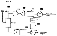
- Fig. 9 is a block diagram of an RF part of a circuit in a mobile phone 120.
- 122 denotes an antenna element
- 123 denotes a duplexer
- 131 denotes a transmission-side isolator
- 132 denotes a transmission-side amplifier
- 133 denotes a transmission-side band-pass filter
- 134 denotes a transmission-side mixer
- 135 denotes a reception-side amplifier
- 136 denotes a reception-side inter-stage band-pass filter
- 137 denotes a reception-side mixer
- 138 denotes a voltage control oscillator (VCO)
- VCO voltage control oscillator
- 139 denotes a local band-pass filter.
- the lumped-constant type isolator of the first and second embodiments can be used as the transmission-side isolator 131. By attaching this isolator, a mobile phone with low-cost and high-reliability cane be realized.
- the mounting of all of the matching capacitors C1-C3 is longitudinal, i.e., the capacitor electrode surfaces thereof are perpendicular to the horizontal surface.
- Two of the matching capacitors C1-C2 may be mounted longitudinally and the other one of the matching capacitors C3 may be mounted horizontally, in which the capacitor electrode surface thereof is parallel to the horizontal surface. That is, the advantages of the invention, such as saving space, reducing costs, and facilitating assembly, are obtained as long as at least one of the matching capacitors is disposed with the capacitor electrode face thereof forming an angle with the ferrite in a range of 60 degrees to 120 degrees.
- the mounting of the matching capacitors C1-C3 can be performed by electroconductive adhesive instead of by soldering.
- the matching capacitors C1-C3 may be monolithic-type capacitors.
- the present invention is also applicable to a nonreciprocal circuit device other than an isolator for use in other high-frequency components such as a circulator.
- the matching capacitors are mounted between center electrodes attached to a ferrite and a ground plate, the matching capacitors can be treated as one unit with the center electrodes, the ground plate and the ferrite. Accordingly, mounting of the small-sized matching capacitors, which are difficult to handle, becomes easier. The matching efficiency of the nonreciprocal circuit device is drastically improved, and thereby costs can be reduced. As a result, cost-reduction of a communication apparatus can be realized.
Landscapes
- Non-Reversible Transmitting Devices (AREA)
Applications Claiming Priority (4)
| Application Number | Priority Date | Filing Date | Title |
|---|---|---|---|
| JP11725499 | 1999-04-23 | ||
| JP11725499 | 1999-04-23 | ||
| JP2000038459 | 2000-02-16 | ||
| JP2000038459A JP2001007607A (ja) | 1999-04-23 | 2000-02-16 | 非可逆回路素子及び通信機装置 |
Publications (3)
| Publication Number | Publication Date |
|---|---|
| EP1047148A2 true EP1047148A2 (de) | 2000-10-25 |
| EP1047148A3 EP1047148A3 (de) | 2002-04-03 |
| EP1047148B1 EP1047148B1 (de) | 2003-07-16 |
Family
ID=26455397
Family Applications (1)
| Application Number | Title | Priority Date | Filing Date |
|---|---|---|---|
| EP00108475A Expired - Lifetime EP1047148B1 (de) | 1999-04-23 | 2000-04-18 | Nichtreziproke Schaltungsanordnung und Kommunikationsgerät |
Country Status (6)
| Country | Link |
|---|---|
| US (1) | US6633204B1 (de) |
| EP (1) | EP1047148B1 (de) |
| JP (1) | JP2001007607A (de) |
| KR (1) | KR100340452B1 (de) |
| CN (1) | CN1182622C (de) |
| DE (1) | DE60003868T2 (de) |
Families Citing this family (2)
| Publication number | Priority date | Publication date | Assignee | Title |
|---|---|---|---|---|
| JP2002368553A (ja) * | 2001-06-08 | 2002-12-20 | Mitsubishi Electric Corp | 高周波増幅器およびそれを用いた無線送信装置 |
| CN113381150B (zh) * | 2021-08-12 | 2021-10-29 | 中国电子科技集团公司第九研究所 | 基于电容并联的隔离器用塑封外壳及隔离器 |
Family Cites Families (7)
| Publication number | Priority date | Publication date | Assignee | Title |
|---|---|---|---|---|
| US4101850A (en) * | 1977-04-18 | 1978-07-18 | Motorola, Inc. | Uhf isolator using stacked conductor sheets |
| TW306106B (en) * | 1996-04-03 | 1997-05-21 | Deltec New Zealand | Circulator and its components |
| JPH10303605A (ja) * | 1997-04-25 | 1998-11-13 | Hitachi Metals Ltd | アイソレータ |
| JP3483191B2 (ja) * | 1997-07-31 | 2004-01-06 | 日立金属株式会社 | 非可逆回路素子 |
| JPH1168411A (ja) | 1997-08-08 | 1999-03-09 | Murata Mfg Co Ltd | 非可逆回路素子 |
| JP3307293B2 (ja) | 1997-09-17 | 2002-07-24 | 株式会社村田製作所 | 非可逆回路素子 |
| DE69821423D1 (de) * | 1997-09-17 | 2004-03-11 | Murata Manufacturing Co | Nichtreziproke Schaltungsanordnung |
-
2000
- 2000-02-16 JP JP2000038459A patent/JP2001007607A/ja active Pending
- 2000-04-18 EP EP00108475A patent/EP1047148B1/de not_active Expired - Lifetime
- 2000-04-18 DE DE60003868T patent/DE60003868T2/de not_active Expired - Lifetime
- 2000-04-22 KR KR1020000021429A patent/KR100340452B1/ko not_active Expired - Lifetime
- 2000-04-24 CN CNB001070533A patent/CN1182622C/zh not_active Expired - Lifetime
- 2000-04-24 US US09/557,456 patent/US6633204B1/en not_active Expired - Lifetime
Also Published As
| Publication number | Publication date |
|---|---|
| US6633204B1 (en) | 2003-10-14 |
| EP1047148B1 (de) | 2003-07-16 |
| KR100340452B1 (ko) | 2002-06-12 |
| CN1271974A (zh) | 2000-11-01 |
| DE60003868T2 (de) | 2004-05-19 |
| DE60003868D1 (de) | 2003-08-21 |
| JP2001007607A (ja) | 2001-01-12 |
| CN1182622C (zh) | 2004-12-29 |
| EP1047148A3 (de) | 2002-04-03 |
| KR20000071785A (ko) | 2000-11-25 |
Similar Documents
| Publication | Publication Date | Title |
|---|---|---|
| US6366178B1 (en) | Non-reciprocal circuit device with capacitor terminals integral with the ground plate | |
| EP1047148B1 (de) | Nichtreziproke Schaltungsanordnung und Kommunikationsgerät | |
| JP3680682B2 (ja) | 非可逆回路素子および通信機装置 | |
| JP3419369B2 (ja) | 非可逆回路素子 | |
| US6724276B2 (en) | Non-reciprocal circuit device and communication apparatus | |
| JP3705275B2 (ja) | 非可逆回路素子の製造方法及び通信機装置 | |
| JP3175303B2 (ja) | 非可逆回路素子 | |
| US20030067365A1 (en) | Nonreciprocal circuit element and communication device | |
| JP2606474Y2 (ja) | 非可逆回路素子 | |
| JP2606475Y2 (ja) | 非可逆回路素子 | |
| JP2553138Y2 (ja) | 誘電体フィルタ | |
| JPH01117502A (ja) | 非可逆回路素子 | |
| JP2003060410A (ja) | 非可逆回路素子及び通信装置 | |
| JPH08148908A (ja) | 非可逆回路素子 | |
| JPH03252202A (ja) | 非可逆回路素子 | |
| JPH1079606A (ja) | 非可逆回路素子 | |
| JPH03124103A (ja) | 非可逆回路素子 | |
| JP2002175906A (ja) | 抵抗素子及びそれを用いた非可逆回路素子及び通信装置 | |
| JP2000332510A (ja) | 非可逆回路素子 | |
| JPH0593105U (ja) | 非可逆回路素子 | |
| JP2002217610A (ja) | 非可逆回路素子及び通信装置 | |
| JPH0681102U (ja) | 誘電体フィルタ | |
| JP2000091811A (ja) | フィルタ装置 | |
| JP2002135006A (ja) | 非可逆回路素子及び通信装置 |
Legal Events
| Date | Code | Title | Description |
|---|---|---|---|
| PUAI | Public reference made under article 153(3) epc to a published international application that has entered the european phase |
Free format text: ORIGINAL CODE: 0009012 |
|
| 17P | Request for examination filed |
Effective date: 20000418 |
|
| AK | Designated contracting states |
Kind code of ref document: A2 Designated state(s): DE FR GB Kind code of ref document: A2 Designated state(s): AT BE CH CY DE DK ES FI FR GB GR IE IT LI LU MC NL PT SE |
|
| AX | Request for extension of the european patent |
Free format text: AL;LT;LV;MK;RO;SI |
|
| PUAL | Search report despatched |
Free format text: ORIGINAL CODE: 0009013 |
|
| AK | Designated contracting states |
Kind code of ref document: A3 Designated state(s): AT BE CH CY DE DK ES FI FR GB GR IE IT LI LU MC NL PT SE |
|
| AX | Request for extension of the european patent |
Free format text: AL;LT;LV;MK;RO;SI |
|
| AKX | Designation fees paid |
Free format text: DE FR GB |
|
| GRAH | Despatch of communication of intention to grant a patent |
Free format text: ORIGINAL CODE: EPIDOS IGRA |
|
| GRAH | Despatch of communication of intention to grant a patent |
Free format text: ORIGINAL CODE: EPIDOS IGRA |
|
| GRAA | (expected) grant |
Free format text: ORIGINAL CODE: 0009210 |
|
| AK | Designated contracting states |
Designated state(s): DE FR GB |
|
| PG25 | Lapsed in a contracting state [announced via postgrant information from national office to epo] |
Ref country code: FR Free format text: LAPSE BECAUSE OF FAILURE TO SUBMIT A TRANSLATION OF THE DESCRIPTION OR TO PAY THE FEE WITHIN THE PRESCRIBED TIME-LIMIT Effective date: 20030716 |
|
| REG | Reference to a national code |
Ref country code: GB Ref legal event code: FG4D |
|
| REG | Reference to a national code |
Ref country code: IE Ref legal event code: FG4D |
|
| REF | Corresponds to: |
Ref document number: 60003868 Country of ref document: DE Date of ref document: 20030821 Kind code of ref document: P |
|
| PLBE | No opposition filed within time limit |
Free format text: ORIGINAL CODE: 0009261 |
|
| STAA | Information on the status of an ep patent application or granted ep patent |
Free format text: STATUS: NO OPPOSITION FILED WITHIN TIME LIMIT |
|
| 26N | No opposition filed |
Effective date: 20040419 |
|
| EN | Fr: translation not filed | ||
| REG | Reference to a national code |
Ref country code: IE Ref legal event code: MM4A |
|
| PGFP | Annual fee paid to national office [announced via postgrant information from national office to epo] |
Ref country code: DE Payment date: 20190418 Year of fee payment: 20 |
|
| PGFP | Annual fee paid to national office [announced via postgrant information from national office to epo] |
Ref country code: GB Payment date: 20190418 Year of fee payment: 20 |
|
| REG | Reference to a national code |
Ref country code: DE Ref legal event code: R071 Ref document number: 60003868 Country of ref document: DE |
|
| REG | Reference to a national code |
Ref country code: GB Ref legal event code: PE20 Expiry date: 20200417 |
|
| PG25 | Lapsed in a contracting state [announced via postgrant information from national office to epo] |
Ref country code: GB Free format text: LAPSE BECAUSE OF EXPIRATION OF PROTECTION Effective date: 20200417 |