EP1045420B1 - Process for the manufacture of a plasma panel - Google Patents
Process for the manufacture of a plasma panel Download PDFInfo
- Publication number
- EP1045420B1 EP1045420B1 EP00400494A EP00400494A EP1045420B1 EP 1045420 B1 EP1045420 B1 EP 1045420B1 EP 00400494 A EP00400494 A EP 00400494A EP 00400494 A EP00400494 A EP 00400494A EP 1045420 B1 EP1045420 B1 EP 1045420B1
- Authority
- EP
- European Patent Office
- Prior art keywords
- barriers
- process according
- paste
- tile
- layer
- Prior art date
- Legal status (The legal status is an assumption and is not a legal conclusion. Google has not performed a legal analysis and makes no representation as to the accuracy of the status listed.)
- Expired - Lifetime
Links
Images
Classifications
-
- B—PERFORMING OPERATIONS; TRANSPORTING
- B65—CONVEYING; PACKING; STORING; HANDLING THIN OR FILAMENTARY MATERIAL
- B65D—CONTAINERS FOR STORAGE OR TRANSPORT OF ARTICLES OR MATERIALS, e.g. BAGS, BARRELS, BOTTLES, BOXES, CANS, CARTONS, CRATES, DRUMS, JARS, TANKS, HOPPERS, FORWARDING CONTAINERS; ACCESSORIES, CLOSURES, OR FITTINGS THEREFOR; PACKAGING ELEMENTS; PACKAGES
- B65D83/00—Containers or packages with special means for dispensing contents
- B65D83/0005—Containers or packages provided with a piston or with a movable bottom or partition having approximately the same section as the container
- B65D83/0033—Containers or packages provided with a piston or with a movable bottom or partition having approximately the same section as the container the piston being a follower-piston and the dispensing means comprising a hand-operated pressure-device at the opposite part of the container
-
- H—ELECTRICITY
- H01—ELECTRIC ELEMENTS
- H01J—ELECTRIC DISCHARGE TUBES OR DISCHARGE LAMPS
- H01J9/00—Apparatus or processes specially adapted for the manufacture, installation, removal, maintenance of electric discharge tubes, discharge lamps, or parts thereof; Recovery of material from discharge tubes or lamps
- H01J9/24—Manufacture or joining of vessels, leading-in conductors or bases
- H01J9/241—Manufacture or joining of vessels, leading-in conductors or bases the vessel being for a flat panel display
- H01J9/242—Spacers between faceplate and backplate
-
- H—ELECTRICITY
- H01—ELECTRIC ELEMENTS
- H01J—ELECTRIC DISCHARGE TUBES OR DISCHARGE LAMPS
- H01J9/00—Apparatus or processes specially adapted for the manufacture, installation, removal, maintenance of electric discharge tubes, discharge lamps, or parts thereof; Recovery of material from discharge tubes or lamps
- H01J9/24—Manufacture or joining of vessels, leading-in conductors or bases
- H01J9/245—Manufacture or joining of vessels, leading-in conductors or bases specially adapted for gas discharge tubes or lamps
-
- H—ELECTRICITY
- H01—ELECTRIC ELEMENTS
- H01J—ELECTRIC DISCHARGE TUBES OR DISCHARGE LAMPS
- H01J2211/00—Plasma display panels with alternate current induction of the discharge, e.g. AC-PDPs
- H01J2211/20—Constructional details
- H01J2211/34—Vessels, containers or parts thereof, e.g. substrates
- H01J2211/36—Spacers, barriers, ribs, partitions or the like
Definitions
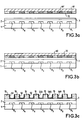
- the filler consists of an oxide such as alumina or silica. It may include a hardening agent in an amount equal to or less than 10% of the mass of the mineral filler.
- This hardening agent is chosen from a glassy phase, such as lead borosilicate or bismuth borosilicate or from a compound such as lead sulphate, lead phosphate, zinc phosphate, sodium silicate, potassium silicate or lead silicate, these being capable of forming chemical bonds at the treatment temperature.
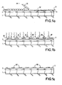
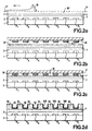
- the paste 30' is deposited uniformly over the layer 3 through the screen-printing mask 21, which has an aperture corresponding to the aspect ratio of the working surface of the tile.
- the paste has dried, it has a thickness of about 30 ⁇ m, the thickness being defined by the volume of the barriers to be formed.
Landscapes
- Engineering & Computer Science (AREA)
- Manufacturing & Machinery (AREA)
- Mechanical Engineering (AREA)
- Gas-Filled Discharge Tubes (AREA)
- Laminated Bodies (AREA)
Priority Applications (1)
| Application Number | Priority Date | Filing Date | Title |
|---|---|---|---|
| EP06119280A EP1753007A3 (en) | 1999-04-15 | 2000-02-23 | Process for the manufacture of a plasma panel |
Applications Claiming Priority (2)
| Application Number | Priority Date | Filing Date | Title |
|---|---|---|---|
| FR9904704 | 1999-04-15 | ||
| FR9904704A FR2792454B1 (fr) | 1999-04-15 | 1999-04-15 | Procede de fabrication d'un panneau a plasma |
Related Child Applications (1)
| Application Number | Title | Priority Date | Filing Date |
|---|---|---|---|
| EP06119280A Division EP1753007A3 (en) | 1999-04-15 | 2000-02-23 | Process for the manufacture of a plasma panel |
Publications (2)
| Publication Number | Publication Date |
|---|---|
| EP1045420A1 EP1045420A1 (en) | 2000-10-18 |
| EP1045420B1 true EP1045420B1 (en) | 2007-05-02 |
Family
ID=9544417
Family Applications (2)
| Application Number | Title | Priority Date | Filing Date |
|---|---|---|---|
| EP06119280A Withdrawn EP1753007A3 (en) | 1999-04-15 | 2000-02-23 | Process for the manufacture of a plasma panel |
| EP00400494A Expired - Lifetime EP1045420B1 (en) | 1999-04-15 | 2000-02-23 | Process for the manufacture of a plasma panel |
Family Applications Before (1)
| Application Number | Title | Priority Date | Filing Date |
|---|---|---|---|
| EP06119280A Withdrawn EP1753007A3 (en) | 1999-04-15 | 2000-02-23 | Process for the manufacture of a plasma panel |
Country Status (8)
| Country | Link |
|---|---|
| US (1) | US6527606B1 (xx) |
| EP (2) | EP1753007A3 (xx) |
| JP (1) | JP4693204B2 (xx) |
| KR (1) | KR100787619B1 (xx) |
| CN (1) | CN100349195C (xx) |
| DE (1) | DE60034624T2 (xx) |
| FR (1) | FR2792454B1 (xx) |
| TW (1) | TW475193B (xx) |
Families Citing this family (10)
| Publication number | Priority date | Publication date | Assignee | Title |
|---|---|---|---|---|
| US6544090B1 (en) * | 2000-06-16 | 2003-04-08 | E. I. Du Pont De Nemours And Company | Method for forming barrier structures on a substrate and the resulting article |
| KR100400370B1 (ko) * | 2001-04-02 | 2003-10-08 | 엘지전자 주식회사 | 플라즈마 디스플레이 패널의 제조방법 |
| US7176492B2 (en) * | 2001-10-09 | 2007-02-13 | 3M Innovative Properties Company | Method for forming ceramic microstructures on a substrate using a mold and articles formed by the method |
| US7033534B2 (en) * | 2001-10-09 | 2006-04-25 | 3M Innovative Properties Company | Method for forming microstructures on a substrate using a mold |
| FR2855644A1 (fr) * | 2003-05-27 | 2004-12-03 | Thomson Plasma | Panneau a plasma dont les barrieres de partionnement sont en ciment |
| JP4288475B2 (ja) * | 2003-06-12 | 2009-07-01 | セイコーエプソン株式会社 | ディスプレイ装置の製造方法と製造装置 |
| KR100612382B1 (ko) | 2003-11-29 | 2006-08-16 | 삼성에스디아이 주식회사 | 플라즈마 디스플레이 패널 및 그 제조 방법 |
| US20060043634A1 (en) * | 2004-08-26 | 2006-03-02 | 3M Innovative Properties Company | Method of forming microstructures with a discrete mold provided on a roller |
| WO2006104513A2 (en) * | 2004-08-26 | 2006-10-05 | 3M Innovative Properties Company | Method of forming microstructures with multiple discrete molds |
| JP2008511124A (ja) * | 2004-08-26 | 2008-04-10 | スリーエム イノベイティブ プロパティズ カンパニー | テンプレートで微細構造を形成する方法 |
Family Cites Families (15)
| Publication number | Priority date | Publication date | Assignee | Title |
|---|---|---|---|---|
| JPS5511262B2 (xx) * | 1974-05-21 | 1980-03-24 | ||
| JPH04109536A (ja) * | 1990-08-29 | 1992-04-10 | Mitsubishi Electric Corp | プラズマデイスプレイの製造方法 |
| JP2967617B2 (ja) * | 1991-08-06 | 1999-10-25 | 日本電気株式会社 | プラズマディスプレイパネルの製造方法 |
| JPH0745200A (ja) * | 1993-07-29 | 1995-02-14 | Noritake Co Ltd | プラズマディスプレイパネル |
| JP3684603B2 (ja) * | 1995-01-26 | 2005-08-17 | 松下電器産業株式会社 | プラズマディスプレイパネルの製造方法 |
| JP3472413B2 (ja) | 1996-06-28 | 2003-12-02 | 京セラ株式会社 | プラズマ表示装置用基板とこれを用いたプラズマ表示装置 |
| US5853446A (en) * | 1996-04-16 | 1998-12-29 | Corning Incorporated | Method for forming glass rib structures |
| JPH10188793A (ja) * | 1996-10-21 | 1998-07-21 | Hitachi Ltd | ガス放電型表示パネル、ガス放電型表示パネルの製造方法およびガス放電型表示パネルを用いた表示装置 |
| KR19980040884A (ko) * | 1996-11-30 | 1998-08-17 | 엄길용 | 플라즈마 표시소자의 격벽형성방법 |
| JP3690443B2 (ja) * | 1997-05-20 | 2005-08-31 | 大日本印刷株式会社 | プラズマディスプレイパネル |
| DE69826359T2 (de) * | 1997-04-30 | 2005-09-29 | Kyocera Corp. | Hertellungsverfahren eines Substrats für eine Plasma-Anzeigeeinheit |
| JP2958298B2 (ja) * | 1997-05-22 | 1999-10-06 | 三星電管株式會社 | プラズマ表示素子の隔壁製造方法及びその製造装置 |
| JPH10340668A (ja) * | 1997-06-04 | 1998-12-22 | Fujitsu Ltd | 表示パネルの隔壁形成装置 |
| JP3909725B2 (ja) * | 1997-08-05 | 2007-04-25 | 株式会社タイカ | ディスプレイパネル用基板の製造方法 |
| US6247986B1 (en) * | 1998-12-23 | 2001-06-19 | 3M Innovative Properties Company | Method for precise molding and alignment of structures on a substrate using a stretchable mold |
-
1999
- 1999-04-15 FR FR9904704A patent/FR2792454B1/fr not_active Expired - Fee Related
-
2000
- 2000-02-23 EP EP06119280A patent/EP1753007A3/en not_active Withdrawn
- 2000-02-23 DE DE60034624T patent/DE60034624T2/de not_active Expired - Lifetime
- 2000-02-23 EP EP00400494A patent/EP1045420B1/en not_active Expired - Lifetime
- 2000-03-17 TW TW089104883A patent/TW475193B/zh not_active IP Right Cessation
- 2000-03-29 CN CNB001055100A patent/CN100349195C/zh not_active Expired - Fee Related
- 2000-04-03 KR KR1020000017383A patent/KR100787619B1/ko not_active IP Right Cessation
- 2000-04-12 JP JP2000110836A patent/JP4693204B2/ja not_active Expired - Fee Related
- 2000-04-13 US US09/550,275 patent/US6527606B1/en not_active Expired - Fee Related
Non-Patent Citations (1)
| Title |
|---|
| None * |
Also Published As
| Publication number | Publication date |
|---|---|
| KR100787619B1 (ko) | 2007-12-21 |
| DE60034624D1 (de) | 2007-06-14 |
| CN1271154A (zh) | 2000-10-25 |
| FR2792454A1 (fr) | 2000-10-20 |
| EP1753007A3 (en) | 2008-02-13 |
| DE60034624T2 (de) | 2008-01-03 |
| US6527606B1 (en) | 2003-03-04 |
| CN100349195C (zh) | 2007-11-14 |
| JP2000323028A (ja) | 2000-11-24 |
| EP1045420A1 (en) | 2000-10-18 |
| EP1753007A2 (en) | 2007-02-14 |
| KR20000071549A (ko) | 2000-11-25 |
| FR2792454B1 (fr) | 2001-05-25 |
| TW475193B (en) | 2002-02-01 |
| JP4693204B2 (ja) | 2011-06-01 |
Similar Documents
| Publication | Publication Date | Title |
|---|---|---|
| EP1045420B1 (en) | Process for the manufacture of a plasma panel | |
| US6483238B1 (en) | Plasma display panel having a porous structure | |
| JP2000057941A (ja) | 表示パネルの組立てに用いる基板構体の製造方法及びシート状転写材料 | |
| US7339318B2 (en) | Plate for a plasma panel with reinforced porous barriers | |
| JP3860673B2 (ja) | プラズマディスプレイパネルおよびその製造方法 | |
| CN100362614C (zh) | 一种制作气体放电显示屏的方法 | |
| JP2814557B2 (ja) | ガス放電パネルの製造方法 | |
| KR20000037809A (ko) | 플라즈마 표시장치용 하부기판 및 그 제조방법 | |
| WO2003075301A1 (fr) | Ecran a plasma | |
| US7131880B2 (en) | Process for manufacturing barriers for a plasma display panel | |
| JP3379329B2 (ja) | プラズマディスプレイパネル用背面基板の製造方法 | |
| EP1085555A1 (en) | Composition for black matrix, formation of black matrix and display device provided with black matrix | |
| KR100267553B1 (ko) | 플라즈마 디스플레이 패널용 하부패널 제조방법 | |
| KR100444514B1 (ko) | 플라즈마 디스플레이 패널의 하판 및 그의 제조방법 | |
| JP3536554B2 (ja) | フラットディスプレイパネルの隔壁形成方法 | |
| JPH11283506A (ja) | プラズマ表示装置用基板及びその製造方法 | |
| KR100433220B1 (ko) | 플라즈마 디스플레이 패널의 하판 제조방법 | |
| KR100360884B1 (ko) | 플라즈마 디스플레이 패널 소자 및 그의 격벽 블랙층 제조방법 | |
| JP2000208042A (ja) | プラズマディスプレイパネルの隔壁形成方法 | |
| KR100696634B1 (ko) | 가스 방전 표시 장치 및 그 제조 방법 | |
| KR100582199B1 (ko) | 플라즈마 디스플레이 패널의 하판 및 그의 제조방법 | |
| JPH11135026A (ja) | プラズマディスプレイパネル | |
| JPH1167089A (ja) | 蛍光体層付隔壁の形成方法 | |
| JPH1167102A (ja) | プラズマディスプレイパネル及びその製造方法 | |
| KR20020071609A (ko) | 플라즈마 디스플레이 패널 소자의 상판 구조 및 그 제조방법 |
Legal Events
| Date | Code | Title | Description |
|---|---|---|---|
| PUAI | Public reference made under article 153(3) epc to a published international application that has entered the european phase |
Free format text: ORIGINAL CODE: 0009012 |
|
| AK | Designated contracting states |
Kind code of ref document: A1 Designated state(s): DE FR GB |
|
| AX | Request for extension of the european patent |
Free format text: AL;LT;LV;MK;RO;SI |
|
| 17P | Request for examination filed |
Effective date: 20010223 |
|
| AKX | Designation fees paid |
Free format text: DE FR GB |
|
| 17Q | First examination report despatched |
Effective date: 20030916 |
|
| GRAP | Despatch of communication of intention to grant a patent |
Free format text: ORIGINAL CODE: EPIDOSNIGR1 |
|
| RIN1 | Information on inventor provided before grant (corrected) |
Inventor name: BARET, GUY Inventor name: JOBERT, PIERRE-PAUL |
|
| GRAS | Grant fee paid |
Free format text: ORIGINAL CODE: EPIDOSNIGR3 |
|
| GRAA | (expected) grant |
Free format text: ORIGINAL CODE: 0009210 |
|
| AK | Designated contracting states |
Kind code of ref document: B1 Designated state(s): DE FR GB |
|
| REG | Reference to a national code |
Ref country code: GB Ref legal event code: FG4D |
|
| REF | Corresponds to: |
Ref document number: 60034624 Country of ref document: DE Date of ref document: 20070614 Kind code of ref document: P |
|
| ET | Fr: translation filed | ||
| PLBE | No opposition filed within time limit |
Free format text: ORIGINAL CODE: 0009261 |
|
| STAA | Information on the status of an ep patent application or granted ep patent |
Free format text: STATUS: NO OPPOSITION FILED WITHIN TIME LIMIT |
|
| 26N | No opposition filed |
Effective date: 20080205 |
|
| PGFP | Annual fee paid to national office [announced via postgrant information from national office to epo] |
Ref country code: DE Payment date: 20130219 Year of fee payment: 14 Ref country code: GB Payment date: 20130221 Year of fee payment: 14 Ref country code: FR Payment date: 20130301 Year of fee payment: 14 |
|
| REG | Reference to a national code |
Ref country code: DE Ref legal event code: R119 Ref document number: 60034624 Country of ref document: DE |
|
| GBPC | Gb: european patent ceased through non-payment of renewal fee |
Effective date: 20140223 |
|
| REG | Reference to a national code |
Ref country code: FR Ref legal event code: ST Effective date: 20141031 |
|
| REG | Reference to a national code |
Ref country code: DE Ref legal event code: R119 Ref document number: 60034624 Country of ref document: DE Effective date: 20140902 |
|
| PG25 | Lapsed in a contracting state [announced via postgrant information from national office to epo] |
Ref country code: GB Free format text: LAPSE BECAUSE OF NON-PAYMENT OF DUE FEES Effective date: 20140223 Ref country code: DE Free format text: LAPSE BECAUSE OF NON-PAYMENT OF DUE FEES Effective date: 20140902 Ref country code: FR Free format text: LAPSE BECAUSE OF NON-PAYMENT OF DUE FEES Effective date: 20140228 |