EP1043418A2 - Verfahren zum Herstellen einer Dünnschicht - Google Patents
Verfahren zum Herstellen einer Dünnschicht Download PDFInfo
- Publication number
- EP1043418A2 EP1043418A2 EP00107104A EP00107104A EP1043418A2 EP 1043418 A2 EP1043418 A2 EP 1043418A2 EP 00107104 A EP00107104 A EP 00107104A EP 00107104 A EP00107104 A EP 00107104A EP 1043418 A2 EP1043418 A2 EP 1043418A2
- Authority
- EP
- European Patent Office
- Prior art keywords
- spheroid
- axis
- thin film
- swing motion
- motion
- Prior art date
- Legal status (The legal status is an assumption and is not a legal conclusion. Google has not performed a legal analysis and makes no representation as to the accuracy of the status listed.)
- Withdrawn
Links
Images


Classifications
-
- C—CHEMISTRY; METALLURGY
- C23—COATING METALLIC MATERIAL; COATING MATERIAL WITH METALLIC MATERIAL; CHEMICAL SURFACE TREATMENT; DIFFUSION TREATMENT OF METALLIC MATERIAL; COATING BY VACUUM EVAPORATION, BY SPUTTERING, BY ION IMPLANTATION OR BY CHEMICAL VAPOUR DEPOSITION, IN GENERAL; INHIBITING CORROSION OF METALLIC MATERIAL OR INCRUSTATION IN GENERAL
- C23C—COATING METALLIC MATERIAL; COATING MATERIAL WITH METALLIC MATERIAL; SURFACE TREATMENT OF METALLIC MATERIAL BY DIFFUSION INTO THE SURFACE, BY CHEMICAL CONVERSION OR SUBSTITUTION; COATING BY VACUUM EVAPORATION, BY SPUTTERING, BY ION IMPLANTATION OR BY CHEMICAL VAPOUR DEPOSITION, IN GENERAL
- C23C14/00—Coating by vacuum evaporation, by sputtering or by ion implantation of the coating forming material
- C23C14/22—Coating by vacuum evaporation, by sputtering or by ion implantation of the coating forming material characterised by the process of coating
- C23C14/50—Substrate holders
- C23C14/505—Substrate holders for rotation of the substrates
-
- H—ELECTRICITY
- H01—ELECTRIC ELEMENTS
- H01J—ELECTRIC DISCHARGE TUBES OR DISCHARGE LAMPS
- H01J9/00—Apparatus or processes specially adapted for the manufacture, installation, removal, maintenance of electric discharge tubes, discharge lamps, or parts thereof; Recovery of material from discharge tubes or lamps
- H01J9/20—Manufacture of screens on or from which an image or pattern is formed, picked up, converted or stored; Applying coatings to the vessel
-
- H—ELECTRICITY
- H01—ELECTRIC ELEMENTS
- H01K—ELECTRIC INCANDESCENT LAMPS
- H01K3/00—Apparatus or processes adapted to the manufacture, installing, removal, or maintenance of incandescent lamps or parts thereof
- H01K3/005—Methods for coating the surface of the envelope
-
- Y—GENERAL TAGGING OF NEW TECHNOLOGICAL DEVELOPMENTS; GENERAL TAGGING OF CROSS-SECTIONAL TECHNOLOGIES SPANNING OVER SEVERAL SECTIONS OF THE IPC; TECHNICAL SUBJECTS COVERED BY FORMER USPC CROSS-REFERENCE ART COLLECTIONS [XRACs] AND DIGESTS
- Y10—TECHNICAL SUBJECTS COVERED BY FORMER USPC
- Y10T—TECHNICAL SUBJECTS COVERED BY FORMER US CLASSIFICATION
- Y10T428/00—Stock material or miscellaneous articles
- Y10T428/13—Hollow or container type article [e.g., tube, vase, etc.]
- Y10T428/131—Glass, ceramic, or sintered, fused, fired, or calcined metal oxide or metal carbide containing [e.g., porcelain, brick, cement, etc.]
-
- Y—GENERAL TAGGING OF NEW TECHNOLOGICAL DEVELOPMENTS; GENERAL TAGGING OF CROSS-SECTIONAL TECHNOLOGIES SPANNING OVER SEVERAL SECTIONS OF THE IPC; TECHNICAL SUBJECTS COVERED BY FORMER USPC CROSS-REFERENCE ART COLLECTIONS [XRACs] AND DIGESTS
- Y10—TECHNICAL SUBJECTS COVERED BY FORMER USPC
- Y10T—TECHNICAL SUBJECTS COVERED BY FORMER US CLASSIFICATION
- Y10T428/00—Stock material or miscellaneous articles
- Y10T428/29—Coated or structually defined flake, particle, cell, strand, strand portion, rod, filament, macroscopic fiber or mass thereof
- Y10T428/2982—Particulate matter [e.g., sphere, flake, etc.]
- Y10T428/2991—Coated
-
- Y—GENERAL TAGGING OF NEW TECHNOLOGICAL DEVELOPMENTS; GENERAL TAGGING OF CROSS-SECTIONAL TECHNOLOGIES SPANNING OVER SEVERAL SECTIONS OF THE IPC; TECHNICAL SUBJECTS COVERED BY FORMER USPC CROSS-REFERENCE ART COLLECTIONS [XRACs] AND DIGESTS
- Y10—TECHNICAL SUBJECTS COVERED BY FORMER USPC
- Y10T—TECHNICAL SUBJECTS COVERED BY FORMER US CLASSIFICATION
- Y10T428/00—Stock material or miscellaneous articles
- Y10T428/8305—Miscellaneous [e.g., treated surfaces, etc.]
Definitions
- the present invention relates to a method for forming infrared reflection films used for light sources such as incandescent lamps or tungsten-halogen lamps.
- the present invention relates also highly efficient light sources as light bulbs provided with the infrared reflection films.
- a maximum proportion of the infrared reflection light which appears to compose 70-80% of the radiation energy, can be reflected inside of the light bulb.
- the reflected light is focused on the filament coil portion to heat the same portion. Since the filament coil portion is reheated in this manner, the consumed power is reduced by 20-30% in comparison with a conventional light bulb when the illuminance (total value of luminous flux) from the filament portions is equivalent.
- Such an infrared reflection film includes an interference multilayer film having a laminate of transparent dielectric thin films with high refractive index and low refractive index.
- the interference multilayer film decreases infrared rays escaping as heat rays from the light bulb, and it selectively passes visible light only, so that the infrared rays can be reflected effectively.
- infrared reflection films with the best uniformity on three-dimensional objects (in many cases, spheroids) such as light bulbs, various methods such as CVD, evaporation or sputtering are used.
- the films are required to be coated with an accurate thickness while they have desired refractive indices.
- Evaporation and sputtering are useful in forming thin films with a controlled thickness on conventional flat substrates.
- the methods are not suitable for forming thin films with a uniform thickness on three-dimensional objects including spheroids such as light bulbs.
- the distance from the object to either an evaporation source or a sputtering target can vary.
- the other side (the side away from the evaporation source or the target) of the object should be also coated with a film.
- the film has a considerably uneven thickness, and the multilayer film cannot show its functions, and the efficiency of the infrared ray reflection will deteriorate.
- CVD is used for forming thin films by using starting molecules which are supplied as a gas flow from substantially all directions rather than a specific direction. This method can provide comparatively uniform film thickness without any special difficulties. However, CVD also presents several problems, for example, the absolute value of the film thickness cannot be controlled sufficiently. In addition, the object will be heated inevitably, and the material gasses or the conditions should be changed for the respective films composing a laminate.
- the present invention provides a method for forming thin films with a uniform thickness on substrates including spheroids even by film-forming methods such as evaporation or sputtering. In evaporation or sputtering, incident particles as film materials will be supplied from a specific direction.
- the present invention also provides a spheroid coated with a film of the method, a light bulb including the spheroid and equipment for film formation.
- the method for forming thin films according to the present invention includes forming a thin film on a substrate including a spheroid with an incident particle beam coming from a particle source located in a specific direction when viewed from the substrate.
- a spin motion and a swing motion are performed together.
- the spin motion is a rotation of the substrate at a constant angular velocity about the spheroidal axis.
- 'spheroidal axis' refers to the central axis of the rotation of a spheroid.
- the swing motion is a rotational oscillation of the same substrate for rotationally oscillating the axis at a constant cycle in one surface, where the center of the rotational oscillation is in the vicinity of the midpoint between two focal points on the axis of the spheroid.
- a thin film that has a uniform thickness in the peripheral direction of the substrate and in the rotational direction of the spin motion can be formed even if the substrate comprises a spheroid.
- the swing motion is performed to get the part of the substrate below the midpoint of the axis positioned away from the particle source when the upper part of the same axis approaches the particle source, so that the uniformity of the thin film in the rotational axis direction is further assured.
- the particle source is a flat plate and the swing motion is performed to rotationally oscillate the axis at a constant cycle in a surface perpendicular to the flat plate surface, so that the uniformity of the thin film in the rotational axis direction is further assured.
- the rotational angular velocity of the rotational oscillation of the swing motion is varied continuously, so that the rotational velocity of the swing motion can be set to be suitable for the distance distribution between the substrate surface and the particle source surface.
- the rotational oscillation is varied intermittently by setting plural stationary positions within the rotational oscillation range and also stationary times at the respective positions, so that the swing motion can be performed easily.
- the thin film is formed by either sputtering or evaporation.
- the thin film is at least one selected from the group consisting of an infrared reflection film and a frost film.
- the substrate including a spheroid is a light bulb.
- the center of the rotational oscillation of the swing motion is in the vicinity of the longitudinal center of the filament portion of the light bulb.
- a spheroid of the present invention is coated with a thin film, and the thin film is formed with an incident particle beam coming from a particle source located in a specific direction when viewed from the spheroid as an object.
- the spheroid is subjected to a spin motion together with a swing motion in order to form a thin film thereon.
- the spin motion is a rotation of the spheroid at a constant angular velocity about the spheroidal axis.
- the swing motion is a rotational oscillation of the same spheroid for rotationally oscillating the axis at a constant cycle in one surface, where the center of the rotational oscillation is in the vicinity of the midpoint between two focal points on the axis of the spheroid.
- the thin film has a uniform thickness at least in the rotational direction of the spin motion and also in the rotational oscillation direction of the swing motion.
- the spheroid coated with the thin film is useful for light bulbs due to the uniformity in the film thickness.
- the swing motion is performed to get the part of the spheroid below the midpoint of the axis positioned away from the particle source when the upper part of the same axis approaches the particle source, so that the uniformity of the thin film in the rotational axis direction is further assured.
- the particle source is a flat plate and the swing motion is performed to rotationally oscillate the axis at a constant cycle in a surface perpendicular to the flat plate surface, so that the uniformity of the thin film in the rotational axis direction is further assured.
- the thin film is formed by sputtering or by evaporation.
- the thin film is at least one selected from the group consisting of an infrared reflection film and a frost film.
- the spheroid is a light bulb.
- the center of the rotational oscillation of the swing motion is in the vicinity of the longitudinal center of the filament portion of the light bulb.
- a light bulb of the present invention includes a spheroid coated with a thin film.
- the film on the light bulb is substantially uniform in thickness, since it is formed with an incident particle beam coming from a specific direction while the spheroid (light bulb) is subjected to a swing motion together with a spin motion.
- the film thickness on the spheroidal substrate in a range of ⁇ 60° from the vertical angle is at least 88% of the maximum film thickness, i.e., ⁇ 6% to the medium value.
- the thin film is a laminate comprising transparent dielectric thin films differing in their refractive indices, the light bulb can be prevented from being colored or having color unevenness, and the energy will be saved considerably.
- Film-formation equipment of the present invention is used to form thin films having a uniform thickness on substrates comprising spheroids with an incident particle beam coming from a particle source located in a specific direction when viewed from the substrates.
- the equipment is provided with a rotational mechanism to perform a spin motion together with a swing motion.
- the spin motion is a rotation of the spheroid at a constant angular velocity about the spheroidal axis.
- the swing motion is a rotational oscillation of the same spheroid for rotationally oscillating the axis at a constant cycle in one surface, where the center of the rotational oscillation is in the vicinity of the midpoint between two focal points on the axis of the spheroid.
- the equipment uses RF (radio frequency) sputtering or DC (direct current) sputtering in the film formation process.
- FIGs. 3A and 3B exemplify the configurations of light bulbs used in the embodiments.
- Both a light bulb 1 in FIG. 3A and a light bulb 4 in FIG. 3B include spheroids. Filaments in the light bulbs focus infrared rays. Since the length of the filaments is restricted in view of energy-saving, a typical light bulb includes a spheroid having a proper ratio of the long axis to the short axis.
- the figure of the light bulb 1 is referred to as "spheroid A" while that of the light bulb 4, which is a substantial sphere, is referred to as "spheroid B".
- the light bulbs have filaments 3, 6 and electrode terminals 2, 5 respectively.
- "P" in FIG. 3A indicates a midpoint between two focal points (Q and R) on the rotational axis of the spheroid.
- FIG. 3B also has a similar midpoint though it is not shown.
- the midpoint P is typically located on a filament coil in the longitudinal direction.
- an SiO 2 thin film was formed on a light bulb with RF sputtering.
- the target was a flat plate 200mm in width and 900mm in length.
- the spin motion is a rotation of the light bulb at a constant angular velocity about the spheroidal axis.
- the swing motion is a rotational oscillation of the same light bulb for rotationally oscillating the axis at a constant cycle in one surface, where the center of the rotational oscillation is the midpoint P.
- the spheroid rotates about the axis of the filament at a regular angular velocity of 100rpm.
- the spin motion can provide a thin film with a thickness uniform in the rotational direction
- a swing motion should be carried out together with the spin motion in order to provide a film with a thickness uniform in the rotational axis direction.
- the swing motion is a rotational oscillation at a constant cycle, where the spheroidal axis undulates at ⁇ 60 degrees from the midpoint P in a surface parallel to the flat plate target (see, the upper right-hand in the graph of FIG. 1).
- the swing motion is not effective if the rotational amplitude surface is parallel to the target surface.
- the rotational axis of the spheroid is set to move in a surface perpendicular to the target surface.
- the axis oscillates rotationally so that the part of the spheroid below the midpoint P of the spheroidal axis is positioned away from the flat plate target when the part above the midpoint P of the same axis approaches the flat plate target during the swing motion.
- the rotational velocity of the swing motion should be set corresponding to the distance distribution between the substrate surface and the flat plate target surface, since the distance depends on the spheroidal shape in the rotational axis direction of the light bulb (an object).
- the spheroid is made to be a substantial sphere (spheroid B)
- the swing motion substantially becomes a simple harmonic oscillation.
- one cycle of the swing motion is 20 seconds, and the swing angle of the rotational axis shifts in one cycle as indicated in FIG. 4 (hereinafter, it is called "a continuous swing mode").
- the solid line in FIG. 4 indicates a continuous swing mode for a light bulb with a spheroid A, while the broken line indicates the same for a light bulb with a spheroid B.
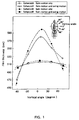
- FIGs. 1 and 2 shows results of measurement on the film thickness distribution for the spheroids A and B, where a spin motion was performed alone or together with a swing motion.
- the distance between the flat plate target surface and the rotational axis of spheroids (light bulb filaments) was set to be 90mm.
- FIG. 1 shows the thickness distribution of a film formed on spheroids of light bulbs in the rotational axis direction.
- FIG. 1 shows also a measurement result as a comparative example obtained by forming a film using only a spin motion but not a swing motion.
- FIG. 2 shows a thickness distribution of a film in the direction of the cross-sectional circumferential direction (spin rotational direction) perpendicular to the rotational axis.
- the ordinate in FIG. 1 indicates thickness (nm) of an SiO 2 film.
- the abscissa indicates positions of a light bulb surface corresponding to vertical angles (elevation angle) of a surface that is perpendicular to the rotational axis of a spheroid comprising the midpoint P. For the vertical angle, the direction inverse to the light bulb terminals is determined to be the plus direction, while the light bulb terminal side is determined to be the minus direction (see upper right-hand in FIG. 1).
- the ordinate in FIG. 2 indicates thickness (nm) of an SiO 2 film.
- the abscissa indicates positions on the light bulb periphery on a surface perpendicular to the rotational axis of a spheroid including the midpoint P.
- the zero-degree direction is the position where a mount is provided to the filament on the rotational axis.
- the angles are displayed by determining the counterclockwise direction as the plus direction about the rotational axis relative to the zero-degree when viewed from the top of the light bulb (right-center in FIG. 2).
- FIGs. 1 and 2 show that films can be formed on light bulbs with a substantial uniformity in both the vertical and horizontal directions when a swing motion is performed together with a spin motion.
- the measurement result in FIG. 1 shows that additional use of a swing motion is remarkably effective when compared with the result obtained by using only a spin motion.
- the problem of uneven thickness of the thin film formed on a bulb cannot be solved by using a spin motion alone, especially when the thin film is formed with an incident particle beam coming from a particle source located in a specific direction when viewed from the object (e.g., RF sputtering).
- an SiO 2 thin film was formed on a light bulb surface by using RF sputtering as in the First Embodiment.
- This embodiment is distinguishable from the First Embodiment in that the swing motion is not a continuous motion as shown in FIG. 4 but an intermittent motion as shown in FIG. 6 (hereinafter, it is called "a step-swing mode").
- an oscillation angular range of a rotational oscillation in a swing motion of a predetermined cycle is divided to be set as plural stationary angles ( ⁇ n ), and stationary times (tn) for the respective stationary angular positions are also set. More specifically, the rotational motion of the swing is set as ( ⁇ 1, t1)...( ⁇ n, tn) within the range of the amplitude angles.
- the step-swing mode can be provided in a simple manner compared to the continuous swing mode described in the First Embodiment.
- n 5
- the rotational angular range of the swing amplitude is set to be ⁇ 45 degrees to the medium value.
- the angular velocity for moving between the respective stationary angular positions can be constant or not.
- the velocity for moving between the respective stationary angular positions is substantially constant, and the time required for the move is short (within one second per step) when compared to the stationary time (tn) at each stationary angular position.
- FIG. 5 shows a comparison between an example using the step-swing mode in addition to a spin motion, and a comparative example using a spin motion alone.
- Both the example and comparative example include SiO 2 thin films formed on light bulbs by using RF sputtering as in the First Embodiment.
- light bulbs having spheroid A were used.
- the target was a flat plate 200mm in width and 900mm in length.
- the spin motion the spheroid rotates about the axis of the filament at a regular angular velocity of 100rpm.
- FIG. 5 shows that a step-swing mode can provide a uniform film thickness as in the case of a continuous swing mode. The effect is further remarkable when compared with a comparative example of a film formed by using a spin motion alone.
- the film-forming methods in the embodiments provide thin films with a uniform thickness. Therefore, the method for forming films of the present invention is useful in forming interference infrared reflection multilayer films or frost films on light bulbs.
- Such multilayer films comprise laminates of transparent dielectric multilayer films differing in the refractive indices.
- a 90W tungsten-halogen lamp including a light bulb having a spheroid was prepared by forming an infrared reflection thin film on the spheroid by using a method in the present invention. This lamp was used for a comparison with a tungsten-halogen lamp having the identical total value of luminous flux (1600 lumen) prepared without using the method of the present invention. The efficiency of the present invention (1m/W) was improved by about 30%.
- RF sputtering was used for forming thin films in the embodiments.
- the film-forming method is not limited thereto as long as the thin films are formed with an incident particle beam coming from a particle source located in a specific direction when viewed from the substrates. Equivalent effects are obtainable in any other general-purpose sputtering such as DC sputtering, or various kinds of evaporation.
- Thin films in the above-identified embodiments can be formed by using film-formation equipment having a rotational mechanism for performing a spin motion together with a swing motion, and by combining the film-forming method with conventional evaporation or sputtering.
- a thin film with a uniform thickness can be formed with accurate control on a substrate even when incident sputtered particles are supplied from only a specific direction as in a conventional method such as evaporation and sputtering, or even when the substrate comprises a spheroid such as a light bulb.
Landscapes
- Chemical & Material Sciences (AREA)
- Engineering & Computer Science (AREA)
- Manufacturing & Machinery (AREA)
- Chemical Kinetics & Catalysis (AREA)
- Materials Engineering (AREA)
- Mechanical Engineering (AREA)
- Metallurgy (AREA)
- Organic Chemistry (AREA)
- Physical Vapour Deposition (AREA)
- Formation Of Various Coating Films On Cathode Ray Tubes And Lamps (AREA)
- Physical Deposition Of Substances That Are Components Of Semiconductor Devices (AREA)
Applications Claiming Priority (2)
| Application Number | Priority Date | Filing Date | Title |
|---|---|---|---|
| JP10244299A JP3506949B2 (ja) | 1999-04-09 | 1999-04-09 | 薄膜の製造方法、薄膜が形成された回転楕円体、及びこれを用いた電球と薄膜形成装置。 |
| JP10244299 | 1999-04-09 |
Publications (2)
| Publication Number | Publication Date |
|---|---|
| EP1043418A2 true EP1043418A2 (de) | 2000-10-11 |
| EP1043418A3 EP1043418A3 (de) | 2003-03-12 |
Family
ID=14327592
Family Applications (1)
| Application Number | Title | Priority Date | Filing Date |
|---|---|---|---|
| EP00107104A Withdrawn EP1043418A3 (de) | 1999-04-09 | 2000-04-06 | Verfahren zum Herstellen einer Dünnschicht |
Country Status (5)
| Country | Link |
|---|---|
| US (3) | US6472022B1 (de) |
| EP (1) | EP1043418A3 (de) |
| JP (1) | JP3506949B2 (de) |
| CN (1) | CN100334684C (de) |
| CA (1) | CA2304028A1 (de) |
Cited By (1)
| Publication number | Priority date | Publication date | Assignee | Title |
|---|---|---|---|---|
| CN102555130A (zh) * | 2010-12-17 | 2012-07-11 | 中国科学院理化技术研究所 | 一种通过旋转容器成膜制备聚合物膜的方法 |
Families Citing this family (6)
| Publication number | Priority date | Publication date | Assignee | Title |
|---|---|---|---|---|
| JP3506949B2 (ja) * | 1999-04-09 | 2004-03-15 | 松下電器産業株式会社 | 薄膜の製造方法、薄膜が形成された回転楕円体、及びこれを用いた電球と薄膜形成装置。 |
| DE10196579T1 (de) * | 2000-09-07 | 2003-07-03 | Matsushita Electric Industrial Co Ltd | Verfahren zur Bildung eines Dünnfilms und Elektrolampe mit dem Dünnfilm |
| US8035285B2 (en) * | 2009-07-08 | 2011-10-11 | General Electric Company | Hybrid interference coatings, lamps, and methods |
| CN107723675A (zh) * | 2017-11-17 | 2018-02-23 | 东莞颠覆产品设计有限公司 | 物理气相沉积设备和物理气相沉积方法 |
| CN109234695A (zh) * | 2018-11-15 | 2019-01-18 | 杭州电子科技大学 | 一种纳米金属间化合物储氢材料的制备方法 |
| JP6635492B1 (ja) * | 2019-10-15 | 2020-01-29 | サンテック株式会社 | 基板回転装置 |
Family Cites Families (22)
| Publication number | Priority date | Publication date | Assignee | Title |
|---|---|---|---|---|
| US2946697A (en) * | 1957-12-31 | 1960-07-26 | Westinghouse Electric Corp | Masking method and apparatus |
| GB1208528A (en) * | 1968-07-01 | 1970-10-14 | Sylvania Electric Prod | Shatter-proof electric lamp |
| DE2813180C2 (de) * | 1978-03-25 | 1985-12-19 | Leybold-Heraeus GmbH, 5000 Köln | Vakuumbeschichtungsanlage zum allseitigen Beschichten von Substraten durch Rotation der Substrate im Materialstrom |
| US4851095A (en) | 1988-02-08 | 1989-07-25 | Optical Coating Laboratory, Inc. | Magnetron sputtering apparatus and process |
| JPH03232963A (ja) | 1990-02-08 | 1991-10-16 | Nippon Steel Corp | セラミックス膜被覆方法 |
| JPH07122132B2 (ja) * | 1990-11-01 | 1995-12-25 | 松下電器産業株式会社 | 薄膜形成方法および薄膜形成装置 |
| ATE147890T1 (de) | 1991-05-31 | 1997-02-15 | Deposition Sciences Inc | Sputteranlage |
| JPH06181048A (ja) | 1992-08-31 | 1994-06-28 | Toshiba Lighting & Technol Corp | 管球および管球への被膜形成方法 |
| JP3232963B2 (ja) | 1994-10-11 | 2001-11-26 | 株式会社日立製作所 | 有機基板接続用鉛レスはんだ及びそれを用いた実装品 |
| US5616224A (en) | 1995-05-09 | 1997-04-01 | Deposition Sciences, Inc. | Apparatus for reducing the intensity and frequency of arcs which occur during a sputtering process |
| US6309692B1 (en) * | 1996-01-22 | 2001-10-30 | Chugai Ro Co., Ltd. | Method of and apparatus for coating a substrate with a coating material having an even thickness |
| EP0854210B1 (de) * | 1996-12-19 | 2002-03-27 | Toshiba Ceramics Co., Ltd. | Aufdampfungsvorrichtung zur Herstellung von Dünnfilmen |
| US5925410A (en) * | 1997-05-06 | 1999-07-20 | Micron Technology, Inc. | Vibration-enhanced spin-on film techniques for semiconductor device processing |
| JP3424516B2 (ja) * | 1997-07-30 | 2003-07-07 | 松下電器産業株式会社 | ハロゲン電球およびその製造方法 |
| US6183810B1 (en) * | 1998-01-21 | 2001-02-06 | Tokyo Electron Limited | Coating film forming method and coating apparatus |
| US6159290A (en) * | 1998-10-02 | 2000-12-12 | Shamrock Technology Corp. | Apparatus for, and method of, providing controlled depositions on substrates |
| JP4187323B2 (ja) * | 1998-10-13 | 2008-11-26 | Tdk株式会社 | 真空成膜処理装置および方法 |
| US6352747B1 (en) * | 1999-03-31 | 2002-03-05 | Ppg Industries Ohio, Inc. | Spin and spray coating process for curved surfaces |
| JP3506949B2 (ja) * | 1999-04-09 | 2004-03-15 | 松下電器産業株式会社 | 薄膜の製造方法、薄膜が形成された回転楕円体、及びこれを用いた電球と薄膜形成装置。 |
| US6485616B1 (en) * | 1999-12-29 | 2002-11-26 | Deposition Sciences, Inc. | System and method for coating substrates with improved capacity and uniformity |
| US6303008B1 (en) * | 2000-09-21 | 2001-10-16 | Delphi Technologies, Inc. | Rotating film carrier and aperture for precision deposition of sputtered alloy films |
| US6395156B1 (en) * | 2001-06-29 | 2002-05-28 | Super Light Wave Corp. | Sputtering chamber with moving table producing orbital motion of target for improved uniformity |
-
1999
- 1999-04-09 JP JP10244299A patent/JP3506949B2/ja not_active Expired - Fee Related
-
2000
- 2000-03-29 US US09/537,622 patent/US6472022B1/en not_active Expired - Fee Related
- 2000-04-05 CA CA002304028A patent/CA2304028A1/en not_active Abandoned
- 2000-04-06 EP EP00107104A patent/EP1043418A3/de not_active Withdrawn
- 2000-04-07 CN CNB001065378A patent/CN100334684C/zh not_active Expired - Fee Related
-
2002
- 2002-09-09 US US10/238,092 patent/US6726816B2/en not_active Expired - Fee Related
- 2002-09-09 US US10/238,087 patent/US6635330B2/en not_active Expired - Fee Related
Cited By (1)
| Publication number | Priority date | Publication date | Assignee | Title |
|---|---|---|---|---|
| CN102555130A (zh) * | 2010-12-17 | 2012-07-11 | 中国科学院理化技术研究所 | 一种通过旋转容器成膜制备聚合物膜的方法 |
Also Published As
| Publication number | Publication date |
|---|---|
| JP2000294200A (ja) | 2000-10-20 |
| CN100334684C (zh) | 2007-08-29 |
| US6726816B2 (en) | 2004-04-27 |
| EP1043418A3 (de) | 2003-03-12 |
| JP3506949B2 (ja) | 2004-03-15 |
| US6472022B1 (en) | 2002-10-29 |
| CA2304028A1 (en) | 2000-10-09 |
| US6635330B2 (en) | 2003-10-21 |
| US20030008146A1 (en) | 2003-01-09 |
| CN1277457A (zh) | 2000-12-20 |
| US20030012886A1 (en) | 2003-01-16 |
Similar Documents
| Publication | Publication Date | Title |
|---|---|---|
| US3271179A (en) | Method for the manufacture of an optical filter | |
| US4954756A (en) | Method and apparatus for changing the emission characteristics of an electrodeless lamp | |
| US6472022B1 (en) | Method for forming thin film, spheroid coated with thin film, light bulb using the spheroid and equipment for film formation | |
| CN100561331C (zh) | 光源装置和使用该光源装置的图像显示装置 | |
| CN103912848A (zh) | 一种利用漫反射基板进行光学设计的荧光粉色轮及其制作方法 | |
| US4173778A (en) | Lighting fixtures and glass enclosure having high angle anti-reflection coating | |
| JP2006133331A (ja) | 光反射鏡、その製造方法およびプロジェクター | |
| JPS62103602A (ja) | 光源装置 | |
| CN203810291U (zh) | 一种利用漫反射基板进行光学设计的荧光粉色轮 | |
| US4812957A (en) | Optical system for uniform illumination of a plane surface | |
| US6911125B2 (en) | Thin film producing method and light bulb having such thin film | |
| CA2043272C (en) | Projection cathode-ray tube | |
| CA2049491C (en) | Projection cathode-ray tube with uniform optical multiple interference film | |
| JPS62103962A (ja) | 白熱電灯 | |
| JP2001243924A (ja) | 管球および反射鏡付管球 | |
| WO2019230936A1 (ja) | 光学素子、車両用前照灯具、光源装置、および投影装置 | |
| JP2724648B2 (ja) | 照明灯及びその反射面の形成方法 | |
| CN213712775U (zh) | 一种控光装置及投光灯 | |
| JP3384055B2 (ja) | 真空薄膜形成装置 | |
| JP2829730B2 (ja) | 無電極ランプの射出特性を変化させる方法及び装置 | |
| Omata et al. | Sputtering deposition of infra-red reflecting films on ellipsoidal bulbs of energy saving lamps | |
| JPH08111105A (ja) | 多層膜反射鏡 | |
| JP3667374B2 (ja) | 照明装置 | |
| JPH08273415A (ja) | 反射鏡付光源 | |
| JP2006301232A (ja) | 光反射鏡、その製造方法およびプロジェクター |
Legal Events
| Date | Code | Title | Description |
|---|---|---|---|
| PUAI | Public reference made under article 153(3) epc to a published international application that has entered the european phase |
Free format text: ORIGINAL CODE: 0009012 |
|
| AK | Designated contracting states |
Kind code of ref document: A2 Designated state(s): AT BE CH CY DE DK ES FI FR GB GR IE IT LI LU MC NL PT SE |
|
| AX | Request for extension of the european patent |
Free format text: AL;LT;LV;MK;RO;SI |
|
| RAP1 | Party data changed (applicant data changed or rights of an application transferred) |
Owner name: MATSUSHITA ELECTRIC INDUSTRIAL CO., LTD. |
|
| RAP1 | Party data changed (applicant data changed or rights of an application transferred) |
Owner name: MATSUSHITA ELECTRIC INDUSTRIAL CO., LTD. |
|
| PUAL | Search report despatched |
Free format text: ORIGINAL CODE: 0009013 |
|
| AK | Designated contracting states |
Kind code of ref document: A3 Designated state(s): AT BE CH CY DE DK ES FI FR GB GR IE IT LI LU MC NL PT SE Designated state(s): AT BE CH CY DE DK ES FI FR GB GR IE IT LI LU MC NL PT SE |
|
| AX | Request for extension of the european patent |
Extension state: AL LT LV MK RO SI |
|
| RIC1 | Information provided on ipc code assigned before grant |
Ipc: 7H 01J 9/20 B Ipc: 7H 01J 63/04 B Ipc: 7H 01K 3/00 B Ipc: 7C 23C 14/50 A |
|
| 17P | Request for examination filed |
Effective date: 20030327 |
|
| AKX | Designation fees paid |
Designated state(s): DE GB NL |
|
| 17Q | First examination report despatched |
Effective date: 20070510 |
|
| STAA | Information on the status of an ep patent application or granted ep patent |
Free format text: STATUS: THE APPLICATION HAS BEEN WITHDRAWN |
|
| 18W | Application withdrawn |
Effective date: 20080429 |