EP1035548B1 - Synchronous semiconductor memory device - Google Patents
Synchronous semiconductor memory device Download PDFInfo
- Publication number
- EP1035548B1 EP1035548B1 EP00104469A EP00104469A EP1035548B1 EP 1035548 B1 EP1035548 B1 EP 1035548B1 EP 00104469 A EP00104469 A EP 00104469A EP 00104469 A EP00104469 A EP 00104469A EP 1035548 B1 EP1035548 B1 EP 1035548B1
- Authority
- EP
- European Patent Office
- Prior art keywords
- data
- bits
- data line
- lines
- transferred
- Prior art date
- Legal status (The legal status is an assumption and is not a legal conclusion. Google has not performed a legal analysis and makes no representation as to the accuracy of the status listed.)
- Expired - Lifetime
Links
- 230000001360 synchronised effect Effects 0.000 title claims description 15
- 239000004065 semiconductor Substances 0.000 title claims description 14
- 230000002093 peripheral effect Effects 0.000 claims description 49
- 239000000872 buffer Substances 0.000 claims description 47
- 230000003213 activating effect Effects 0.000 claims description 16
- 230000000295 complement effect Effects 0.000 claims description 7
- 238000010276 construction Methods 0.000 claims description 7
- 239000007787 solid Substances 0.000 claims description 2
- 238000010586 diagram Methods 0.000 description 8
- 238000000034 method Methods 0.000 description 4
- 238000010008 shearing Methods 0.000 description 4
- 230000003247 decreasing effect Effects 0.000 description 2
- VLQGDKKHHCKIOJ-UHFFFAOYSA-N NNOS Chemical compound NNOS VLQGDKKHHCKIOJ-UHFFFAOYSA-N 0.000 description 1
- 230000004913 activation Effects 0.000 description 1
- 238000006243 chemical reaction Methods 0.000 description 1
- 230000001419 dependent effect Effects 0.000 description 1
- 230000000694 effects Effects 0.000 description 1
- 230000004044 response Effects 0.000 description 1
- 230000001960 triggered effect Effects 0.000 description 1
Images


Classifications
-
- G—PHYSICS
- G11—INFORMATION STORAGE
- G11C—STATIC STORES
- G11C11/00—Digital stores characterised by the use of particular electric or magnetic storage elements; Storage elements therefor
- G11C11/21—Digital stores characterised by the use of particular electric or magnetic storage elements; Storage elements therefor using electric elements
- G11C11/34—Digital stores characterised by the use of particular electric or magnetic storage elements; Storage elements therefor using electric elements using semiconductor devices
- G11C11/40—Digital stores characterised by the use of particular electric or magnetic storage elements; Storage elements therefor using electric elements using semiconductor devices using transistors
- G11C11/41—Digital stores characterised by the use of particular electric or magnetic storage elements; Storage elements therefor using electric elements using semiconductor devices using transistors forming static cells with positive feedback, i.e. cells not needing refreshing or charge regeneration, e.g. bistable multivibrator or Schmitt trigger
- G11C11/413—Auxiliary circuits, e.g. for addressing, decoding, driving, writing, sensing, timing or power reduction
-
- G—PHYSICS
- G11—INFORMATION STORAGE
- G11C—STATIC STORES
- G11C7/00—Arrangements for writing information into, or reading information out from, a digital store
- G11C7/10—Input/output [I/O] data interface arrangements, e.g. I/O data control circuits, I/O data buffers
- G11C7/1051—Data output circuits, e.g. read-out amplifiers, data output buffers, data output registers, data output level conversion circuits
- G11C7/106—Data output latches
-
- G—PHYSICS
- G11—INFORMATION STORAGE
- G11C—STATIC STORES
- G11C7/00—Arrangements for writing information into, or reading information out from, a digital store
- G11C7/10—Input/output [I/O] data interface arrangements, e.g. I/O data control circuits, I/O data buffers
- G11C7/1015—Read-write modes for single port memories, i.e. having either a random port or a serial port
- G11C7/1039—Read-write modes for single port memories, i.e. having either a random port or a serial port using pipelining techniques, i.e. using latches between functional memory parts, e.g. row/column decoders, I/O buffers, sense amplifiers
-
- G—PHYSICS
- G11—INFORMATION STORAGE
- G11C—STATIC STORES
- G11C7/00—Arrangements for writing information into, or reading information out from, a digital store
- G11C7/10—Input/output [I/O] data interface arrangements, e.g. I/O data control circuits, I/O data buffers
- G11C7/1051—Data output circuits, e.g. read-out amplifiers, data output buffers, data output registers, data output level conversion circuits
- G11C7/1066—Output synchronization
-
- G—PHYSICS
- G11—INFORMATION STORAGE
- G11C—STATIC STORES
- G11C7/00—Arrangements for writing information into, or reading information out from, a digital store
- G11C7/10—Input/output [I/O] data interface arrangements, e.g. I/O data control circuits, I/O data buffers
- G11C7/1072—Input/output [I/O] data interface arrangements, e.g. I/O data control circuits, I/O data buffers for memories with random access ports synchronised on clock signal pulse trains, e.g. synchronous memories, self timed memories
-
- G—PHYSICS
- G11—INFORMATION STORAGE
- G11C—STATIC STORES
- G11C7/00—Arrangements for writing information into, or reading information out from, a digital store
- G11C7/22—Read-write [R-W] timing or clocking circuits; Read-write [R-W] control signal generators or management
-
- G—PHYSICS
- G11—INFORMATION STORAGE
- G11C—STATIC STORES
- G11C2207/00—Indexing scheme relating to arrangements for writing information into, or reading information out from, a digital store
- G11C2207/10—Aspects relating to interfaces of memory device to external buses
- G11C2207/107—Serial-parallel conversion of data or prefetch
Definitions
- the present invention relates generally to a synchronous semiconductor memory device wherein a data transfer is carried out in synchronism with a clock. More specifically, the invention relates to an internal data transfer system in a DDR synchronous DRAM and so on wherein a pre-fetch system for a plurality of bits of data is used.
- SDRAMs synchronous DRAMs
- the SDRAMs are practicable from 4-Mbit DRAMs, and account for most of the current 64-Mbit DRAMs.
- the SDRAMs are characterized in that a rapid access time and cycle time are realized by utilizing a clock synchronization. Recently, it is requested to further accelerate the SDRAMs.
- the operating speed of an SDRAM is determined by a series of data transfer operations for transferring data, which are read out to bit lines of a memory cell array, to a main data line via a column selecting gate to amplify the transferred data to transfer the amplified data to an input/output terminal via a peripheral data line.
- a plurality of bits of data per I/O terminal are simultaneously read from the memory cell array to be parallel-to-serial converted by a peripheral circuit to be fetched.
- This technique is called a data pre-fetch, which will be hereinafter referred to as a 2-bit pre-fetch when 2-bit data per I/O terminal are simultaneously read out, and as a 4-bit pre-fetch when 4-bit data per I/O terminal are simultaneously read out.
- 2-bit data parallel-transferred to a data line via a column selecting line are amplified by data line buffers, respectively, to be transferred to separate peripheral data lines.
- the order in which the 2-bit data parallel-transferred to the peripheral data lines are fetched is determined in accordance with the least significant column address A0, so that the 2-bit data are parallel-to-serial converted to be fetched.
- the main current of the clock frequencies of SDRAMs is in the range of from 100 MHz to 133 MHz. If the above described data pre-fetch system is adopted by a technique for carrying out a column selection in a clock cycle to synchronize output data with both of leading and trailing edges of a clock or synchronize output data with an intersecting time between a clock CLK and a complementary clock /CLK thereto, it is possible to realize a data transfer speed of 200 MHz to 266 MHz twice as large as the clock frequency (DDR SDRAM).
- the number of peripheral data lines is twice as large as that when any pre-fetch systems are adopted.
- the number of required peripheral data lines is 32, and in the case of 32-bit parallel readout, the number of required peripheral data lines is 64.
- the rate of the area occupied by a memory cell array increases, so that the influence of the increased number of peripheral data lines is relatively decreased.
- the area occupied by the peripheral data lines can not be ignored, so that there is a default-like overhead with respect to a conventional DRAM which does not adopt the pre-fetch system.
- US-5,784,705 describes a method and structure for performing pipeline burst accesses in a semiconductor memory.
- a memory bank is shown that comprises a DRAM cell array, a word line driver, a bank select circuit, a plurality of sense amplifiers and column select switches.
- a read data buffer is provided, which comprises a data amplifier circuit that receives data signals from the column select switches and is connected to a transparent latch circuit.
- the transparent latch circuit is connected to a multiplexer, which in turn is connected to an I/O device.
- the transparent latch circuit is enabled by a transfer enable signal which is generated by a write/read buffer control circuit.
- the multiplexer sequentially routes data words from the transparent latch circuit to the I/O device in response to a burst access signal generated by a burst access sequencer.
- FIG. 1 is a block diagram of a preferred embodiment of a DDR SDRAM according to the present invention.
- a DRAM core 1 includes a memory cell array 2, a row decoder 3 and column decoder 4 for selecting a word line and bit line of the memory cell array 2, and a bit line sense amplifier 5 for amplifying bit line data.
- An external clock CLK is incorporated by a clock buffer 11 to produce an internal clock.
- a command decoder 6 decodes a command ACT for indicating the readout/writing of data from the outside.
- a control signal generating circuit 7 generates various control signals, such as a sense amplifier activating signal which is timing-controlled by the internal clock.
- An address buffer 8 incorporates an address ADD in synchronism with the internal clock to transmit a row address and a column address to the row decoder 3 and the column decoder 4, respectively.
- the data read out of the DRAM core 1 to be transferred to a main data line MDQ are amplified by a data line buffer 9.
- the data amplified by the data line buffer 9 are transferred to a peripheral data line RD to be fetched to an I/O terminal via an I/O buffer 10 which is controlled by the internal clock.
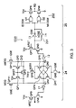
- FIG. 2 shows the construction of a principal part relating to the data transfer from the DRAM core 1 to the I/O terminal by taking notice of one peripheral data line RD when a 2-bit pre-fetch system is adopted.
- the number of peripheral data lines RD is also 16 in the case of a solid wire.
- FIG. 2 shows one cell block 21 of the memory cell array 2 usually comprising a plurality of cell blocks. As shown in this figure, in the cell block 21, a plurality of word lines WL and a plurality of bit line pairs BL and bBL intersecting the work lines WL are formed, and dynamic memory cells MC are arranged at the intersections therebetween.
- a plurality of main data line pairs MDQ and bMDQ are provided.
- main data line pairs two pairs of main data lines MDQ(E), bMDQ(E) and MDQ (O), bMDQ(O) corresponding to 2-bit data read out in parallel are shown in FIG. 2.
- These two pairs of main data lines hold one peripheral data line RD in common.
- the bit line data of the cell block 21 are amplified by the bit line sense amplifier 5 to be transferred to the main bit line pair MDQ, bMDQ via column selecting gates 22, 23 driven by a column selection signal CSL.
- the end portions of the main data line pair MDQ, bMDQ are provided with data line buffers DQB(E), DQB(O) contained in the data line buffer 9 of FIG. 1, respectively.
- two column selecting lines CSL(E), CSL(O) shown as an example are simultaneously selected in synchronism with a clock, so that 2-bit bit line data are simultaneously transferred to the main data line pairs MDQ(E), bMDQ(E) and MDQ(O), bMDQ(O) to be amplified by the data line buffers DQB(E) and DQB(O). That is, although the 2-bit pre-fetch operation is carried out, the 2-bit data are transferred to one peripheral data line RD in a time sharing operation unlike the conventional system. For that reason, each of the data line buffers DQB comprises a sense amplifier 24, and a latch circuit 25 serving as a cache for temporarily holding data which are amplified by the sense amplifier 24.
- the data transferred to the peripheral data line RD are fetched to the I/O terminal via a FIFO buffer 26 and the I/O buffer 10.
- the FIFO buffer 26 may be a well known FIFO buffer shown in FIG. 7.
- FIG. 3 shows an example of one data line buffer DQB.
- the sense amplifier 24 has a flip-flop type sense amplifier body 241 which comprises PMOS transistors QP4, QP5 and NMOS transistors QN1, QN2.
- the sense amplifier body 241 has an activating PMOS transistor QP6 and an activating NMOS transistor QN5 on the side of a power supply and the ground, respectively.
- the activating PMOS transistor QN5 and the activating NNOS transistor QP6 are driven by complementary activating signals QSE and bQSE, respectively, which are timing-controlled by clocks.
- a transfer gate comprising PMOS transistors QP11 and QP12 is provided between the main data line pair MDQ, bMDQ and sense nodes N1, N2, a transfer gate comprising PMOS transistors QP11 and QP12 is provided. This transfer gate is controlled by a sense amplifier activating signal QSE, and is turned off during the activation of the sense amplifier 241, so that the data line pair MDQ and bMDQ is
- a data line equalizer circuit 242 comprising PMOS transistors QP1, QP2 and QP3 is provided.
- One sense node N1 is connected, via an inverter I1, to the gate of a dummy NMOS transistor QN6, the drain of which is connected to a pre-charging PMOS transistor QP9, which is controlled by a reset signal (pre-charge signal) bRST, to be terminated.
- the other sense node N2 is connected, via an inverter I2, to the gate of an output NMOS transistor QN3, the drain of which is connected to a pre-charging PMOS transistor QP7.
- the latch circuit 25 has a latch circuit body 251, to which the activating signals QSE and bQSE are directly supplied as latch signals.
- the latch circuit body 251 comprises inverters I3 and I4, the inputs/outputs of which are cross-connected.
- the data of the latch circuit body 251 are transferred to a peripheral data line RD via a driver 252 which is controlled by complementary control signals EOSW and bEOSWwhich are in "H” or "L” in synchronism with the least significant column address CA0.
- the driver 252 comprises a PMOS transistor QP8 controlled by the output of a two-input NAND gate G1, to which the output of the latch circuit body 251 and the control signal EOSW are inputted, and an NMOS transistor QN4 controlled by the output of a two-input NOR gate G2, to which the output of the latch circuit body 251 and the control signal bEOSW are inputted.
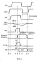
- FIG. 4 is a timing chart for a data transfer operation in this preferred embodiment.
- a reset signal bRST is in "H", so that the pre-charge period of the sense amplifier 24 of the data line buffer DQB expires.
- the PMOS transistors QP1, QP2 and QP3 of the equalizer circuit 242 remain being turned on, so that the sense nodes N1 and N2 are pre-charged to VCC.
- the PMOS transistors QP7 and QP9 are turned on, so that the drain nodes of the NMOS transistors QN6 and QN3 are pre-charged to VCC.
- bit line data are transferred to the main data line pair MDQ and bMDQ, so that a voltage difference occurs in accordance with the data as shown in the figure.
- 2-bit data per one I/O terminal are simultaneously transferred to the main data line pair as described above.
- an activating signal QSE of the data line sense amplifier rises, and a complementary signal bQSE thereto is in "L".
- a complementary signal bQSE thereto is in "L”.
- one of the sense nodes N1 and N2 is changed to VCC, and the other is changed to VSS.
- the data of the node N2 are inverted by the inverter I2, and inverted by the NMOS transistor QN3 again to be transferred to the latch circuit body 251.
- the latch circuit body 251 receives the sense amplifier activating signals QSE and bQSE as latch signals to incorporate the transferred data.
- a control signal EOSW(E) generated in synchronism with the least significant column address CA0 rises at time t3.
- data transferred to the latch circuit body 251 on the side of the data line pair MDQ(E) and bMDQ(E) are transferred to the peripheral data line RD via the driver 252 as head data D(E).
- the control signal EOSW(O) is in "L” and bEOSW(O) is in "H", so that the gates G1 and G2 of the driver 252 remain being closed. Therefore, subsequent data are temporarily held in the latch circuit body 251.
- the sense amplifier activating signal QSE is in "L” at time t4.
- the reset signal bRST is in "L"
- the sense amplifier 24 starts a pre-charge operation.
- the control signal EOSW(O) is in "H” and bEOSW(O) is in "L”
- the subsequent data D(O) held in the latch circuit body 25 are transferred to the peripheral data line RD via the driver 252.
- the head data previously transferred at the trailing edge of the clock CLK are incorporated by the FIFO buffer 26.
- the 2-bit data pre-fetched to the data line buffer are sequentially transferred to the common peripheral data line RD by the time sharing operation.
- the time for the subsequent data to be latched is substantially half of the clock frequency.
- the 2-bit data serially transferred to the peripheral data line RD in the time shearing operation are fetched from the same I/O terminal via, e.g., the FIFO buffer 26 triggered at both edges of the clock CLK, and the I/O buffer 9.
- the head data pass through the data line buffer, and the subsequent data are temporarily held be transferred to the common peripheral data line. Therefore, the number of the peripheral data lines can be reduced to half of that in the conventional pre-fetch system.
- the effect of reducing the number of the peripheral data lines is great, so that it is possible to reduce the chip size.
- the parallel-to-serial conversion is carried out by the data transfer operation from the data line buffer to the peripheral data line, so that it is not required to provide any parallel-to-serial converter circuits unlike the conventional pre-fetch system.
- the latch circuit 25 operates using the activating signal of the data line sense amplifier 24 as the latch signal. Therefore, while the subsequent data are held by the latch circuit 25, the sense amplifier activating signal QSE being the latch signal is in "L". In this stage, the data line sense amplifier 24 starts the pre-charge operation for the next cycle. That is, since the pre-charge operation of the data buffer and the data latch operation can temporally overlap each other, a useless clock cycle is not used by adding the latch circuit, so that it is possible to prevent the cycle time from increasing.
- FIG. 5 shows the construction of a principal part of another preferred embodiment of an SDRAM according to the present invention, which corresponds to FIG. 2.
- the peripheral data line to which 2-bit data are transferred in a time shearing operation, comprises complementary signal lines RD and bRD similar to the main data line.
- Other constructions are the same as those in the preceding preferred embodiment.
- the number of the peripheral data lines is double as large as that in the preceding preferred embodiment. However, the number of the peripheral data lines is reduced to half of that when the pre-fetched 2-bit data are transferred to the peripheral data lines having the construction of complementary signal lines in parallel.
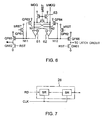
- FIG. 6 is a circuit diagram of a sense amplifier circuit of a data line buffer circuit in another preferred embodiment.
- This data line sense amplifier mainly comprises current mirror type differential amplifiers 61 and 62.
- One input nodes of the differential amplifiers 61 and 62 are sense nodes N1 and N2 which are connected to main data lines MDQ and bMDQ.
- an equalizer circuit 62 is provided similar to the case of FIG. 3.
- the output nodes N11 and N12 of the differential amplifiers 61 and 62 are connected to the gates of PMOS transistors QP63 and QP64, the drains of which are connected to the sense nodes N2 and N1, respectively.
- the PMOS transistors QP63 and QP64 serve to feed back the variation in potential of the output nodes N11 and N12 to the sense nodes N1 and N2 to accelerate the sense operation.
- PMOS transistors QP61 and QP62 connected to the output nodes N11 and N12 are provided for pre-charge.
- One output node N11 is terminated via an output driver comprising a PMOS transistor QP65 and an NMOS transistor QN62, and the other output node N12 is connected to a latch circuit via an output driver comprising a PMOS transistor QP66 and an NMOS transistor QN61 similar to the preceding preferred embodiment.
- a control signal bRST is in "L” and a control signal RST is in "H” during a pre-charge operation.
- the sense nodes N1 and N2 and the output nodes N11 and N12 are pre-charged to VCC.
- the output of the output driver is in "L”.
- the PMOS transistor QP66 of the output driver is turned on, so that an "H" level output is transmitted to the latch circuit.
- a plurality of bits of data can be generally transferred to the main data lines in parallel to be transferred to the common data line in the time shearing operation.
- the number of the peripheral data lines can be further decreased.
- FIG. 2A shows a substantial part of an example of the above, where 4-bit data pre-fetch is performed.
- each one bit data from each data line buffer DQB of four data line buffers DQB is transferred to a peripheral data line RD on the basis of the least significant column address CA0 and the adjacent column address CA1.
- each data is output from each of four data line buffers as shown in the table below.
- Table CASE CA0 CA1 output order of DQB 1 0 0 (0) ⁇ (1) ⁇ (2) ⁇ (3) 2 1 0 (1) ⁇ (2) ⁇ (3) ⁇ (0) 3 0 1 (2) ⁇ (3) ⁇ (0) ⁇ (1) 4 1 1 (3) ⁇ (0) ⁇ (1) ⁇ (2)
- n column address bits of the least significant bit side are used.
- Each data is transferred to a peripheral data line RD on the basis of a control signal obtained from the above n bits of column address.
Landscapes
- Engineering & Computer Science (AREA)
- Microelectronics & Electronic Packaging (AREA)
- Computer Hardware Design (AREA)
- Dram (AREA)
Applications Claiming Priority (2)
| Application Number | Priority Date | Filing Date | Title |
|---|---|---|---|
| JP6044099 | 1999-03-08 | ||
| JP11060440A JP2000260181A (ja) | 1999-03-08 | 1999-03-08 | 同期型半導体記憶装置 |
Publications (2)
| Publication Number | Publication Date |
|---|---|
| EP1035548A1 EP1035548A1 (en) | 2000-09-13 |
| EP1035548B1 true EP1035548B1 (en) | 2008-01-23 |
Family
ID=13142344
Family Applications (1)
| Application Number | Title | Priority Date | Filing Date |
|---|---|---|---|
| EP00104469A Expired - Lifetime EP1035548B1 (en) | 1999-03-08 | 2000-03-08 | Synchronous semiconductor memory device |
Country Status (6)
| Country | Link |
|---|---|
| US (1) | US6163501A (enExample) |
| EP (1) | EP1035548B1 (enExample) |
| JP (1) | JP2000260181A (enExample) |
| KR (1) | KR100368368B1 (enExample) |
| DE (1) | DE60037846T2 (enExample) |
| TW (1) | TW466482B (enExample) |
Families Citing this family (18)
| Publication number | Priority date | Publication date | Assignee | Title |
|---|---|---|---|---|
| KR100499623B1 (ko) * | 1998-12-24 | 2005-09-26 | 주식회사 하이닉스반도체 | 내부 명령신호 발생장치 및 그 방법 |
| DE19934500C2 (de) * | 1999-07-22 | 2001-10-31 | Infineon Technologies Ag | Synchroner integrierter Speicher |
| US6392935B1 (en) * | 2000-04-03 | 2002-05-21 | Maxtor Corporation | Maximum bandwidth/minimum latency SDRAM interface |
| KR100372247B1 (ko) * | 2000-05-22 | 2003-02-17 | 삼성전자주식회사 | 프리페치 동작모드를 가지는 반도체 메모리 장치 및 메인데이터 라인수를 줄이기 위한 데이터 전송방법 |
| US6756823B1 (en) * | 2000-06-28 | 2004-06-29 | Intel Corporation | Differential sense latch scheme |
| JP4684394B2 (ja) * | 2000-07-05 | 2011-05-18 | エルピーダメモリ株式会社 | 半導体集積回路装置 |
| JP4514945B2 (ja) * | 2000-12-22 | 2010-07-28 | 富士通セミコンダクター株式会社 | 半導体装置 |
| US6515914B2 (en) * | 2001-03-21 | 2003-02-04 | Micron Technology, Inc. | Memory device and method having data path with multiple prefetch I/O configurations |
| KR100468719B1 (ko) * | 2002-01-11 | 2005-01-29 | 삼성전자주식회사 | N 비트 프리페치 방식과 2n 버스트 길이를 지원할 수있는 반도체 메모리 장치 |
| US20030182208A1 (en) * | 2002-03-19 | 2003-09-25 | Eloda Inc. | Method and system for assisting consumer decision making and providing on-demand viewing access to broadcast and rich media ads |
| US6678201B2 (en) * | 2002-04-08 | 2004-01-13 | Micron Technology, Inc. | Distributed FIFO in synchronous memory |
| DE10260647B3 (de) * | 2002-12-23 | 2004-08-26 | Infineon Technologies Ag | Integrierter Halbleiterspeicher, insbesondere DRAM-Speicher, und Verfahren zum Betrieb desselben |
| WO2005045846A1 (ja) * | 2003-11-06 | 2005-05-19 | International Business Machines Corporation | 半導体記憶装置及びそのバースト動作方法 |
| KR20110088947A (ko) * | 2010-01-29 | 2011-08-04 | 주식회사 하이닉스반도체 | 반도체 메모리의 데이터 출력 회로 |
| US10025532B2 (en) * | 2015-09-11 | 2018-07-17 | Sandisk Technologies Llc | Preserving read look ahead data in auxiliary latches |
| US10642513B2 (en) | 2015-09-11 | 2020-05-05 | Sandisk Technologies Llc | Partially de-centralized latch management architectures for storage devices |
| TWI749823B (zh) * | 2020-10-23 | 2021-12-11 | 美商矽成積體電路股份有限公司 | 內部鎖存器電路及其鎖存信號產生方法 |
| KR20240177547A (ko) | 2023-06-20 | 2024-12-27 | 나영호 | 정화통을 구비한 용접 마스크 |
Family Cites Families (7)
| Publication number | Priority date | Publication date | Assignee | Title |
|---|---|---|---|---|
| JP3599334B2 (ja) * | 1991-08-16 | 2004-12-08 | マルティチップ テクノロジー, インコーポレイテッド | 高性能ダイナミックメモリシステム |
| JP2907074B2 (ja) * | 1995-08-25 | 1999-06-21 | 日本電気株式会社 | 半導体記憶装置 |
| JP3351692B2 (ja) * | 1995-09-12 | 2002-12-03 | 株式会社東芝 | シンクロナス半導体メモリ装置 |
| JP2817679B2 (ja) * | 1995-09-20 | 1998-10-30 | 日本電気株式会社 | 半導体メモリ |
| US5784705A (en) * | 1996-07-15 | 1998-07-21 | Mosys, Incorporated | Method and structure for performing pipeline burst accesses in a semiconductor memory |
| US6011748A (en) * | 1996-10-03 | 2000-01-04 | Credence Systems Corporation | Method and apparatus for built-in self test of integrated circuits providing for separate row and column addresses |
| JP4221764B2 (ja) * | 1997-04-25 | 2009-02-12 | 沖電気工業株式会社 | 半導体記憶装置 |
-
1999
- 1999-03-08 JP JP11060440A patent/JP2000260181A/ja active Pending
-
2000
- 2000-03-07 TW TW089104020A patent/TW466482B/zh not_active IP Right Cessation
- 2000-03-07 KR KR10-2000-0011203A patent/KR100368368B1/ko not_active Expired - Fee Related
- 2000-03-08 EP EP00104469A patent/EP1035548B1/en not_active Expired - Lifetime
- 2000-03-08 US US09/520,720 patent/US6163501A/en not_active Expired - Fee Related
- 2000-03-08 DE DE60037846T patent/DE60037846T2/de not_active Expired - Lifetime
Also Published As
| Publication number | Publication date |
|---|---|
| KR20000062766A (ko) | 2000-10-25 |
| JP2000260181A (ja) | 2000-09-22 |
| TW466482B (en) | 2001-12-01 |
| EP1035548A1 (en) | 2000-09-13 |
| DE60037846D1 (de) | 2008-03-13 |
| KR100368368B1 (ko) | 2003-01-24 |
| US6163501A (en) | 2000-12-19 |
| DE60037846T2 (de) | 2009-01-22 |
Similar Documents
| Publication | Publication Date | Title |
|---|---|---|
| EP1035548B1 (en) | Synchronous semiconductor memory device | |
| US6370068B2 (en) | Semiconductor memory devices and methods for sampling data therefrom based on a relative position of a memory cell array section containing the data | |
| JP2697634B2 (ja) | 同期型半導体記憶装置 | |
| US6859414B2 (en) | Data input device in semiconductor memory device | |
| US5535169A (en) | Semiconductor memory device | |
| US10534394B2 (en) | Apparatuses and methods for providing internal memory commands and control signals in semiconductor memories | |
| US6636444B2 (en) | Semiconductor memory device having improved data transfer rate without providing a register for holding write data | |
| JP4579304B2 (ja) | デバイスのタイミングを補償する装置及び方法 | |
| JP3778381B2 (ja) | 半導体メモリ装置 | |
| US6636443B2 (en) | Semiconductor memory device having row buffers | |
| US6795372B2 (en) | Bit line sense amplifier driving control circuits and methods for synchronous drams that selectively supply and suspend supply of operating voltages | |
| US6073219A (en) | Semiconductor memory device with high speed read-modify-write function | |
| US6456563B1 (en) | Semiconductor memory device that operates in sychronization with a clock signal | |
| US6345007B1 (en) | Prefetch and restore method and apparatus of semiconductor memory device | |
| US6341100B1 (en) | Semiconductor integrated circuit having circuit for writing data to memory cell | |
| US5986955A (en) | Method and apparatus for hiding data path equilibration time | |
| US6310808B1 (en) | Semiconductor memory device having structure for high-speed data processing | |
| JPH09167486A (ja) | メモリ装置 | |
| US5715210A (en) | Low power semiconductor memory device | |
| US6552954B2 (en) | Semiconductor integrated circuit device | |
| US5539693A (en) | Method of controlling semiconductor storage circuit | |
| JPH09251773A (ja) | 半導体記憶装置 | |
| US7075834B2 (en) | Semiconductor integrated circuit device | |
| JPH07326189A (ja) | 半導体記憶装置 | |
| JP2000090662A (ja) | 半導体集積回路 |
Legal Events
| Date | Code | Title | Description |
|---|---|---|---|
| PUAI | Public reference made under article 153(3) epc to a published international application that has entered the european phase |
Free format text: ORIGINAL CODE: 0009012 |
|
| 17P | Request for examination filed |
Effective date: 20000308 |
|
| AK | Designated contracting states |
Kind code of ref document: A1 Designated state(s): AT BE CH CY DE DK ES FI FR GB GR IE IT LI LU MC NL PT SE |
|
| AX | Request for extension of the european patent |
Free format text: AL;LT;LV;MK;RO;SI |
|
| RIN1 | Information on inventor provided before grant (corrected) |
Inventor name: OZAWA, SUSUMU, Inventor name: OHSHIMA, SHIGEO |
|
| AKX | Designation fees paid |
Free format text: DE FR GB |
|
| 17Q | First examination report despatched |
Effective date: 20041021 |
|
| GRAP | Despatch of communication of intention to grant a patent |
Free format text: ORIGINAL CODE: EPIDOSNIGR1 |
|
| GRAS | Grant fee paid |
Free format text: ORIGINAL CODE: EPIDOSNIGR3 |
|
| GRAA | (expected) grant |
Free format text: ORIGINAL CODE: 0009210 |
|
| AK | Designated contracting states |
Kind code of ref document: B1 Designated state(s): DE FR GB |
|
| REG | Reference to a national code |
Ref country code: GB Ref legal event code: FG4D |
|
| REF | Corresponds to: |
Ref document number: 60037846 Country of ref document: DE Date of ref document: 20080313 Kind code of ref document: P |
|
| PGFP | Annual fee paid to national office [announced via postgrant information from national office to epo] |
Ref country code: FR Payment date: 20080311 Year of fee payment: 9 |
|
| EN | Fr: translation not filed | ||
| PLBE | No opposition filed within time limit |
Free format text: ORIGINAL CODE: 0009261 |
|
| STAA | Information on the status of an ep patent application or granted ep patent |
Free format text: STATUS: NO OPPOSITION FILED WITHIN TIME LIMIT |
|
| 26N | No opposition filed |
Effective date: 20081024 |
|
| PG25 | Lapsed in a contracting state [announced via postgrant information from national office to epo] |
Ref country code: FR Free format text: LAPSE BECAUSE OF FAILURE TO SUBMIT A TRANSLATION OF THE DESCRIPTION OR TO PAY THE FEE WITHIN THE PRESCRIBED TIME-LIMIT Effective date: 20081114 |
|
| PGFP | Annual fee paid to national office [announced via postgrant information from national office to epo] |
Ref country code: GB Payment date: 20100303 Year of fee payment: 11 |
|
| PGFP | Annual fee paid to national office [announced via postgrant information from national office to epo] |
Ref country code: DE Payment date: 20100318 Year of fee payment: 11 |
|
| GBPC | Gb: european patent ceased through non-payment of renewal fee |
Effective date: 20110308 |
|
| PG25 | Lapsed in a contracting state [announced via postgrant information from national office to epo] |
Ref country code: DE Free format text: LAPSE BECAUSE OF NON-PAYMENT OF DUE FEES Effective date: 20111001 |
|
| REG | Reference to a national code |
Ref country code: DE Ref legal event code: R119 Ref document number: 60037846 Country of ref document: DE Effective date: 20111001 |
|
| PG25 | Lapsed in a contracting state [announced via postgrant information from national office to epo] |
Ref country code: GB Free format text: LAPSE BECAUSE OF NON-PAYMENT OF DUE FEES Effective date: 20110308 |