EP1022844A2 - Stromversorgungsvorrichtung und dieselbe benutzende Klimaanlage - Google Patents
Stromversorgungsvorrichtung und dieselbe benutzende Klimaanlage Download PDFInfo
- Publication number
- EP1022844A2 EP1022844A2 EP00300333A EP00300333A EP1022844A2 EP 1022844 A2 EP1022844 A2 EP 1022844A2 EP 00300333 A EP00300333 A EP 00300333A EP 00300333 A EP00300333 A EP 00300333A EP 1022844 A2 EP1022844 A2 EP 1022844A2
- Authority
- EP
- European Patent Office
- Prior art keywords
- power supply
- pulse signal
- voltage
- supply device
- power factor
- Prior art date
- Legal status (The legal status is an assumption and is not a legal conclusion. Google has not performed a legal analysis and makes no representation as to the accuracy of the status listed.)
- Withdrawn
Links
Images


Classifications
-
- H—ELECTRICITY
- H02—GENERATION; CONVERSION OR DISTRIBUTION OF ELECTRIC POWER
- H02M—APPARATUS FOR CONVERSION BETWEEN AC AND AC, BETWEEN AC AND DC, OR BETWEEN DC AND DC, AND FOR USE WITH MAINS OR SIMILAR POWER SUPPLY SYSTEMS; CONVERSION OF DC OR AC INPUT POWER INTO SURGE OUTPUT POWER; CONTROL OR REGULATION THEREOF
- H02M1/00—Details of apparatus for conversion
- H02M1/42—Circuits or arrangements for compensating for or adjusting power factor in converters or inverters
- H02M1/4208—Arrangements for improving power factor of AC input
-
- Y—GENERAL TAGGING OF NEW TECHNOLOGICAL DEVELOPMENTS; GENERAL TAGGING OF CROSS-SECTIONAL TECHNOLOGIES SPANNING OVER SEVERAL SECTIONS OF THE IPC; TECHNICAL SUBJECTS COVERED BY FORMER USPC CROSS-REFERENCE ART COLLECTIONS [XRACs] AND DIGESTS
- Y02—TECHNOLOGIES OR APPLICATIONS FOR MITIGATION OR ADAPTATION AGAINST CLIMATE CHANGE
- Y02B—CLIMATE CHANGE MITIGATION TECHNOLOGIES RELATED TO BUILDINGS, e.g. HOUSING, HOUSE APPLIANCES OR RELATED END-USER APPLICATIONS
- Y02B70/00—Technologies for an efficient end-user side electric power management and consumption
- Y02B70/10—Technologies improving the efficiency by using switched-mode power supplies [SMPS], i.e. efficient power electronics conversion e.g. power factor correction or reduction of losses in power supplies or efficient standby modes
Definitions
- the present invention relates to a power supply device which converts an alternating current into a DC, and reduces a harmonic distortion of an input current so as to improve a power factor.
- a capacitor input type rectifier circuit has been used as an AC-to-DC converter circuit in various fields.
- the capacitor input type rectifier circuit inputs an AC voltage to a diode rectifier circuit so as to obtain a ripple voltage output, and smoothens the ripple voltage output by a capacitor so as to obtain a DC voltage.
- a conduction period of an input current becomes narrow, and then, a power factor is worsened, and further, a reactive power is much. For this reason, it is not possible to effectively use a power, and the input current contains much harmonic distortions; as a result, there is a problem of fault to equipment connected to the identical power supply device.
- a power supply device having a circuit configuration as shown in Fig. 31A has been developed as a technique for improving a power factor to reduce a harmonic distortion.
- a rectifier circuit 103 converts an AC voltage Vin from an AC power supply 101 into a ripple output voltage
- the power supply device can relieve a rush of the input current lin by an inserted reactor 102.
- the conduction period becomes widened, and thereby it is possible to improve a power factor and to reduce a harmonic distortion contained in the input current lin.
- the conventional power supply device shown in Fig. 31 has been used in various apparatuses because only passive components having a simple construction are inserted so as to improve a power factor.
- a control circuit 109 generates and outputs a signal for turning on and off a switching element 107 at a high frequency so as to form an input current into a shape of a sine wave.
- a reactor 106 is a high-frequency compliant reactor for forming the input current into a shape of sine wave together with the switching element 107.
- a diode 108 prevents an electric charge charged to a smoothing capacitor 104 from reversely flowing when the switching element 107 is in an on state.
- the control circuit 109 compares a detection current from an input current detecting circuit (not shown) with a sine wave-shaped reference waveform prepared based on a power supply voltage waveform, and then, generates and outputs a pulse signal for controlling an on/off of the switching element 107 so as to form the input current into a shape of a sine wave.
- the switching element 107 makes an on/off operation in accordance with the pulse signal to cause the reactor 106 to be in a short circuit or in an open circuit repeatedly so that the input current is brought close to the reference waveform.
- Fig. 32B it is possible to obtain a sine wave-shaped input current substantially similar to the alternating voltage Vin of the AC power supply 101, and thus, to bring a power factor close to 1. Further, it is possible to greatly reduce a harmonic distortion contained in the input current Iin.
- a reactor 102 is used for a low frequency.
- a control circuit 110 outputs a pulse signal for turning on the switching element 107 for a predetermined time in synchronous with a zero cross point of the AC power supply 101.
- a current for short-circuiting the AC power supply 101 flows via the rectifier circuit 103, the reactor 102 and the switching element 107, and thereby, the input current flows from the zero cross point of the AC power supply 101.
- the switching element 107 becomes an off state, a current flows through the rectifier circuit 103, the reactor 102, a reverse-current blocking rectifier element 108 and the smoothing capacitor 104.
- control circuit 110 can output the pulse signal for turning on the switching element 107 after a delay of predetermined time from the zero cross point of the AC power supply 101.
- the delay time may be set in accordance with a magnitude of load, and thereby, it is possible to obtain an optimum power factor for each load.
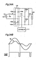
- a power supply device shown in Fig. 34A includes capacitors 120a and 120b for improving a power factor.
- a control circuit 111 outputs a pulse signal for turning on a bi-directional switch 115 for a predetermined time in the vicinity of the zero cross point of the AC power supply 101.
- a charging current flows to the capacitor 120a or 120b via a reactor 102 and a rectifier circuit 103.
- a phase of the charging current is advanced, it is therefore possible to make early a rise of the input current
- the bi-directional switch 115 becomes off, an input current flows through the reactor 102, the rectifier circuit 103 and a smoothing circuit 104. Consequently, a conduction period of the input current can be widened to improve a power factor.
- the control circuit 111 can change an output voltage value by changing a pulse width of the pulse signal. More specifically, the power supply device shown in Fig. 34A is operated as a full-wave rectifier circuit when the bi-directional switch is off, and is operated as a voltage doubler rectifier circuit when the bi-directional switch is in an on state.
- the control circuit 111 can change an output voltage within a range which is more than a voltage obtained by a full-wave rectification, and is lower than a voltage obtained by a voltage doubler rectification.
- the power supply device shown in Fig. 32A can form the input current into a shape of sine wave and control a power factor to approximately 1, the power supply device has the following problem. More specifically, the control becomes complicate, and a loss in the switching element 107 is increased due to high frequency switching accompanying with waveform shaping, and further, a switching noise increases. Therefore a powerful filter circuit is required for restricting the aforesaid loss. This causes a cost increase, an increase of loss in the filter circuit, and finally efficiency deterioration as a whole.
- the above power supply device shown in Fig. 33A has the following problems although it can remarkably simplify a switching control. More specifically, in particular, a current waveform becomes a non-continuous state as shown in Fig. 33B in a low load, or is too advanced; for this reason, a sufficient power factor can not obtained. Further, an output timing of the pulse signal is delayed for a predetermined time from the zero cross point of the AC power supply, and thereby, an optimum power factor is obtained in a low load. However, the control becomes complicate, because both of a delay time and a pulse width must be controlled.
- the reactor is made into a large size in inputting 200V, and then, a loss is increased in the large-sized reactor. Further, since a voltage applied to switching means becomes high, a component having a high withstand voltage is required. As a result, the component is made into a large size, and a switching loss becomes great in the switching element 107.
- the present invention has been made in order to solve the aforesaid problem in the prior art. It is, therefore, an object of the present invention to provide a power supply device which can obtain high power factor with a simple construction and control without carrying out high frequency switching, prevent an increase of loss in a filter circuit resulting from an increase of loss in a switching element and an increase of switching noise, and can restrict a harmonic and a loss.
- Another object of the present invention is to provide a power supply device which can obtain high power factor in the whole loads even if a switching control is simplified, and can improve a power factor by a simple control.
- another object of the present invention is to provide a power supply device which can prevent an increase in a size of reactor in an input of 200V, and an increase of loss resulting from the increase of the reactor size, and can prevent a switching element from being made into a large size.
- another object of the present invention is to provide a power supply device which can greatly change an output voltage even if a switching control is simplified, and can obtain a sufficient power factor.
- the present invention provides a power supply device.
- the device comprises a rectifier unit, a reactor, a power factor correction unit, a pulse signal controller and a switching driver.
- the rectifier unit rectifies an output voltage of an AC power supply to convert the voltage into a DC voltage.
- the reactor is connected to the rectifier unit.
- the power factor correction unit inputs an output voltage of the rectifier unit via the reactor.
- the power factor correction unit includes a switching circuit, a capacitor circuit and a reverse-current blocking rectifier element.
- the switching circuit comprises a plurality of switching elements connected in series and turning on or off to change a current path in the power factor correction unit.
- the capacitor circuit comprises a plurality of capacitors connected in series.
- the reverse-current blocking rectifier element prevents the charge in the capacitors from flowing reversely when the switching circuit turns on.
- the switching circuit and the capacitor circuit is arranged in parallel. At lest one of connection nodes between the switching elements is connected to one connection node between the capacitors.
- Ends of the switching circuit is connected to ends of the capacitor circuit via the reverse-current blocking rectifier element.
- the pulse signal controller generates and outputs a pulse signal to turn on and off each switching element of the power factor correction unit.
- the switching driver receives the pulse signal to drive the switching circuit of the power factor correction unit based on the received pulse signal.
- the pulse signal controller may change a control method of the pulse signal in accordance with a zero cross point of the AC supply voltage, magnitude of the AC supply voltage, status of a load, or the frequency of the AC supply voltage. For example, the pulse signal controller may select one control method from a plurality of methods for controlling the pulse signal in accordance with status of a load
- the power supply device In the power supply device according to the present invention, a wide conduction period can be obtained to restrict a harmonic distortion, and realize a power supply device which can reduce a switching noise and a loss by a simple construction and control. Further the power supply device according to the present invention provides a low-loss air conditioner which has high power factor and can restrict a harmonic distortion.
- An air conditioner with high efficiency, low harmonic and low loss also can be provided by applying thereto the power supply device according to the present invention.
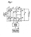
- Fig. 1 is a circuit diagram showing a construction of a power supply device according to one embodiment of the present invention.
- the power supply device comprises a rectifier circuit 2 for rectifying an AC voltage from an AC power supply 1 to output a rectified ripple voltage, a reactor 3 for improving a power factor, a power factor correction circuit 7 and a smoothing capacitor 8 for smoothing an output voltage of the power factor correction circuit 7 to supply the voltage to a load 9.
- the rectifier circuit 2 is composed of a plurality of rectifier elements 2a, 2b, 2c and 2d.
- the power factor correction circuit 7 is composed of two switching elements 4a and 4b connected in series, and two capacitors 5a and 5b connected in series, and two reverse blocking rectifier elements 6a and 6b.
- An intermediate point of the serial connection of two switching elements 4a and 4b is connected with an intermediate point of the serial connection of two capacitors 5a and 5b.
- the switching element 4a and the capacitor 5a are connected via the reverse blocking rectifier element 6a.
- the switching element 4b and the capacitor 5b are connected via the reverse blocking rectifier element 6b.
- the power supply device includes a pulse signal controller 22 which generates and outputs a pulse signal for driving the switching elements 4a and 4b, and a switch driver 23 which receives a pulse signal from the pulse signal controller 22 to drive the switching elements 4a and 4b.
- the pulse signal controller 22 comprises a general logic circuit or a microprocessor.
- the switch driver 23 comprises a transistor, a dedicated IC or a photo-coupler for electrical insulation.
- the pulse signal controller 22 generates and outputs a pulse signal for turning on at least one of two switching elements 4a and 4b in a half period of AC power supply 1.
- Fig. 2 is a view showing a pulse signal outputted by the pulse signal controller 22, a power supply voltage, and a waveform of an input current in this embodiment.
- Vin shows a voltage of the AC power supply 1
- Iin shows an input current
- Pa shows a pulse signal for driving the switching element 4a
- Pb shows a pulse signal for driving the switching element 4b.
- pulse signals Pa and Pb having the same pulse width are outputted to two switching elements 4a and 4b at the same timing.
- a short-circuit current flows via the rectifier circuit 2, the reactor 3 and the switching elements 4a and 4b, and thereby, it is possible to make wide a conduction period as compared with the conventional power supply device as shown in Fig. 31.
- the power supply device of this first embodiment As described above, in the power supply device of this first embodiment, a more sufficiently high power factor can be obtained with a simple construction and control. Therefore, it is possible to provide a low-loss power supply device which has a small switching noise, and prevents an increase of loss in a filter circuit and switching elements 4a and 4b.
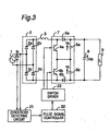
- Fig. 3 is a circuit diagram showing a construction of a power supply device according to another embodiment of the present invention.
- the power supply device further includes a zero cross detecting circuit 21 which detects a zero cross point of the AC power supply 1, and outputs a zero cross detection signal, in addition to the circuit construction shown in Fig. 1.
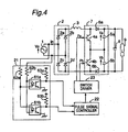
- Fig. 4 shows a construction of the power supply device including the zero cross detecting circuit 21 shown in detail.
- the zero cross detecting circuit 21 alternately detects a zero cross point of the AC power supply 1 for each half period with the use of resistors 62a, 62b, 63a and 63b and photo-couplers 61a and 61b.
- the pulse signal controller 22 receives a zero cross detection signal from the zero cross detecting circuit 21, and then, generates and outputs a pulse signal for driving the switching elements 4a and 4b.
- This pulse signal controller 22 is composed of a general logic circuit or a microprocessor.
- the switch driver 23 receives a pulse signal from the pulse signal controller 22 so as to drive the switching elements 4a and 4b.
- the pulse signal controller 22 generates and outputs two kinds of pulse signals for turning on two switching elements 4a and 4b respectively in a half-period of AC power supply 1.
- the two kinds of pulse signals are alternately switched over for each half period of the AC power supply 1, and then, are outputted to two switching elements 4a and 4b, and thereby, it is possible to uniformly supply a charging current to two capacitors 5a and 5b alternately for each half period, and thus, to widen a conduction period thereby improving a power factor.
- Fig. 5 is a view showing a pulse signal outputted by the pulse signal controller 22, a power supply voltage and a principal waveform of an input current in this second embodiment.
- the pulse signal controller 22 outputs two pulse signals to the switching element 4a and outputs one pulse signal to the switching element 4b in a positive half period of the power supply voltage Vin in synchronous with the zero cross point of the AC power supply 1.
- the umber of pulse signals is switched over, more specifically, the pulse signal controller 22 outputs one pulse signal to the switching element 4a and outputs two pulse signals to the switching element 4b.
- a switch-over of an output pattern of the pulse signal is carried out for each half period of the AC power supply 1.
- the pulse signals Pa and Pb outputted to two switching elements 4a and 4b are switched over for each half period of the AC power supply 1.
- a short-circuit current via the reactor 3 which has a relatively sudden current increase
- a charging current to the capacitor 5a or 5b which has a relatively gentle current increase. Therefore, by use of these currents, and by change of circuit constant in combination with the use of these currents, it is possible to obtain various current waveforms to achieve a higher power factor.
- a low-loss power supply device which can generate small noise and restrict an increase of loss in a filter circuit and the switching elements 4a and 4b can be provided.
- This second embodiment has described an output pattern such that two or one pulse signal is alternately outputted to two switching elements 4a and 4b for each half period.
- the output pattern is not limited to this pattern.
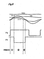
- Fig. 6 is a view showing each waveform (hereinafter, referred to as "principal waveform) of a power supply voltage, an input current and both ends voltage of each capacitor, and a waveform of a pulse in a power supply device according to still another embodiment of the present invention.
- Fig. 7 is a view showing a change of a current flowing path in the power supply device. A positive half period of a power supply voltage is divided into five periods, and then, an operation of each period will be described below in detail with reference to Figs. 3, 6 and 7. In the following description, “Va” or “Vb” shows a voltage across capacitors 5a or 5b respectively, and “Vdc” shows a voltage across the smoothing capacitor 8.
- the operation from the Period 1 ⁇ to Period 5 ⁇ described above can make early a rise of the input current as compared with the conventional case, and widen a conduction period of the input current.
- the pulse signal controller 22 outputs a pulse signal for turning on the switching element 4b for a predetermined time.
- a voltage to the load side seen from the AC power supply 1 becomes equal to the voltage Va of the capacitor 5a.
- a charging current to the capacitor 5a starts to flow from the point where the power supply voltage Vin becomes larger than the Va along a current flowing path as shown in Fig. 7B. After that, the same operation as the positive half period of the AC power supply 1 is carried out.
- the power supply device of this third embodiment can realize a reduction of a harmonic distortion contained in the input current by a simple construction and by a very simple control of one-time pulse signal output in the half period of the power supply voltage. This allows a low-loss power supply device to have a small switching noise, and restrict an increase of loss in a filter circuit and the switching elements 4a and 4b.
- the power supply device of this embodiment is effective specially in case where the power supply device of this embodiment is applied to equipment such as an air conditioner or the like, and in case where the AC power supply 1 is 200V, when the switching element 4a or 4b is in an on state, a voltage applied to the reactor 3 is moderated only by the voltages Va and Vb of the capacitors 5a and 5b. Therefore, it is possible to greatly make the reactor 3 into a small size as compared with the conventional power supply device shown in Fig. 33. Thus, the system can be miniaturized as a whole and reduce a loss in the reactor 3 to achieve a low loss of equipment.
- Fig. 8 is a view showing a pulse signal and a waveform of a principal waveform in a power supply device according to still another embodiment of the present invention.
- a positive half period of a power supply voltage is divided into three periods, and then, an operation of each period will be described below in detail with reference to Fig. 3, Fig. 7 and Fig. 8.
- the operation from the Period 1 ⁇ to the Period 3 ⁇ can make early a rise of the input current as compared with the conventional power supply device to widen a conduction period of the input current.
- the pulse signal controller 22 detects the zero cross point, and thereafter, conversely to the case of the positive half period of the AC power supply 1, outputs a pulse signal Pa for turning on the switching element 4a for a relatively short time, and a pulse signal Pb for turning on the switching element 4b for a time which is longer than that of the switching element 4a and is equal to or shorter than a half period of the AC power supply 1.
- the same operation as the positive half period is performed to make early a rise of the input current as compared with the conventional power supply device and to obtain a current waveform having a wide conduction period.
- the power supply device of this fourth embodiment in the Period 1 ⁇ , an energy is stored in the reactor 3 by a short-circuit current via the reactor 3 along the current flowing path shown in Fig. 7D.
- the Period 2 ⁇ energy is stored in the capacitors 5a and 5b by the charging current to the capacitor 5b or 5a along the current flowing path shown in Fig. 7A or 7B. Therefore, the power supply device of this embodiment can provide high power factor and the output voltage Vdc sufficiently larger than the voltage Vin of the AC power supply 1.
- an output voltage higher than a voltage obtained by voltage doubler rectification can be provided.
- the power supply device of this embodiment can enlarge a conduction period by a very simple control of one-time pulse signal output by output of a pulse signal having different pulse in the half period of the power supply voltage to two switching elements 4a and 4b respectively.
- a sufficiently high power factor can be achieved.
- a switching noise is small, and it is possible to restrict an increase of loss in a filter circuit and the switching elements 4a and 4b. Therefore, a reduction of loss can be achieved.
- an output voltage is increased greater than a voltage obtained by voltage doubler rectification, it is possible to provide a power supply device which is adaptable to a load requiring a high DC voltage.
- a pulse width of two pulse signals Pa and Pb having different pulse width is controlled within a range less than the half period of the power supply voltage. Therefore, it is possible to control an output voltage value of the power supply device in a wide range while obtaining high power factor correction effect.
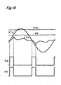
- Fig. 10 is a view showing a pulse signal and a waveform of a principal waveform in a power supply device according to still another embodiment of the present invention.
- the fifth embodiment will be described below in detail with reference to Figs. 3, 7 and 10.
- pulse signals Pa and Pb having the same pulse width are simultaneously outputted to both two switching elements 4a and 4b in synchronous with a zero cross detection signal from the zero cross detecting circuit 21.
- a short-circuit current flows via the rectifier circuit 2, the reactor 3 and the switching elements 4a and 4b along the current flowing path shown in Fig. 7D. Therefore, the input current lin can flow in the vicinity of the zero cross point of the AC power supply 1 where there is primitively no current flow.
- the input current lin can rise up in synchronous with the zero cross point it is possible to greatly widen a conduction period so as to obtain a sufficiently high power factor, and to reduce a harmonic distortion contained in the input current Iin.
- the conduction period is enlarged by a simple control of simultaneously turning on two switching elements 4a and 4b in a half period of the power supply voltage. Therefore, a sufficiently high power factor can be obtained to greatly reduce a harmonic distortion contained in the input current.
- a switching noise becomes small, and it is possible to restrict an increase of loss in a filter circuit and the switching elements 4a and 4b so as to achieve a low loss. Therefore, an energy can be stored in the reactor 3 by a short-circuit current via the reactor 3 to increase an output voltage Vdc.
- a voltage applied to each of the switching elements 4a and 4b is a half of the conventional case shown in Fig. 33. Therefore, a switching loss in the switching elements 4a and 4b can be reduced.
- the input current is small, that is, in a low load, it is possible to realize a low-loss power supply device.
- the above effect is not limited to this fifth embodiment, and the same effect can be obtained in the power supply device of other embodiments.
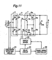
- Fig. 11 is a circuit diagram showing a construction of a power supply device according to still another embodiment of the present invention.
- the power supply device further includes a detection signal delay circuit 24 in addition to the circuit structure shown in Fig. 3.
- the detection signal delay circuit 24 receives a zero cross detection signal from the zero cross detecting circuit 21, delays the received signal by only predetermined time to generate a zero cross delay signal, and outputs the delay signal to the pulse signal controller 22.
- the detection signal delay section 24 comprises a delay circuit including a capacitance and a resistance and using a charging time constant, an IC having a timer function, a microprocessor or the like.
- the pulse signal control signal 22 receives a zero cross delay signal delayed for a predetermined time from the zero cross point obtained by the detection signal delay section 24, and then, outputs a pulse signal for turning on at least one of the switching elements 4a and 4b for a predetermined time.
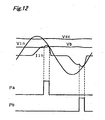
- Fig. 12 is a view showing a pulse signal and a principal waveform in the power supply device of this sixth embodiment.
- the switching element 4a in the positive half period of the AC power supply 1, the switching element 4a is turned on in a portion of a latter-half phase of the half period by the pulse signal Pa, and in the negative half period of the AC power supply 1, the switching element 4b is turned on in a portion of a latter-half phase of the half period by the pulse signal Pb.
- the pulse signal is delayed, and thereby, in the latter-half phase portion of the input current, the pulse signal is outputted at the same timing as in the former half phase for each half period of the power supply voltage. Therefore, a charging current flows to the capacitors 5a and 5b so as to widen a conduction period.
- the power supply device of this sixth embodiment by delaying the pulse signal from the zero cross point of the AC power supply 1 for a predetermined time, the input current can flow in an arbitrary phase interval of the half period. Therefore, the power supply device has the following advantages in particular.
- the pulse signal which is outputted in a period where no current primitively flows can greatly enlarge a conduction period to obtain high power factor.
- a noise is lowered, and a filter circuit is simplified, and further, a loss in the switching means is lowed. Therefore, it is possible to provide a low-loss power supply device which has a simple construction.
- by combining the pulse signal control in the above embodiment can widen a conduction period. Thus, a power factor can be greatly improved and also a harmonic distortion can be restricted.
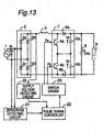
- Fig. 13 is a circuit diagram showing a construction of a power supply device according to still another embodiment of the present invention.
- the power supply device further includes a supply voltage detecting circuit 25 for detecting a voltage of the AC power supply 1, in addition to the circuit construction shown in Fig. 3.
- the supply voltage detecting circuit 25 is composed using a resistor, a transformer on requiring insulation or the like, and detects an alternating voltage Vin or an output ripple voltage
- the pulse signal controller 22 receives a value of the power supply voltage obtained from the supply voltage detecting circuit 25, and then, outputs a pulse signal for turning on at least one of the switching elements 4a and 4b for a predetermined time in synchronous with the time when the power supply voltage value reaches a predetermined value.
- the pulse signal is outputted at the same timing every time for each half period of the AC power supply 1, so that a conduction period can be accurately enlarged for each period of the AC power supply 1. Therefore, it is possible to obtain high power factor, and to accurately restrict a harmonic distortion. Whereby a power supply device having a high reliability can be obtained.
- a control for outputting a pulse signal is carried out on the basis of the voltage value of the power supply 1 obtained from the supply voltage detecting circuit 25 which reaches a predetermined value.
- an output voltage Vdc increases and decreases in accordance with an increase and decrease of the voltage value.
- an output timing of the pulse signal automatically changes when the power supply voltage varies.
- the switching elements 4a and 4b become an on state when the power supply voltage is smaller than usual.
- an energy stored in the reactor 3 or the capacitors 5a and 5b decreases and the output voltage Vdc decreases.
- the switching elements 4a and 4b become an on state when the power supply voltage is larger than usual.
- the output voltage Vdc increases. Therefore, in the power supply device of this seventh embodiment in the case where a variation of power supply voltage is small, an output voltage can be kept substantially constant, and the power supply device has an advantage of being durable to a disturbance.
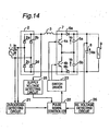
- Fig. 14 is a circuit diagram showing a construction of a power supply device according to still another embodiment of the present invention.
- the power supply device further includes a DC voltage detecting circuit 26 for detecting a voltage Vdc of the smoothing capacitor 8, in addition to the circuit construction shown in Fig. 13.
- the DC voltage detecting circuit 26 is composed of a resistor or the like. An output of the DC voltage detecting circuit 26 is captured in a microprocessor with the use of an A/D converter or the like.
- the DC voltage detecting circuit 26 may detect an output voltage of the power supply device or an output voltage of the power factor correction circuit 7.
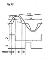
- Fig. 15 is a view showing a pulse signal and a principal waveform in the power supply device of this eighth embodiment.
- a positive half period of the power supply voltage is divided into four (4) periods, and an operation of each period will be described below with reference to Figs. 7, 14 and 15.
- the operation from the Period 1 ⁇ to the Period4 ⁇ can make early a rise of the input current Iin as compared with the conventional case, Therefore, a current waveform having a wide conduction period can be obtained, and also, in a switch-over point of the Period 2 ⁇ and the Period 3 ⁇ , a smoother current waveform can be obtained without forming a sharp current waveform as shown in Fig. 6 of the third embodiment.
- the pulse signal controller 22 outputs a pulse signal Pb for turning on the switching elements 4b until the voltage value Vin of the AC power supply 1 becomes a value more than the voltage Vdc of the smoothing capacitor 8.
- the same operation as the positive half period is carried out, and thereby, a conduction period becomes wide, and it is possible to obtain a smoother current waveform having no sharpness.
- the power supply device of this eighth embodiment it is possible to enlarge a conduction period of input current by a very simple control of outputting one-time pulse signal in the half period of the power supply voltage. Further, it is possible to optimize the timing of switching over the pulse signal from an on state to an off state, so that a sharpness of current waveform can be eliminated. As a result, a smoother current waveform can be obtained, and also, a harmonic distortion contained in the input current can be greatly reduced.
- the power supply device generates a low noise, and it is possible to simplify a filter circuit, and further, switching is one time in a half period of the AC power supply 1. Therefore, a loss of the switching elements 4a and 4b can be reduced, and a low-loss power supply device can be realized.
- the following concept of this eighth embodiment is applicable to the power supply device shown in the first to seventh embodiments. The concept is to detect a voltage of the smoothing capacitor 8, and compare the power supply voltage Vin with the detected voltage Vdc of the smoothing capacitor 8, and thus, to control a timing of the pulse signal.
- Fig. 16 is a circuit diagram showing a construction of a power supply device according to still another embodiment of the present invention.
- the power supply device further includes a DC voltage detecting circuit 26 for detecting a voltage Vdc of the smoothing capacitor 8 and a load status detecting circuit 27 for detecting a magnitude of load, in addition to the circuit construction shown in Fig. 3.
- the load status detecting circuit 27 determines a magnitude of load 9 based on the voltage Vdc of the smoothing capacitor 8 obtained from the DC voltage detecting circuit 26, and a load current obtained by a load current detecting circuit 71 which includes a resistor or a current transformer.
- the pulse signal controller 22 reads each output from the load status detecting circuit 27 and the DC voltage detecting circuit 26, and then, generates and outputs a pulse signal for driving the switching elements 4a and 4b.
- the pulse signal controller 22 changes a pulse width of a pulse signal for turning on the switching elements 4a and 4b, in accordance with a magnitude of load obtained from the load status detecting circuit 27.
- the pulse width may be changed in proportional to a magnitude of load obtained from the load status detecting circuit 27.
- a pulse width capable of maximizing a power factor or efficiency is preset based on a magnitude of a predetermined load. Then, a pulse signal having the preset predetermined pulse width may be outputted in accordance with a magnitude of the detected load.
- a pulse width is preset so that an output voltage is set to a predetermined value in accordance with a magnitude of load, and then, a pulse signal having the preset predetermined pulse width may be outputted in accordance with a magnitude of the detected load.
- the pulse signal controller 22 detects the voltage Vdc value of the smoothing capacitor 8 from the DC voltage detecting circuit 26, and thereby, it is confirmed whether a predetermined voltage is obtained, so that an output voltage can be more securely controlled.
- the power supply device of this ninth embodiment can be combined with the power supply device shown in the above embodiments, and thereby, the same advantage as the above invention can be obtained in all loads. Therefore, in the power supply device of this embodiment, a pulse width is changed in proportion to a magnitude of load. Thereby, it is possible to simplify a control, and to obtain a sufficiently high power factor in all loads. Thus it is possible to restrict a harmonic wave in all load by a simple control. Moreover, a pulse width capable of maximizing a power factor or efficiency is preset in accordance with a magnitude of a predetermined load, and then, a pulse signal having the preset predetermined pulse width is outputted in accordance with a magnitude of the detected load.
- a harmonic distortion can be greatly reduced.
- the harmonic can be restricted, and a low-loss power supply device can be realized.
- a pulse width is preset so that an output voltage is set to a predetermined value in accordance with a magnitude of load, and then, a pulse signal having the preset predetermined pulse width is outputted in accordance with a magnitude of the detected load, and thereby, it is possible to obtain an arbitrary output voltage in all range of the load.
- a harmonic distortion and to realize high power.
- the load status detecting circuit 27 computes the voltage of the smoothing capacitor 8 obtained from the DC voltage detecting circuit 26, and a magnitude of load from a load current obtained from the load current detecting circuit 71 comprising a resistor or a current transformer.
- a load detecting method is not limited to the above method, and it can determine a load status from an output voltage, an output current, an input current and a current flowing through the switching means, as the detecting method. Further, combination of the aforesaid parameters can be used to detect a load.
- Fig. 17 is a circuit diagram showing a construction of a power supply device according to still another embodiment of the present invention.
- the power supply device shown in Fig. 17 is different from the power supply device of the above ninth embodiment in that the pulse signal controller 22 outputs a pulse signal on the basis of only detection signal from the load status detecting circuit 27.
- the pulse signal controller 22 selects a pulse signal for turning on the switching elements 4a and 4b from any of pulse signal output patterns in the power supply devices shown in the above first to ninth embodiments in accordance with a magnitude of load obtained from the load status detecting circuit 27, and then, outputs it.
- Figs. 18A and 18B are views showing a pulse signal outputted by the pulse signal controller 22 and its principal waveform in the power supply device of this tenth embodiment.
- "Pa1” and “Pa2” show a pulse signal for driving the switching element 4a
- "Pb1” and “ Pb2” show a pulse signal for driving the switching element 4b.
- a pulse signal of the output pattern shown in the third embodiment is outputted.
- a pulse signal of the output pattern shown in the fourth embodiment is outputted.
- the pulse signal controller 22 outputs a pulse signal Pa1 and Pb1 as shown in Fig. 18A. In the case of W ⁇ Y1, the pulse signal controller 22 outputs a pulse signal Pa2 and Pb2 as shown in Fig. 18B.
- widening a pulse width in proportion to the magnitude W of load can gradually change the output voltage from a voltage obtained by full wave rectification to a voltage value larger than a voltage obtained by voltage doubler rectification.
- an another predetermined value Y2 may be preset, and the pulse signals may be both turned off when the magnitude of load is equal to or less than Y2. More specifically, in the case of W ⁇ Y2, the pulse signal controller 22 outputs no pulse signal. On the other hand, in the case of Y2 ⁇ W ⁇ Y1, the pulse signal controller 22 outputs the pulse signals Pa1 and Pb1 as shown in Fig. 18A. Further, in the case of W ⁇ Y1, the pulse signal controller 22 outputs the pulse signals Pa2 and Pb2 as shown in Fig. 18B.
- the magnitude W of load is compared with a predetermined value, and a pulse signal to be outputted is changed in accordance with the magnitude of the load.
- a pulse signal to be outputted is changed in accordance with the magnitude of the load.
- the circuit construction and control of the power supply device are simplified. Therefore, a switching noise becomes small, and a filter circuit is simplified, and further a loss in the switching means becomes small. Thus a low-loss power supply device can be provided.
- Combination of the pulse signal output pattern of the power supply device of this tenth embodiment may be used in the power supply devices shown in the first to ninth embodiments.
- the load status detecting circuit 27 determines a magnitude of load, the voltage of the smoothing capacitor 8 obtained from the DC voltage detecting circuit 26, and a load current obtained from the load current detecting circuit 71.
- a load detecting method is not limited to the above method, for example, it is possible to determine a load from an output voltage, an output current an input current of the power supply device, a current flowing through the switching element, pulse width or the combination thereof to detect the load.
- Fig. 19 is a circuit diagram showing a construction of a power supply device according to still another embodiment of the present invention.
- the power supply device includes an inverter 10 and a load status detecting circuit 27, in addition to the circuit configuration shown in Fig. 3.
- the inverter 10 is composed of a plurality of semiconductor elements, and the semiconductor elements are switched over according to a high frequency. Thereby, a substantially DC voltage Vdc of the both terminals of the smoothing capacitor 8 is converted into an AC voltage of a variable voltage/variable frequency.
- Self arc-extinguishable semiconductors such as a power transistor, a power MOSFET, IGBT are used as the semiconductor element, like the switching elements of the power factor correction circuit 7.
- the AC voltage of variable voltage/variable frequency outputted by the inverter 10 is supplied to a motor 11 so that the motor 11 is driven at a variable speed.
- a DC brushless motor is used as the motor 11.
- the load status detecting circuit 27 is composed of an inverter controller 30, an inverter driver 31 and a position detecting circuit 32.
- the position detecting circuit 32 detects a rotor position of the motor 11, that is, the DC brushless motor, and outputs a positional detection signal.
- the position detecting circuit 32 comprises a Hall sensor, an encoder or the like.
- the inverter controller 30 generates and outputs a control signal for driving the inverter 10 on the basis of the positional detection signal from the position detecting circuit 32, and comprises a microprocessor or the like.
- the inverter driver 31 drives the semiconductor element of the inverter 10 on the basis of the control signal generated and outputted by the inverter controller 30.
- the pulse signal controller 22 generates and outputs a pulse signal for driving the switching elements 4a and 4b, and also, in this eleventh embodiment, reads a load state detected by the inverter controller 30 which is one of components of the load status detecting circuit 27.
- the inverter controller 30 receives an external speed command signal and a positional detection signal from the position detecting circuit 32, and generates a control signal for driving the inverter 10 in order to control the motor to a predetermined speed.
- the motor 11 which is driven at a variable speed by the inverter 10
- a motor for compressor used in an air conditioner.
- a load torque increases in accordance with a magnitude of speed, and a counter electromotive voltage generated in a motor winding increases. Therefore a voltage and a current applied to the motor 11 become large, and an output power increases.
- an input power and an input current by the AC power supply are also increased.
- the pulse signal controller 22 outputs a pulse signal for driving the switching elements 4a and 4b.
- a power factor or efficiency of the power supply device depends greatly on a pulse width of the pulse signal. Therefore, in order to maximize the power factor or efficiency, there is a need of outputting a pulse signal having an optimum pulse width.
- the optimum pulse width differs depending upon a magnitude of load, a circuit constant or the like.
- the following method is used as a method for detecting a magnitude of load.
- a computation is carried out based on a speed of the motor 11 obtained from a detection interval of the positional detection signal outputted by the position detecting circuit 32.
- a pulse width capable of maximizing a power factor or efficiency is preset with respect to a speed of the motor 11. Then, the pulse signal controller 22 may output a pulse signal having a preset predetermined pulse width in accordance with the detected speed of the motor 11. Moreover, when the optimum pulse width is proportional substantially to a speed of the motor 11, as shown in Fig. 20, the pulse signal controller 22 may control a pulse width of the pulse signal in proportion to the detected speed of the motor 11.
- the magnitude of load is computed based on the speed of the motor 11, and a pulse width capable of maximizing a power factor or efficiency is preset with respect to the speed of the motor 11, and further, a predetermined pulse signal is outputted in accordance with the speed of the motor 11. Therefore, it is possible to obtain a sufficient power factor or efficiency in all operating ranges of the motor 11. Whereby it is possible to sufficiently reduce a harmonic distortion contained in an input current in all operating ranges of the motor 11, and to realize a low-loss power supply device for driving a motor.
- a switching noise can be small, and it is possible to restrict an increase of loss in a filter circuit and the switching elements 4a and 4b.
- the pulse width of the pulse signal is controlled in proportion to the detected speed of the motor 11. Therefore, likewise, it is possible to obtain a sufficient power factor or efficiency in all operating ranges of the motor 11.
- the pulse width of the pulse signal is represented as a linear expression to the speed of the motor 11, a pulse width control can be further simplified. Therefore in all operating ranges of the motor 11, it is possible to sufficiently reduce a harmonic distortion contained in an input current by a simple control, and to realize a low-loss power supply device for driving a motor.
- a power supply device according to still another embodiment of the present invention will be described below with reference to Fig. 19, Fig. 21, Fig. 22 and Fig. 23.
- a magnitude of load of the motor 11 is detected on the basis of a magnitude of an input current of the AC power supply 1.
- the magnitude of the input current increases in accordance with the magnitude of load of the motor 11.
- the input current is detected by an input current detecting circuit (not shown) such as a resistor and a current transformer provided on a current flowing path.
- an operation mode by the pulse signal shown in the third embodiment is referred to as “full wave rectification mode”
- an operation mode by the pulse signal shown in the fourth embodiment is referred to as "voltage doubler rectification mode”.
- the pulse signal controller 22 of the power factor correction circuit 7 carries out a power factor correction in the full wave rectification mode.
- a voltage of the AC power supply 1 is 200V
- the voltage Vdc of the smoothing capacitor 8 becomes about 280V.
- the pulse signal controller 22 controls a pulse width of the pulse signal in accordance with a magnitude of the load, that is, a magnitude of the input current so as to maximize a power factor or efficiency. In this interval, in order to control the motor to a predetermined speed on the basis of a speed command signal from the external.
- the inverter controller 30 carries out an inverter PWM (Pulse Width Modulation) control for controlling the motor 11 to a predetermined speed. That is, the inverter controller 30 controls a pulse duty of a high frequency pulse signal for driving each semiconductor element of the inverter 10 to adjust a voltage applied to the motor 11.
- PWM Pulse Width Modulation
- the voltage Vdc of the smoothing capacitor 8 is controlled by a pulse signal control by the power factor correction circuit 7 by the pulse signal controller 22 so that a voltage applied to the motor is adjusted, and thereby, an inverter PAM (Pulse Amplitude Modulation) control for controlling the motor 11 to a predetermined speed is carried out.
- PAM Pulse Amplitude Modulation
- the pulse signal controller 22 of the power factor correction circuit 7 carries out a power factor correction in the full wave rectification mode.
- the voltage Vdc of the smoothing capacitor 8 becomes about 140V.
- the pulse signal controller 22 controls a pulse width of the pulse signal in accordance with a magnitude of the load, that is, a magnitude of the input current to maximize a power factor or efficiency.
- the inverter controller 30 carries out the inverter PWM control for controlling the motor 11 to a predetermined speed on the basis of the speed command signal from the external.
- the pulse duty of the inverter 10 reaches a predetermined value, for example, 100%, a voltage supply to the motor 11 becomes a saturated state, and the speed of the motor is not increased any more.
- a predetermined value for example, 100%
- the voltage Vdc of the smoothing capacitor 8 is controlled according to a pulse signal control by the power factor correction circuit 7 controlled by the pulse signal controller 22 so that a voltage applied to the motor is adjusted, and thereby, the inverter PAM control for controlling the motor 11 to a predetermined speed is carried out.
- the pulse signal controller switches over the pulse signal to be outputted from the full wave rectification mode to the voltage doubler rectification mode, and thereby, a greater voltage boost effect can be obtained.
- the output voltage Vdc is controlled by a pulse width of two pulse signals outputted by two switching elements 4a and 4b of the power factor correction circuit 7.
- a great voltage boost effect in the voltage doubler rectification mode can provide the same output voltage Vdc in input of 100V as output voltage to the input of 200V.
- the inverter PAM control can be performed in a wider range.
- the switch-over from the full wave rectification mode to the voltage doubler rectification mode may not be always carried out at the point at which the pulse duty of the high frequency pulse signal outputted by the inverter controller 30 reaches 100%. As shown in Fig. 23, a switchover of the mode may be after and before the point at which the pulse duty ratio reaches 100%.
- a hysteresis is provided at the switchover point from the full wave rectification mode to the voltage doubler rectification mode.
- the speed of the motor 11 is controlled by the inverter PWM control in a region where a load acting on the motor 11 is small, and is controlled by the inverter PAM control in a region where the load is large. Therefore, a sufficient power factor is obtained in all operating ranges of the motor 11, and in particular, it is possible to restrict a switching loss in an inverter PAM control region. It is therefore possible to realize a low-loss inverter 10 and motor 11. In addition, the output voltage Vdc can be improved.
- a pattern of the pulse signal outputted by the pulse signal controller 22 is not limited to one in this embodiment.
- the output pattern may be selected from the arbitrary combination of patterns of above embodiments as required.
- the motor 11 uses the DC brushless motor.
- the motor used in the power supply device of the present invention is not limited to the DC brushless motor, and the same effect can be obtained in other motors such as an induction motor or the like.
- the load status detecting circuit 27 is not limited to the construction shown in Fig. 19.
- the speed of the motor 11 and a magnitude of the input current of the AC power supply 1 have been used in a method of detecting the load status.
- the parameters such as an output pulse duty of the inverter 10, an output frequency, an output current value, a voltage and current applied to the motor 11, may be used. In addition, combination of these parameters may be used to detect a magnitude of load. The same effect can be obtained.
- the power supply device of this embodiment includes a power supply voltage determining circuit 25', in addition to the circuit construction shown in Fig. 23.
- the pulse signal controller 22 generates and outputs a pulse signal for driving the switching elements 4a and 4b, and in this embodiment, reads a voltage of the AC power supply 1 detected by the power supply voltage determining circuit 25' and a load status detected by the inverter controller 30 which is one component of the load status detecting circuit 27.
- the power supply device shown in Fig. 24 will be described below in detail.
- the power supply voltage determining circuit 25' detects a voltage of the AC power supply 1 from a ripple voltage which is an output of the rectifier circuit 2 and compares the detected voltage with a predetermined value. When the detected voltage value is determined to be 200V by the comparison, a control suitable for the operation with the supply voltage of 200V is carried out. That is, the pulse signal controller 22 controls the pulse signal to improve a power factor in the full wave rectification mode as shown in Fig. 21.
- the inverter controller 30 carries out the inverter PWM control in low and intermediate load regions and carries out the inverter PAM control in a high load region. Thus, a speed of the motor 11 can be controlled.
- the pulse signal controller 22 controls output pulse signal so as to improve a power factor in the full wave rectification mode, and the inverter controller 30 carries out the inverter PWM control.
- the pulse signal controller 22 carries out a power factor correction in the voltage doubler rectification mode, and the inverter controller 30 carries out the inverter PAM control.
- the control method of the power factor correction circuit 7 and inverter 10 is switched in accordance with the voltage of the AC power supply 1 detected by the supply voltage determining circuit 25'. Therefore, it is possible to obtain a sufficient power factor in all operating ranges regardless of the voltage value of the AC power supply 1. In addition, it is possible to reduce a loss, and to improve the output voltage Vdc.
- the voltage value of the AC power supply 1 is 100V or 200V
- a switching noise can be small, and it is possible to restrict an increase of loss in a filter circuit and the switching elements 4a and 4b with a simple control.
- control method shown in Fig. 22 or 23 has been employed in the case where the voltage value of the AC power supply 1 is 100V, and the control method shown in Fig. 21 has been employed when the voltage of the AC power supply 1 is 200V.
- Other control methods however may be combined to be used.
- the power supply device of this embodiment further includes a power-supply frequency detecting circuit 28 for detecting a frequency of the AC power supply 1 to output a frequency detection signal, in addition to the circuit construction shown in Fig. 3.
- the pulse signal controller 22 generates and outputs a pulse signal for driving the switching elements 4a and 4b, and also, reads the frequency detection signal from the power-supply frequency detecting circuit 28.
- the power supply device shown in Fig. 25 will be described below in detail.
- the AC power supply 1 is a commercial power supply
- its frequency is either 50Hz or 60Hz. Time lengths of one period in these frequency are different each other. Therefore, even if a magnitude of the load 9 is the same, an optimum pulse width capable of maximizing a power factor or efficiency is different in each frequency.
- the pulse signal controller 22 In order that the power supply device obtains a sufficient power factor or efficiency regardless of the frequency of the AC power supply 1, the pulse signal controller 22 must output a pulse signal having the optimum pulse width corresponding to each frequency.
- an optimum pulse width capable of maximizing a power factor or efficiency is preset for each frequency of the AC power supply 1.
- the pulse signal controller 22 receives the frequency detection signal of the AC power supply 1 detected by the power-supply frequency detecting circuit 28, and then, outputs the optimum pulse signal in the previously set pulse signals which corresponds to the detected frequency. Or a reference frequency is preset, and an optimum pulse signal corresponding to the reference frequency is preset. Then, in the case where the frequency detected by the power-supply frequency detecting circuit 28 is different from the reference frequency, the pulse signal corresponding to the preset reference frequency is computed based on a predetermined ratio, and thereby, a brief optimum pulse signal is obtained.
- a pulse width capable of optimizing a power factor or efficiency is preset for each frequency of the AC power supply 1, and the pulse signal controller 22 outputs a pulse signal having an optimum pulse width corresponding to each detected frequency. Therefore, it is possible to obtain a sufficient power factor or efficiency regardless of a frequency of the AC power supply 1. Whereby it is possible to sufficiently restrict a harmonic distortion of the input current without performing setting and modification in accordance with a frequency of the AC power supply 1.
- an optimum pulse signal corresponding to a reference frequency is preset and when the detected frequency is different from the reference frequency, the pulse signal controller 22 outputs a pulse signal which is computed with respect to a preset reference pulse signal at a predetermined ratio. Therefore, it is possible to obtain a sufficient power factor or efficiency regardless of a frequency of the AC power supply 1. Whereby it is possible to obtain a sufficient power factor or efficiency regardless of a frequency of the AC power supply 1 without setting pulse signals for all frequencies.
- the optimum pulse signal is preset in accordance with a magnitude of load, but also a pulse width of the pulse signal is varied in proportion to the magnitude of load.
- the power-supply frequency detecting circuit 28 is provided.
- a frequency of the AC power supply 1 however may be computed based on a detection interval of the zero cross detection signal outputted by the zero cross detecting circuit 21. The same advantage can be obtained as one in the other embodiments.
- Fig. 27 shows one example of an air conditioner to which any of the power supply devices of the present invention is applied.
- the air conditioner uses the power supply device shown in the first embodiment as a converter.
- the air conditioner includes an inverter 81, a power-driven compressor 82 and a refrigeration cycle.
- the refrigeration cycle comprises an indoor unit 92, an outdoor unit 95 and a four-way valve 91.
- the indoor unit 92 comprises an indoor heat exchanger 93 and an indoor fan 94.
- the outdoor unit 95 comprises an outdoor heat exchanger 96, an outdoor fan 97 and an expansion valve 98.
- a refrigerant which carries a heat circulates through the refrigeration cycle.
- the refrigerant is compressed by the power-driven compressor 82, and then makes a heat exchange with an outdoor air supplied from the outdoor fan 97 by the outdoor heat exchanger 96, and further, makes a heat exchange with an indoor air supplied from the indoor fan 94 by the indoor heat exchanger 93.
- Room cooling or heating is performed by an air after heat exchange by the indoor heat exchanger 93.
- a switchover of cooling or heating is carried out by inverting a circulating direction of the refrigerant by the four-way valve 91.
- the circulation of refrigerant in the refrigeration cycle is performed by driving the compressor 82 by the inverter 81, and a supply of power to those inverter 81 and the compressor 82 is carried out using the power supply device of the first embodiment which functions as a converter.
- the construction and operation of the power supply device are as described before.
- the power supply device of the first embodiment has been used as a converter. Even in the case where other power supply devices of the second to fourteenth embodiments are used, it is possible to provide an air conditioner having an effect of each power supply device.
- the power supply device of the present invention even if the AC power supply 1 provides 200V, as shown in the third embodiment, a harmonic distortion can be restricted, and a small-size reactor 3 can be realized. Therefore, it is possible to use the same reactor 3 as that used in the input of 100V.
- the fourth embodiment even if the AC power supply 1 is 100V, it is possible to obtain an output voltage higher than a voltage obtained by the voltage doubler rectification in addition to the restriction of harmonic. Therefore, even in the case of the input of 100V, it is possible to obtain the same output voltage as the input of 200V without providing the voltage doubler rectifier circuit. Further, as shown in the ninth to twelfth embodiments, a pulse width and the control method of pulse signal are modified in accordance with a magnitude of load. Therefore, it is possible to obtain an optimum output voltage, power factor and efficiency in all load ranges.
- the power supply device of this embodiment is applicable to any of 100V type and 200V type air conditioners and can restrict a harmonic distortion contained in an input current by the high power factor. Further, the power supply device has the following advantages. More specifically, the circuit construction and components can be used in common, and the number of processes and components can be greatly reduced.
- Fig. 29 shows a current flowing path in the circuit construction shown in Fig. 28.
- the reactor 3 has been connected to a ripple output side of the rectifier circuit 2. As shown in Fig. 30, even in the case where the reactor 3 is connected to an AC input side of the rectifier circuit 2, the same advantages can be obtained.
Landscapes
- Engineering & Computer Science (AREA)
- Power Engineering (AREA)
- Rectifiers (AREA)
Applications Claiming Priority (2)
| Application Number | Priority Date | Filing Date | Title |
|---|---|---|---|
| JP1015599 | 1999-01-19 | ||
| JP1015599 | 1999-01-19 |
Publications (2)
| Publication Number | Publication Date |
|---|---|
| EP1022844A2 true EP1022844A2 (de) | 2000-07-26 |
| EP1022844A3 EP1022844A3 (de) | 2002-04-17 |
Family
ID=11742398
Family Applications (1)
| Application Number | Title | Priority Date | Filing Date |
|---|---|---|---|
| EP00300333A Withdrawn EP1022844A3 (de) | 1999-01-19 | 2000-01-18 | Stromversorgungsvorrichtung und dieselbe benutzende Klimaanlage |
Country Status (4)
| Country | Link |
|---|---|
| US (2) | US6181583B1 (de) |
| EP (1) | EP1022844A3 (de) |
| CN (1) | CN1183654C (de) |
| MY (1) | MY130199A (de) |
Cited By (14)
| Publication number | Priority date | Publication date | Assignee | Title |
|---|---|---|---|---|
| EP1298782A3 (de) * | 2001-09-28 | 2005-04-27 | Matsushita Electric Industrial Co., Ltd. | Wechselrichteranordnung für eine Klimaanlage |
| US7075268B2 (en) | 2004-02-27 | 2006-07-11 | York International Corporation | System and method for increasing output horsepower and efficiency in a motor |
| US7096681B2 (en) | 2004-02-27 | 2006-08-29 | York International Corporation | System and method for variable speed operation of a screw compressor |
| EP1355411A4 (de) * | 2001-01-26 | 2006-12-20 | Matsushita Electric Industrial Co Ltd | Energievorrichtung |
| US7164242B2 (en) | 2004-02-27 | 2007-01-16 | York International Corp. | Variable speed drive for multiple loads |
| US7193826B2 (en) | 2004-02-27 | 2007-03-20 | York International Corporation | Motor disconnect arrangement for a variable speed drive |
| EP1643626A3 (de) * | 2004-09-22 | 2008-01-23 | Matsushita Electric Industrial Co., Ltd. | Gleichstromversorgungsgerät und Regelungsverfahren für dasselbe, und ein Kompressorantriebsgerät |
| EP1598925A3 (de) * | 2004-05-21 | 2008-02-20 | Lg Electronics Inc. | Vorrichtung zur Steuerung der Leistungsfaktorkompensation in Wechselrichtersteuerschaltung und Verfahren dafür |
| EP1835607A3 (de) * | 2006-03-14 | 2008-12-17 | LG Electronics Inc. | Verfahren und Vorrichtung zur Gleichstromversorgung |
| EP1432109A4 (de) * | 2001-09-28 | 2012-04-04 | Panasonic Corp | Stromquellenvorrichtung |
| WO2019088678A1 (en) | 2017-11-02 | 2019-05-09 | Samsung Electronics Co., Ltd. | Air conditioner and rectifier |
| CN109936202A (zh) * | 2017-12-18 | 2019-06-25 | 奥克斯空调股份有限公司 | 一种空调充电电路、充电控制方法以及具有该电路的空调 |
| EP3676945A4 (de) * | 2017-11-02 | 2020-11-04 | Samsung Electronics Co., Ltd. | Klimaanlage und gleichrichter |
| CN113932396A (zh) * | 2020-07-13 | 2022-01-14 | 海信(山东)空调有限公司 | 一种空调器和控制方法 |
Families Citing this family (82)
| Publication number | Priority date | Publication date | Assignee | Title |
|---|---|---|---|---|
| USRE33929E (en) * | 1982-05-28 | 1992-05-19 | Kwik Products International Corporation | Central injection device for internal combustion engines |
| US6882552B2 (en) * | 2000-06-02 | 2005-04-19 | Iwatt, Inc. | Power converter driven by power pulse and sense pulse |
| US6894911B2 (en) * | 2000-06-02 | 2005-05-17 | Iwatt, Inc. | Method of driving a power converter by using a power pulse and a sense pulse |
| US6304473B1 (en) * | 2000-06-02 | 2001-10-16 | Iwatt | Operating a power converter at optimal efficiency |
| US6549438B2 (en) | 2001-04-30 | 2003-04-15 | Precision Automation, Inc. | AC-to-DC converter circuit utilizing IGBT's for improved efficiency |
| JP3846336B2 (ja) * | 2001-06-07 | 2006-11-15 | 株式会社デンソー | 車両用交流発電機の異常検出装置 |
| US6969959B2 (en) * | 2001-07-06 | 2005-11-29 | Lutron Electronics Co., Inc. | Electronic control systems and methods |
| US6862198B2 (en) * | 2001-11-29 | 2005-03-01 | Iwatt, Inc. | PWM power converter with digital sampling control circuitry |
| JP2003176788A (ja) * | 2001-12-10 | 2003-06-27 | Matsushita Electric Ind Co Ltd | リニアコンプレッサの駆動装置 |
| US6834002B2 (en) * | 2003-01-31 | 2004-12-21 | Entrust Power Co., Ltd. | Power factor correction circuit |
| JP2004364491A (ja) * | 2003-05-09 | 2004-12-24 | Sanyo Electric Co Ltd | 電源システム及び空気調和装置 |
| JP4596866B2 (ja) * | 2003-09-09 | 2010-12-15 | パナソニック株式会社 | モータ駆動装置 |
| KR100614330B1 (ko) * | 2004-02-24 | 2006-08-18 | 엘지전자 주식회사 | 인버터 제어회로의 역률개선방법 |
| JP4428140B2 (ja) * | 2004-05-21 | 2010-03-10 | 株式会社デンソー | 電子制御装置,電動パワーステアリング装置,および伝達比可変操舵装置 |
| JP2006223008A (ja) * | 2005-02-08 | 2006-08-24 | Hitachi Ltd | Dc−dcコンバータ |
| CN1987258B (zh) * | 2005-12-23 | 2010-08-25 | 乐金电子(天津)电器有限公司 | 变频空调器以及变频空调器的功率因数补偿方法 |
| US7586764B2 (en) * | 2006-12-13 | 2009-09-08 | Super Micro Computer Inc. | Synchronized rectifier filter control device for protecting a power supply from reverse current |
| US9349528B2 (en) * | 2007-06-01 | 2016-05-24 | Landis+Gyr, Inc. | Power supply arrangement having a boost circuit for an electricity meter |
| CN103647462B (zh) * | 2007-08-29 | 2017-04-26 | 三菱电机株式会社 | 交流直流变换装置、使用该交流直流变换装置的压缩机驱动装置和空调机 |
| US20090085572A1 (en) * | 2007-09-28 | 2009-04-02 | Mcguire Jeffrey D | Method and apparatus for diagnosing inverter linkages |
| US8459053B2 (en) | 2007-10-08 | 2013-06-11 | Emerson Climate Technologies, Inc. | Variable speed compressor protection system and method |
| US20090092502A1 (en) * | 2007-10-08 | 2009-04-09 | Emerson Climate Technologies, Inc. | Compressor having a power factor correction system and method |
| US8731732B2 (en) * | 2008-02-25 | 2014-05-20 | Stanley Klein | Methods and system to manage variability in production of renewable energy |
| DE102008002525A1 (de) * | 2008-06-19 | 2009-12-24 | Robert Bosch Gmbh | Gleichspannungswandler |
| ES2749875T3 (es) * | 2008-08-01 | 2020-03-24 | Mitsubishi Electric Corp | Convertidor de CA-CC, método de control del convertidor de CA-CC, dispositivo de excitación de motor, dispositivo de excitación de compresor, acondicionador de aire y dispositivo de suministro de agua caliente de tipo bomba de calor |
| CN102379081B (zh) * | 2009-04-01 | 2014-03-05 | 三菱电机株式会社 | 电力变换装置 |
| JP5575423B2 (ja) * | 2009-05-25 | 2014-08-20 | 株式会社東芝 | 洗濯機のモータ駆動装置 |
| EP2330729B1 (de) * | 2009-05-27 | 2018-02-07 | Panasonic Intellectual Property Management Co., Ltd. | Umrichtersteuerungsvorrichtung und umrichtersteuerungsverfahren |
| US8094472B2 (en) * | 2009-06-02 | 2012-01-10 | Rhymebus Corporation | Power factor correction converter capable of fast adjusting load |
| US8339090B2 (en) * | 2009-09-08 | 2012-12-25 | Sequence Controls Inc. | Current control apparatus operable in wet environment |
| US8492928B2 (en) * | 2010-03-18 | 2013-07-23 | American Power Conversion Corporation | AC-to-DC conversion |
| GB201006398D0 (en) | 2010-04-16 | 2010-06-02 | Dyson Technology Ltd | Control of a brushless motor |
| GB201006391D0 (en) * | 2010-04-16 | 2010-06-02 | Dyson Technology Ltd | Control of a brushless permanent-magnet motor |
| GB201006396D0 (en) * | 2010-04-16 | 2010-06-02 | Dyson Technology Ltd | Control of a brushless motor |
| GB201006392D0 (en) | 2010-04-16 | 2010-06-02 | Dyson Technology Ltd | Controller for a brushless motor |
| GB201006386D0 (en) * | 2010-04-16 | 2010-06-02 | Dyson Technology Ltd | Control of a brushless motor |
| GB201006388D0 (en) | 2010-04-16 | 2010-06-02 | Dyson Technology Ltd | Control of brushless motor |
| GB201006395D0 (en) | 2010-04-16 | 2010-06-02 | Dyson Technology Ltd | Control of a brushless motor |
| GB201006397D0 (en) | 2010-04-16 | 2010-06-02 | Dyson Technology Ltd | Control of a brushless motor |
| GB201006390D0 (en) * | 2010-04-16 | 2010-06-02 | Dyson Technology Ltd | Control of a brushless motor |
| GB201006387D0 (en) | 2010-04-16 | 2010-06-02 | Dyson Technology Ltd | Control of a brushless motor |
| JP2012019637A (ja) * | 2010-07-08 | 2012-01-26 | Fujitsu Ltd | 分圧力率改善回路、分圧力率改善装置および分圧力率改善方法 |
| JP5007764B2 (ja) * | 2010-09-22 | 2012-08-22 | ダイキン工業株式会社 | モータ駆動システム及びモータシステム |
| GB2484289B (en) | 2010-10-04 | 2013-11-20 | Dyson Technology Ltd | Control of an electrical machine |
| US9948203B2 (en) * | 2011-10-28 | 2018-04-17 | Mitsubishi Electric Corporation | Direct-current power supply device and electric motor driving device |
| CN102447403B (zh) * | 2011-11-09 | 2014-02-26 | 北京工业大学 | 一种低谐波连续输入电流的三相整流电路 |
| JP5966606B2 (ja) * | 2012-05-17 | 2016-08-10 | 富士電機株式会社 | スイッチング電源装置 |
| US10112251B2 (en) | 2012-07-23 | 2018-10-30 | Illinois Tool Works Inc. | Method and apparatus for providing welding type power |
| US11161193B2 (en) | 2012-07-23 | 2021-11-02 | Illinois Tool Works Inc. | Method and apparatus for providing welding type power with flux balancing |
| TWI489124B (zh) * | 2012-07-26 | 2015-06-21 | Delta Electronics Inc | 電力資訊的獲取方法 |
| CN104704733B (zh) * | 2012-10-10 | 2017-05-03 | 大金工业株式会社 | 直接型电力转换装置以及直接型电力转换装置的控制方法 |
| JP6028653B2 (ja) * | 2013-03-27 | 2016-11-16 | ブラザー工業株式会社 | 電源システム、同電源システムを備えた画像形成装置 |
| JP5974952B2 (ja) * | 2013-03-27 | 2016-08-23 | ブラザー工業株式会社 | 電源システム、同電源システムを備えた画像形成装置 |
| WO2014207824A1 (ja) | 2013-06-25 | 2014-12-31 | 三菱電機株式会社 | 直流電源装置、およびそれを備えた冷凍サイクル適用機器 |
| WO2015033437A1 (ja) | 2013-09-06 | 2015-03-12 | 三菱電機株式会社 | 直流電源装置、およびそれを備えた冷凍サイクル適用機器 |
| WO2015056341A1 (ja) * | 2013-10-18 | 2015-04-23 | 三菱電機株式会社 | 直流電源装置、電動機駆動装置、空気調和機および冷蔵庫 |
| MX353700B (es) * | 2013-10-18 | 2018-01-25 | Mitsubishi Electric Corp | Dispositivo de suministro de energía de corriente directa, dispositivo de accionamiento de motor, aire acondicionado y refrigerador. |
| WO2015063869A1 (ja) | 2013-10-29 | 2015-05-07 | 三菱電機株式会社 | 直流電源装置及び冷凍サイクル機器 |
| WO2015079504A1 (ja) * | 2013-11-26 | 2015-06-04 | 三菱電機株式会社 | 直流電源装置、およびそれを備えた冷凍サイクル適用機器 |
| JP6336031B2 (ja) | 2014-02-19 | 2018-06-06 | 三菱電機株式会社 | 直流電源装置および、それを備えた電動機駆動装置、ならびに、それを備えた冷凍サイクル適用機器 |
| EP2911298A1 (de) * | 2014-02-25 | 2015-08-26 | ABB Oy | Gate-Treiberschaltung mit einem Spannungsstabilisator und einem Verfahren |
| CN106416040B (zh) * | 2014-06-05 | 2019-06-25 | 三菱电机株式会社 | 直流电源装置和具备该直流电源的制冷循环应用设备 |
| US9941834B2 (en) * | 2014-07-03 | 2018-04-10 | Mitsubishi Electric Corporation | Power conversion apparatus and air-conditioning apparatus including the power conversion apparatus |
| WO2016006045A1 (ja) * | 2014-07-08 | 2016-01-14 | 三菱電機株式会社 | 電力変換装置 |
| KR101720915B1 (ko) * | 2015-01-19 | 2017-03-28 | 미쓰비시덴키 가부시키가이샤 | 회생 컨버터 |
| US9806601B2 (en) * | 2015-03-27 | 2017-10-31 | Futurewei Technologies, Inc. | Boost converter and method |
| US20180145616A1 (en) * | 2015-05-29 | 2018-05-24 | Nidec Corporation | Dc-brushless-motor control device |
| JP6128201B1 (ja) * | 2015-12-28 | 2017-05-17 | ダイキン工業株式会社 | 電源装置、その電源装置を用いたインバータ装置、並びにコンバータ装置、及びそのインバータ装置又はコンバータ装置を用いた冷凍装置、並びに空気清浄器 |
| JP6522228B2 (ja) | 2016-02-25 | 2019-05-29 | 三菱電機株式会社 | 直流電源装置および冷凍サイクル適用機器 |
| CN106533152B (zh) * | 2016-12-07 | 2019-01-18 | 南京理工大学 | 一种提高Boost三电平变换器PF的装置及方法 |
| CN107462856B (zh) * | 2017-08-09 | 2019-10-08 | 科华恒盛股份有限公司 | 一种交流电检测单元失效的判断方法 |
| WO2019056192A1 (zh) * | 2017-09-19 | 2019-03-28 | 深圳市汇顶科技股份有限公司 | 上电复位时间的测量方法及系统 |
| CN108363318A (zh) * | 2018-02-11 | 2018-08-03 | 四川虹美智能科技有限公司 | 一种控制开关状态切换的方法、系统及一种控制芯片 |
| US10396652B1 (en) | 2018-04-27 | 2019-08-27 | Hewlett Packard Enterprise Development Lp | Controlled power adjustments |
| CN108709294B (zh) * | 2018-07-18 | 2024-05-10 | 珠海格力电器股份有限公司 | 供电电路、电器的控制器及其控制方法、空调 |
| WO2020066033A1 (ja) * | 2018-09-28 | 2020-04-02 | 三菱電機株式会社 | 電力変換装置、モータ駆動装置及び空気調和機 |
| JP2020096463A (ja) * | 2018-12-13 | 2020-06-18 | 日本電産サーボ株式会社 | 制御装置、及びモータ |
| JP6987301B2 (ja) * | 2019-04-12 | 2021-12-22 | 三菱電機株式会社 | 直流電源装置および空気調和機 |
| US11206743B2 (en) | 2019-07-25 | 2021-12-21 | Emerson Climate Technolgies, Inc. | Electronics enclosure with heat-transfer element |
| CN112436760A (zh) * | 2019-08-23 | 2021-03-02 | 广东美的生活电器制造有限公司 | 电机的控制装置、方法、系统、家用电器及存储介质 |
| CN112886808B (zh) * | 2019-11-29 | 2022-06-10 | 广东美的制冷设备有限公司 | 控制方法、装置、家电设备和计算机可读存储介质 |
| JP2022125765A (ja) * | 2021-02-17 | 2022-08-29 | キヤノン株式会社 | 画像形成装置 |
Family Cites Families (17)
| Publication number | Priority date | Publication date | Assignee | Title |
|---|---|---|---|---|
| JPS573579A (en) * | 1980-06-09 | 1982-01-09 | Hitachi Ltd | Electric-power supply device |
| JPS58207870A (ja) * | 1982-05-26 | 1983-12-03 | Nec Corp | 倍電圧整流チヨツパ回路 |
| JPH0789742B2 (ja) * | 1987-02-18 | 1995-09-27 | 三菱電機株式会社 | 電力変換装置 |
| US4831508A (en) * | 1987-10-20 | 1989-05-16 | Computer Products Inc. | Power supply system having improved input power factor |
| AT403865B (de) | 1991-07-10 | 1998-06-25 | Fronius Schweissmasch | Spannungsumsetzungsvorrichtung für einen gleichspannungsverbraucher |
| JP2763479B2 (ja) * | 1992-08-06 | 1998-06-11 | 三菱電機株式会社 | 直流電源装置 |
| FR2713030B1 (fr) * | 1993-11-24 | 1996-01-12 | Merlin Gerin | Alimentation sans coupure à neutre traversant, comportant un hacheur-élévateur double. |
| US5383109A (en) * | 1993-12-10 | 1995-01-17 | University Of Colorado | High power factor boost rectifier apparatus |
| KR100342457B1 (ko) * | 1994-02-10 | 2002-11-02 | 코닌클리케 필립스 일렉트로닉스 엔.브이. | 역률보정을하는고주파ac/ac컨버터 |
| GB2289581A (en) * | 1994-05-14 | 1995-11-22 | Marconi Gec Ltd | Alternator and static converter system |
| US5734562A (en) * | 1994-06-20 | 1998-03-31 | Redl; Richard | Power factor correction circuit |
| DE4430394A1 (de) * | 1994-08-26 | 1995-01-26 | Manfred Prof Dr Ing Gekeler | Dreiphasige Gleichrichterschaltung mit nahezu sinusförmigen Eingangsströmen und geregelter Ausgangs-Gleichspannung |
| US5600546A (en) * | 1995-10-16 | 1997-02-04 | Computer Products, Inc. | Input harmonic current corrected AC-to-DC converter with multiple coupled primary windings |
| JP3519540B2 (ja) | 1996-03-28 | 2004-04-19 | 東芝キヤリア株式会社 | 直流電源装置及び空気調和機 |
| JP3505045B2 (ja) | 1996-09-03 | 2004-03-08 | パイオニア株式会社 | 電源回路 |
| JP3422218B2 (ja) * | 1996-10-11 | 2003-06-30 | ダイキン工業株式会社 | コンバータ |
| JPH10201286A (ja) * | 1996-12-30 | 1998-07-31 | Zexel Corp | モータ駆動装置 |
-
2000
- 2000-01-18 EP EP00300333A patent/EP1022844A3/de not_active Withdrawn
- 2000-01-18 CN CNB001003569A patent/CN1183654C/zh not_active Expired - Fee Related
- 2000-01-18 US US09/484,025 patent/US6181583B1/en not_active Ceased
- 2000-01-19 MY MYPI20000177A patent/MY130199A/en unknown
-
2003
- 2003-01-30 US US10/354,190 patent/USRE39060E1/en not_active Expired - Lifetime
Non-Patent Citations (1)
| Title |
|---|
| None * |
Cited By (16)
| Publication number | Priority date | Publication date | Assignee | Title |
|---|---|---|---|---|
| EP1355411A4 (de) * | 2001-01-26 | 2006-12-20 | Matsushita Electric Industrial Co Ltd | Energievorrichtung |
| EP1432109A4 (de) * | 2001-09-28 | 2012-04-04 | Panasonic Corp | Stromquellenvorrichtung |
| EP1298782A3 (de) * | 2001-09-28 | 2005-04-27 | Matsushita Electric Industrial Co., Ltd. | Wechselrichteranordnung für eine Klimaanlage |
| US7075268B2 (en) | 2004-02-27 | 2006-07-11 | York International Corporation | System and method for increasing output horsepower and efficiency in a motor |
| US7096681B2 (en) | 2004-02-27 | 2006-08-29 | York International Corporation | System and method for variable speed operation of a screw compressor |
| US7164242B2 (en) | 2004-02-27 | 2007-01-16 | York International Corp. | Variable speed drive for multiple loads |
| US7193826B2 (en) | 2004-02-27 | 2007-03-20 | York International Corporation | Motor disconnect arrangement for a variable speed drive |
| EP1598925A3 (de) * | 2004-05-21 | 2008-02-20 | Lg Electronics Inc. | Vorrichtung zur Steuerung der Leistungsfaktorkompensation in Wechselrichtersteuerschaltung und Verfahren dafür |
| EP1643626A3 (de) * | 2004-09-22 | 2008-01-23 | Matsushita Electric Industrial Co., Ltd. | Gleichstromversorgungsgerät und Regelungsverfahren für dasselbe, und ein Kompressorantriebsgerät |
| EP1835607A3 (de) * | 2006-03-14 | 2008-12-17 | LG Electronics Inc. | Verfahren und Vorrichtung zur Gleichstromversorgung |
| US7532491B2 (en) | 2006-03-14 | 2009-05-12 | Lg Electronics Inc. | Apparatus and method for supplying DC power source |
| WO2019088678A1 (en) | 2017-11-02 | 2019-05-09 | Samsung Electronics Co., Ltd. | Air conditioner and rectifier |
| EP3676945A4 (de) * | 2017-11-02 | 2020-11-04 | Samsung Electronics Co., Ltd. | Klimaanlage und gleichrichter |
| CN109936202A (zh) * | 2017-12-18 | 2019-06-25 | 奥克斯空调股份有限公司 | 一种空调充电电路、充电控制方法以及具有该电路的空调 |
| CN113932396A (zh) * | 2020-07-13 | 2022-01-14 | 海信(山东)空调有限公司 | 一种空调器和控制方法 |
| CN113932396B (zh) * | 2020-07-13 | 2023-08-04 | 海信空调有限公司 | 一种空调器和控制方法 |
Also Published As
| Publication number | Publication date |
|---|---|
| USRE39060E1 (en) | 2006-04-11 |
| CN1183654C (zh) | 2005-01-05 |
| MY130199A (en) | 2007-06-29 |
| EP1022844A3 (de) | 2002-04-17 |
| US6181583B1 (en) | 2001-01-30 |
| CN1263377A (zh) | 2000-08-16 |
Similar Documents
| Publication | Publication Date | Title |
|---|---|---|
| US6181583B1 (en) | Power supply device and air conditioner using the same | |
| JP4033628B2 (ja) | 電源装置及びその電源装置を用いた空気調和機 | |
| KR101566598B1 (ko) | 역류 방지 수단, 전력 변환 장치 및 냉동 공기 조화 장치 | |
| JP4509936B2 (ja) | 三相電力変換装置および電力変換装置 | |
| KR101850226B1 (ko) | 직류 전원 장치, 전동기 구동 장치, 공기 조화기 및 냉장고 | |
| JP2000278955A (ja) | 電源装置及びこの電源装置を用いた空気調和機 | |
| EP0940001B1 (de) | Stromrichtervorrichtung und klimaanlage damit | |
| EP0501131A2 (de) | Steuergerät zum Betrieb eines bürstenlosen Motors mit optimal gesteuertem Umrichter | |
| JPH08196077A (ja) | 電力変換装置及びこれを利用した空気調和装置 | |
| KR20160054011A (ko) | 직류 전원 장치 및 냉동 사이클 기기 | |
| CN109804543B (zh) | 电力变换装置、马达驱动控制装置、送风机、压缩机以及空气调节机 | |
| CN110870198A (zh) | 驱动装置、控制方法以及程序 | |
| JP2009261212A (ja) | インバータ装置およびインバータシステム | |
| JPH10201286A (ja) | モータ駆動装置 | |
| CN110870184A (zh) | 电源装置、驱动装置、控制方法以及程序 | |
| JP2004072806A (ja) | 電力変換装置 | |
| KR20170011611A (ko) | 전력변환장치 및 이를 구비하는 공기조화기 | |
| JP2005102489A (ja) | 電源装置およびそれを用いた空気調和機 | |
| JP2009261143A (ja) | 電源装置及びそれを備えた空気調和機 | |
| KR20200015017A (ko) | 전력 변환 장치 및 이를 구비하는 홈 어플라이언스 | |
| CN118451644A (zh) | 电力转换装置、马达驱动装置以及制冷循环应用设备 | |
| JP7588768B1 (ja) | 電力変換装置、冷凍サイクル装置、およびモータシステム | |
| KR102346445B1 (ko) | 전력 변환 장치 및 이를 포함하는 공기 조화기 | |
| JP2007104857A (ja) | 電源装置 | |
| KR102060069B1 (ko) | 전력 변환 장치와 그 제어방법 및 전력 변환 장치를 포함하는 공기 조화기 |
Legal Events
| Date | Code | Title | Description |
|---|---|---|---|
| PUAI | Public reference made under article 153(3) epc to a published international application that has entered the european phase |
Free format text: ORIGINAL CODE: 0009012 |
|
| AK | Designated contracting states |
Kind code of ref document: A2 Designated state(s): AT BE CH CY DE DK ES FI FR GB GR IE IT LI LU MC NL PT SE Kind code of ref document: A2 Designated state(s): ES FR GR IT |
|
| AX | Request for extension of the european patent |
Free format text: AL;LT;LV;MK;RO;SI |
|
| RIC1 | Information provided on ipc code assigned before grant |
Free format text: 7H 02M 1/12 A, 7H 02M 1/00 B |
|
| PUAL | Search report despatched |
Free format text: ORIGINAL CODE: 0009013 |
|
| AK | Designated contracting states |
Kind code of ref document: A3 Designated state(s): AT BE CH CY DE DK ES FI FR GB GR IE IT LI LU MC NL PT SE |
|
| AX | Request for extension of the european patent |
Free format text: AL;LT;LV;MK;RO;SI |
|
| 17P | Request for examination filed |
Effective date: 20021015 |
|
| AKX | Designation fees paid |
Free format text: ES FR GR IT |
|
| REG | Reference to a national code |
Ref country code: DE Ref legal event code: 8566 |
|
| 17Q | First examination report despatched |
Effective date: 20080523 |
|
| RAP1 | Party data changed (applicant data changed or rights of an application transferred) |
Owner name: PANASONIC CORPORATION |
|
| STAA | Information on the status of an ep patent application or granted ep patent |
Free format text: STATUS: EXAMINATION IS IN PROGRESS |
|
| GRAP | Despatch of communication of intention to grant a patent |
Free format text: ORIGINAL CODE: EPIDOSNIGR1 |
|
| STAA | Information on the status of an ep patent application or granted ep patent |
Free format text: STATUS: GRANT OF PATENT IS INTENDED |
|
| INTG | Intention to grant announced |
Effective date: 20190410 |
|
| STAA | Information on the status of an ep patent application or granted ep patent |
Free format text: STATUS: THE APPLICATION IS DEEMED TO BE WITHDRAWN |
|
| 18D | Application deemed to be withdrawn |
Effective date: 20190821 |