EP1010186B1 - Varistoren auf basis von durch mechanische zerkleinerung hergestellten nanokristallpulvern - Google Patents
Varistoren auf basis von durch mechanische zerkleinerung hergestellten nanokristallpulvern Download PDFInfo
- Publication number
- EP1010186B1 EP1010186B1 EP98940000A EP98940000A EP1010186B1 EP 1010186 B1 EP1010186 B1 EP 1010186B1 EP 98940000 A EP98940000 A EP 98940000A EP 98940000 A EP98940000 A EP 98940000A EP 1010186 B1 EP1010186 B1 EP 1010186B1
- Authority
- EP
- European Patent Office
- Prior art keywords
- mol
- varistor
- oxide
- varistors
- zno
- Prior art date
- Legal status (The legal status is an assumption and is not a legal conclusion. Google has not performed a legal analysis and makes no representation as to the accuracy of the status listed.)
- Expired - Lifetime
Links
Images


Classifications
-
- H—ELECTRICITY
- H01—ELECTRIC ELEMENTS
- H01C—RESISTORS
- H01C17/00—Apparatus or processes specially adapted for manufacturing resistors
- H01C17/06—Apparatus or processes specially adapted for manufacturing resistors adapted for coating resistive material on a base
- H01C17/065—Apparatus or processes specially adapted for manufacturing resistors adapted for coating resistive material on a base by thick film techniques, e.g. serigraphy
- H01C17/06506—Precursor compositions therefor, e.g. pastes, inks, glass frits or green body
- H01C17/06513—Precursor compositions therefor, e.g. pastes, inks, glass frits or green body characterised by the resistive component
- H01C17/06533—Precursor compositions therefor, e.g. pastes, inks, glass frits or green body characterised by the resistive component composed of oxides
- H01C17/06546—Oxides of zinc or cadmium
-
- H—ELECTRICITY
- H01—ELECTRIC ELEMENTS
- H01C—RESISTORS
- H01C7/00—Non-adjustable resistors formed as one or more layers or coatings; Non-adjustable resistors made from powdered conducting material or powdered semi-conducting material with or without insulating material
- H01C7/10—Non-adjustable resistors formed as one or more layers or coatings; Non-adjustable resistors made from powdered conducting material or powdered semi-conducting material with or without insulating material voltage responsive, i.e. varistors
- H01C7/105—Varistor cores
- H01C7/108—Metal oxide
- H01C7/112—ZnO type
-
- B—PERFORMING OPERATIONS; TRANSPORTING
- B82—NANOTECHNOLOGY
- B82Y—SPECIFIC USES OR APPLICATIONS OF NANOSTRUCTURES; MEASUREMENT OR ANALYSIS OF NANOSTRUCTURES; MANUFACTURE OR TREATMENT OF NANOSTRUCTURES
- B82Y30/00—Nanotechnology for materials or surface science, e.g. nanocomposites
Definitions
- the subject of the present invention is a new method of manufacturing varistors based on nanocrystalline powders produced by mechanical grinding intense.
- varistors thus manufactured, which are distinguished particularly similar existing products in that they possess a very high breakdown voltage.
- varistors are electrically “active” elements whose impedance varies non-linearly as a function of the voltage applied to its terminals.
- These elements are usually in the form of pellets 3 to 100 mm in diameter and 1 to 30 mm thick, which consist essentially of a material made of conductive grains of zinc oxide (ZnO) surrounded by joints insulating grains based on bismuth oxide (Bi 2 O 3 ). After pressing, these pellets are sintered in an oven at temperatures between 1000 and 1500 ° C for several hours.
- Surge arresters currently available on the market are usually consisting of an insulating envelope having the shape of a cylindrical tube. This envelope defines a cavity in which one or more columns are arranged varistors stacked on top of each other. Each arrester is connected in parallel to the electrical equipment to be protected, in order to reduce overvoltages may occur at the terminals of the latter.
- each arrester present in the form of a normally open circuit that "transforms" into a closed circuit parallel to the equipment to be protected as soon as a significant overvoltage appears at the terminals of the latter. It thus makes it possible to reduce the level of insulation of the electrical equipment it protects.
- varistors in particular for the protection of secondary networks, the protection of domestic electrical equipment, the protection of electronic or miniaturized equipment, etc.
- varistors based on zinc oxide on the market.
- examples of such varistors used in surge arresters include those marketed under the brands RAYCHEM and SEDIVER. These varistors are manufactured by sintering a mixture of powders of ZnO, Bi 2 O 3 and optionally other oxides such as Sb 2 O 3 and / or SiO 2 at temperatures of the order of 1200 ° C. These varistors have an average grain size of ZnO of greater than 3 ⁇ m (of the order of 10 ⁇ m for RAYCHEM brand varistors and of the order of 6 ⁇ m for those of SEDIVER brand ) .
- Their breakdown voltage is proportional to the number of grain boundaries or insulating barriers of Bi 2 O 3 per unit length and is typically less than 2.5 kV / cm (of the order of 1.6 kV / cm for the varistors of RAYCHEM brand and of the order of 2 kV / cm for those brand SEDIVER ).
- the ZnO nanoparticles are prepared by microemulsion (see the articles of S. HINGORANI et al ), by gas phase condensation (see the article by J. LEE et al ) or colloidal suspension and separation by centrifugation. (see the article by RN VISWANATH et al ).
- the resulting powder is pressed to form a pellet or disc which is then sintered at a temperature which can be as low as 600 ° C to 750 ° C to avoid affecting the size of the crystallites ( see the article by RN VISWANATH et al and that of J. LEE et al ) or as high as 1200 ° C (see articles by S. HINGORANI et al ).
- the final product thus obtained has the characteristics of a conventional varistor.
- the size of the ZnO grains is between 5.5 and 7.5 ⁇ m (see Table 2), that is to say in the typical range of conventional varistors.
- the breakdown voltages have a value of between 4.1 and 6.6 kV / cm.
- U.S. Patent No. 4,681,717 discloses a chemical process of manufacture of varistors, involving co-precipitation of metals followed by oxidation by calcination and sintering at a temperature of 675 to 740 ° C for periods exceeding 4 hours.
- the varistors thus obtained are described as having a grain size of less than 1 ⁇ m, a breakdown voltage of 10 to 100 kv, a coefficient ⁇ of non-linearity greater than 30 and a density of the order of 65 to 99% the theoretical density depending on the composition and the sintering temperature.
- the coefficient ⁇ of non-linearity of the current-voltage curve is also improved. It is greater than 20 and can reach values as high as 60 while it is of the order of 40 for SEDIVER brand varistors and 36 for those brand RAYCHEM.
- the intense grinding step (b) is performed after step (a) of mixing the powders.
- the zinc oxide powder used as starting material may be ground before the mixing step (a), either alone or in combination with doping agents such as Al 2 O 3 .
- the bismuth oxide powder and any other selected additives can be mixed, milled and processed at a high temperature equal to or greater than that of step (c) prior to the mixing step (a).
- the oxide powders or their mixture are calcined at a temperature of 550 ° C or less prior to implementation of step (c), before or after the grinding step (b), and the sintering made during the consolidation treatment of step (c) is carried out at a temperature below 1200 ° C for a shorter period of time or equal to 2.5 hours.
- the heating rate to reach the temperature of sintering is advantageously between 0.5 and 10 ° C / min and is preferably of the order of 1 ° C / min.
- the varistors according to the invention can be used as elements of protection of primary and secondary networks, electrical equipment and electronic or miniaturized components. For example, they can be used in the manufacture of surge arresters for the protection of transformers. They can also be used in electrical outputs to protect domestic equipment against surges. They can finally be used in micro-circuits for the protection of electronic components.
- the varistors according to the invention offer a possibility of miniaturization which opens the door to a host of applications that could not be envisioned with materials conventional.
- conventional varistors have a voltage relatively low breakdown rate (of the order of 1.6 kV / cm for varistors of mark RAYCHEM) so that for an operating voltage of 30 kV, which is the order of that required for the protection of distribution transformers, a stacking of varistors more than 18.75 cm long is required in arresters.
- varistors according to the invention which can easily have a breakdown voltage of 16 kV / cm or more (see detailed description below), a varistor 2 cm thick or a stack of varistors 2 cm long suffice to obtain the same protection against overvoltages higher than 30 kV / cm.
- the invention therefore has as a first object a method of manufacturing a very high voltage breakdown voltage based on zinc oxide (ZnO) and bismuth oxide (Bi 2 O 3 ).
- This method comprises two first stages called mixing (a) and grinding (b), which can be combined or inverted.
- Step (a) consists of mixing zinc oxide (ZnO) and bismuth oxide (Bi 2 O 3 ) powders with one or more other additive powders capable of influencing the characteristics of the varistor.
- additives are preferably selected from the group consisting of oxides, carbides, nitrides, nitrates and hydrides capable of varistors, modify their characteristics of the current-voltage curve, modify the resistivity of the phases, reduce their leakage currents, increase their capacitance energy dissipation, control their porosity, slow down grain growth, increase their structural integrity, alter the melting point of the different phases and improve their chemical, electrical, mechanical and thermal stability.
- oxides, carbides, nitrides, nitrates and hydrides are preferably based on elements following: Si, Sb, Mn, Ge, Sn, Pb, Sb, B, Al, Ti, Ta, Fe, S, F, Li, Ni, Cr, Mo, W, Be, Br, Ba, Co, Pr, U, As, Ag, Mg, V, Cu, C, Zr, Se, Te and Ga.
- the bismuth oxide (Bi 2 O 3 ) used as a base element with zinc oxide (ZnO) is essential to obtain a good insulation between the ZnO grains and from there, a good effect of varistor.
- Antimony oxide (Sb 2 O 3 ) is known to inhibit grain growth and hinder the transfer of ions into the bismuth-rich liquid phase during consolidation processing.
- Silica (SiO 2 ) is known to inhibit grain growth and modify the stability of varistors under continuous electrical stress.
- the oxides of manganese and cobalt are known to improve the coefficient ⁇ of the varistor and favor the interface states.
- ferric and niobium oxides and the Al 3+ cation also improve the ⁇ coefficient.
- titanium oxide is known to increase the size of the grains, which is something to avoid according to the invention.
- this oxide reacts with ZnO to form Zn 2 TiO 4 particles which appear to increase the nucleation rate and hence to bring a much more homogeneous grain size distribution.
- Step (b) of the method according to the invention is absolutely essential. She consists in intensely grinding the oxide powders and / or additives before, during or after mixing them in a high energy mechanical grinder so that these powders become nanocrystalline.
- this grinding is performed after mixing the powders, that is to say after step (a).
- the mixture can be made at the same time as it is milled, by adding each powders one after the other in the mill. It is also possible to grind separately each of the powders and then only to mix them.
- the zinc oxide powder used as a starting material can be milled prior to the mixing step (a), either alone or in combination with doping agents such as Al 2 O 3 .
- the bismuth oxide powder and any other selected additives can be mixed, milled and processed at a high temperature equal to or greater than that of step (c) prior to the mixing step (a).
- the grinding can be carried out, for example, in a ball mill of the type SPEX or Zoz, using a crucible of tungsten carbide or chromium steel. Whatever the equipment used, it is essential that the powders contained in the obtained mixture be nanocrystalline.
- the Nanocrystalline powders thus prepared are subjected to calcination at a temperature less than or equal to 550 ° C.
- This calcination can be performed on each of the powders prepared when they are crushed separately.
- the calcination is preferably carried out directly on the mixture of powders in question.
- the mixture obtained can then be shaped so as to . form pellets.
- a binder such as alcohol polyvinyl (PVA)
- PVA alcohol polyvinyl
- Powder and PVA can be mixed in a crucible identical to that of the mill, for a period of about 1 hour.
- the mixture with the binder thus prepared can then be pressed for example under a pressure of 500 MPa or more.
- the next step of the method according to the invention is another step
- This step identified by letter (c) in the summary of the invention and the appended claims, consists in subjecting the ground mixture and, if appropriate, formed to a consolidation treatment including sintering in conditions of temperature and time chosen so as to maintain simultaneously the size of zinc oxide grains as small as possible in addition to a small porosity.
- the consolidation treatment may include a pressing treatment under different atmospheres (O 2 , Ar, air, N 2 , SF 6 , ...), rolling, extrusion, drawing, projection (plasma spray), injection or other.
- the treatment involves heating which can be convection, induction, microwave, laser, electric discharge or other and can be carried out continuously or in one or more short-term periods (rapid thermal annealing, pulse treatment, etc.) during or after consolidation.
- the sintering of step (c) is carried out in an electric oven at a temperature less than 1200 ° C for a period of time less than or equal to 2.5 hours. From a practical point of view, this sintering must be carried out at a higher temperature at 800 ° C to ensure that the bismuth oxide has melted and wets the grains well of zinc oxide so as to obtain the required insulation. However, it must not be at a temperature that is too high so as not to increase too much the size of the grains or evaporate the additives.
- the sintering is carried out at 1000 ° C. for a period of time less than or equal to 1.5 hours.
- the heating rate to reach the selected sintering temperature is preferably between 0.5 and 10 ° C / min, the preferred value being 1 ° C / min. He has effect was discovered that the higher the rate of heating, the higher the porosity of the varistor obtained will be, which is something to avoid.
- the pellets obtained can then be allowed to cool in the air. As previously indicated, the varistors thus obtained have excellent properties.
- the initials S2-1000 (1.5h) denote a varistor including 2 mole% of silica prepared by sintering at 1000 ° C for 1.5 hours.
- the size of crystallites after grinding was of the order of a few tens of nanometers.
- the mixture of powders thus obtained was subsequently calcined in air at 500-550 ° C. for 2.5 hours then mixed with 2% by weight of PVA used as binder.
- the mixture of powders and PVA were mixed by grinding for 1 hour in a crucible identical to that used for the preparation of the mixture.
- the powder with the binder thus mixed was pressed into pellets 9 mm in diameter and 1.5 mm thick under a pressure of 500 MPa.
- the pellets were then heated at a rate of 5 ° C / min ( heating) in an electric oven until they reach a temperature of sintering at 1000 ° C where they were stored under air for 2.5 hours. Once the sintering completed, they were cooled in the oven by closing the power supply electrical (cooling rate about 5 ° C / min up to 500 ° C).
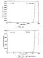
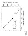
- Figure 1 gives the temperature profile of the treatment performed on the powder mixture as a function of time.
- the sintered pellets obtained were then polished with sandpaper to to obtain a final thickness of 1mm. Electrical contacts were then made by Au evaporation for electrical tests.
- the characteristics of the materials forming the varistors have been determined in the following manner.
- the size of ZnO crystallites was evaluated from the peak (100), curves X-ray diffraction patterns taken with a Siemens D-5000 diffractometer using radiation Cu-K ⁇ , positioned at 31.8 ° using Scherrer's formula.
- the microstructure of the pellets was examined with a microscope scanning electronics (JEOL JSN 840A and HITACHI S-570) equipped with a image analyzer. Grain size was evaluated from micrographs obtained.
- the overall chemical composition of the material thus obtained is as follows: ZnO 90.495 mole% Bi 2 O 3 3 mole% Sb 2 O 3 2% mole SiO 2 2% mole MnO 2 2.5 mole% Al 2 O 3 0.005 mole%
- a first mixture of Bi 2 O 3 was made with all the other additives chosen, namely Sb 2 O 3 , MnO 2 , SiO 2. and Al 2 O 3 .
- This first mixture was ground at high energy for 10 hours in a SPEX branded apparatus. This first ground mixture was then pressed at a pressure of 160 MPa so as to obtain a first pellet. This first pellet was then sintered at 1100 ° C. for 1 hour and then broken into pieces.
- the pieces of the first pellet were then mixed with the powder 99.99% pure ZnO.
- the second mixture thus obtained was milled at high energy for 10 hours in the same SPEX device.
- the second crushed mixture obtained was then calcined at 550 ° C. for 2.5 hours and mixed with 2% by weight of PVA used as a binder.
- the mixture of powder and PVA obtained was then pressed under form of a second pellet under a pressure of 630 MPa. This second pellet was sintered at 1000 ° C for 1 hour, then was cooled in the oven sintering.
- the second sintered pellet thus obtained was treated and then tested in the same manner. as in Example 1 and has been found to have substantially the same properties as but a much lower porosity (by a factor of 2) - see figure 16-.
- Example 2 Using the same starting materials and the same molar percentages as in Example 1, the procedure was essentially the same as in Example 2, except that in the first mixture prepared, it was excluded. ZnO doping agents, such as Al 2 O 3 , to be limited exclusively to materials known as "grain boundaries", namely Bi 2 O 3 , Sb 2 O 3 , MnO 2 and SiO 2 . This first mixture was subjected to the same first grinding, pressing and sintering as in Example 2, under the same conditions.
- ZnO doping agents such as Al 2 O 3
- the pure ZnO powder was crushed with its doping agent Al 2 O 3 for 10 hours in an SPEX apparatus, and the ground powder thus obtained was mixed with the pieces of the first sintered pellet obtained.
- This second mixture was then subjected to the same second grinding, calcination, addition of PVA, pressing and sintering as in Example 2.
- the second sintered pellet obtained as a final product has been found here again have substantially the same electrical properties as those obtained at Examples 1 and 2, but a much lower porosity than in Example 1.
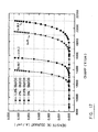
- FIG. 2a is a curve giving the value of the current density measured as a function of the field (V / cm) in the case of the S2-1000 varistor (2.5h) prepared according to Example 1.
- Figure 2b is a curve similar to Figure 2a, giving the value of the current density as a function of the field in the case of a varistor brand SEDIVER.
- the breakdown voltage of the S2-1000 varistor (2.5h) according to the invention is in the vicinity of 12.5 kV / cm and the ⁇ coefficient of non-linearity is 44.7.
- Leakage currents below the discharge threshold are in the range of 1 x 10 -7 to 2x10 -6 A / cm 2 .
- the leakage currents are illustrated in more detail in Figure 3a.
- the breakdown voltage of the SEDIVER conventional material is close to 2 kV / cm and its nonlinearity coefficient ⁇ is 45.2.
- Leakage currents below the discharge threshold are in the range of 1 x 10 -6 to 1 x 10 -4 A / cm 2 . These leakage currents are illustrated in Figure 3b, given for comparison.
- Figures 4 and 5 are curves similar to the curves of Figures 2a and 3a. These curves give the value of the current density according to the field as well as the value of the leakage currents of a varistor S2-1000 (0.5h) having exactly the same composition and prepared exactly the same way as the varistor S2-1000 (2.5h) of Example 1 except that the sintering time is 0.5h instead of 2.5h.
- the breakdown voltage is in the vicinity of 16 kV / cm, which proves that the shorter the sintering process, the less crystallites is affected and the breakdown voltage is high.
- sintering too short or not at a sufficiently high temperature or at a rate of heating too high does not solve porosity problems that can affect the quality of the varistors.
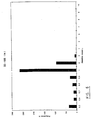
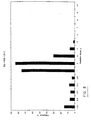
- FIGS. 6 to 9 give the size distribution of the ZnO grains and micrographs of these in the case of a S2-1000 varistor (1h) - see FIG. 6 and 7 - and a varistor S2-1000 (2h) - see Figures 8 and 9.
- the varistors had exactly the same composition than that of Example 1 and have been prepared in exactly the same way, if was that the sintering times at 1000 ° C were respectively 1h and 2h (instead 2.5h).
- the average grain diameter is of the order of 1 ⁇ m for the S2-1000 varistor (1h). This average diameter almost doubles in the case of varistors S2-1000 (2h). This again confirms that the duration of the sintering directly influences grain size and from there, should be as short as possible to get the best results.
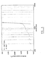
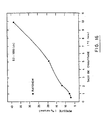
- FIG. 13 is a curve giving the value of the breakdown voltage in FIG. depending on the sintering time in the case of a S2-1000 varistor having the same composition than that of Example 1 and having been prepared exactly the same except for the sintering time at 1000 ° C.
- Figure 10 is a micrograph of the structure of the S2-1000 varistor (2.5h) prepared in Example 1.
- Figure 11 is a micrograph of the structure of a varistor S2-1200 (2.5h).
- round and black particles are ZnO. As can be seen, they typically have a size of 2 microns at 1000 ° C and are greater than 5 microns at 1200 ° C.
- FIG. 14 gives the value of the breakdown voltage in the case of varistors S2 and S3 as a function of the sintering temperature.
- the composition of these varistors was identical to that described in Example 1 (the supplement of SiO 2 was to the detriment of ZnO), and their preparation carried out in the same way except the sintering temperature.
- the breakdown voltage decreased from 12.2 kV / cm to 3.7 kV / cm between 1000 ° C and 1200 ° C.
- FIG. 16 is a curve giving the value of the porosity as a function of the heating rate in the case of a S2-1000 varistor (1h) having exactly the same composition as in Example 1 and having been prepared according to Example 2 with a calcination of 2,5h at 550 ° C, a pressing at 450 MPa and a sintering of 1h at 1000 ° C. The difference between each test was in the heating rate, that is to say the rate at which the powder-binder pressed mixture was heated to reach the selected sintering temperature of 1000 ° C.
- the heating rate has a strong influence on the porosity, which, to obtain a good varistor, must be as low as possible.
- the lower the heating rate the greater the porosity. low.
- the heating rate is too slow, we risk going too far time at high temperature, with the problem that this causes (see Example 5).
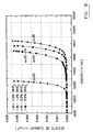
- FIG. 12 is a curve giving the value of the breakdown voltage in FIG. depending on the grinding time in the case of a S2-1000 varistor (2.5h) having exactly the same composition as that of Example 1, and having been prepared in the same way with the same equipment, if not the duration of the initial grinding.
- the breakdown voltage reaches a maximum about 12.5 kV / cm after 10 hours of grinding.
- This figure demonstrates the importance of intense mechanical grinding and therefore, the nanocrystalline structure obtained by the grinding on the properties of varistors.
- silica SiO 2 is a particularly useful additive insofar as it is known to inhibit grain growth.
- the breakdown voltage is inversely proportional to the size of the grains of ZnO.
- FIG. 15 illustrates the value of the current density as a function of the field, and from there, the breakdown voltage in the case of a varistor identical to that of Example 1, namely type S-1000 (2.5h), but in which the amount of silica (expressed in% mole) varied to the detriment of that of ZnO and for a duration of sintering of 1h.
- Figure 17 shows the influence of Sb 2 O 3 .
- Figure 18 shows the influence of MnO 2 .
- Figure 19 shows the influence of SnO 2 .
- Figure 20 shows the influence of Nb 2 O 5 .
Landscapes
- Engineering & Computer Science (AREA)
- Microelectronics & Electronic Packaging (AREA)
- Physics & Mathematics (AREA)
- Electromagnetism (AREA)
- Manufacturing & Machinery (AREA)
- Thermistors And Varistors (AREA)
- Compositions Of Oxide Ceramics (AREA)
- Battery Electrode And Active Subsutance (AREA)
Claims (27)
- Verfahren zur Herstellung eines Varistors mit sehr hoher Durchbruchspannung, mit folgenden Schritten:dadurch gekennzeichnet, dass die Verfestigungsbehandlung ein Sintern umfasst und mit so ausgewählten Temperatur- und Zeitbedingungen ausgeführt wird, dass gleichzeitig eine Größe der Zinkoxydkörner kleiner 3 Micron und eine geringe Porosität erhalten werden, wobei die Sintertemperatur zwischen 800°C und 1200°C liegt und die Behandlungszeit bei dieser Temperatur der Sinterung kleiner 2,5 Stunden beträgt.a) Zinkoxydpulver (ZnO) und Wismutoxydpulver (Bi2O3) werden mit mindestens einem weiteren Pulver eines Additivs gemischt, das in der Lage ist, die Eigenschaften der Varistoren zu beeinflussen; die Mischung wird mit solchen Anteilen der gewählten Pulver ausgeführt, dass das Zinkoxyd mindestens 75 Mol-% der Mischung ausmacht;b) die Pulver werden vor, während oder nach ihrer Mischung intensiv zermahlen, und zwar mittels einer mechanischen Mühle hoher Energie, damit die erhaltenen Pulver nanokristallin seien;c) die Mahl-Mischung wird einer Verfestigungsbehandlung unterworfen,
- Verfahren nach Anspruch 1,
dadurch gekennzeichnet, dass der Schritt b) der intensiven Zermahlung nach dem Schritt a) der Mischung der Pulver ausgeführt wird. - Verfahren nach Anspruch 1,
dadurch gekennzeichnet, dass vor der Mischung nach Schritt a) das Zinkoxydpulver, welches als Ausgangsmaterial verwendet wird, allein oder in Kombination mit einem oder mehreren Dotierungsmitteln zermahlen wird und dass das Wismutoxydpulver mit sämtlichen anderen Additiven vermischt wird, die so erhaltene Mischung von Wismutoxyd und den anderen Zusätzen danach zermahlen wird und bei hoher Temperatur behandelt wird. - Verfahren nach Anspruch 1, 2 oder 3,
dadurch gekennzeichnet, dassd) vor der Ausführung des Schrittes c) die Pulver oder deren Mischung bei einer Temperatur unterhalb oder gleich 550°C geröstet oder kalziniert werden. - Verfahren nach Anspruch 4,
dadurch gekennzeichnet, dasse) nach der Kalzinierung gemäß Schritt d) und vor der Durchführung des Schrittes c) in die Mischung der zermahlenen Pulver ein Bindemittel eingeführt wird, und dass die Mischung mit dem so zugeführten Bindemittel einer Verpressung unterworfen wird, um Pellets oder Tablette zu formen, die anschließend der Behandlung nach Schritt c) unterworfen werden. - Verfahren nach Anspruch 5,
dadurch gekennzeichnet, dass das Bindemittel aus Polyvynylalkohol besteht oder enthält und dass dieser Alkohol in die Pulvermischung durch mechanisches Zermahlen eingeführt wird. - Verfahren nach einem der Ansprüche 1 bis 6,
dadurch gekennzeichnet, dass die Verfestigungsbehandlung nach Schritt c) aus der Gruppe ausgewählt wird, die durch folgende Behandlungen gebildet wird: Verpressen, Walzen, Extrudieren, Ziehen, Spitzen und Injizieren, und dass der Verfestigungsschritt eine Wärmebehandlung einschließt oder eine solche nachfolgt. - Verfahren nach Anspruch 7,
dadurch gekennzeichnet, dass die Wärmebehandlung aus der Gruppe ausgewählt wird, die aus Aufheizung durch Konvektion, durch Induktion, durch Mikrowelle, durch Laserbestrahlung und durch elektrische Entladung gebildet wird. - Verfahren nach Anspruch 8,
dadurch gekennzeichnet, dass die Aufheizung durch eine oder mehrere Perioden kurzer Dauer bewirkt wird. - Verfahren nach einem der Ansprüche 1 bis 9,
dadurch gekennzeichnet, dass die Sinterung bei einer Temperatur in der Größenordnung von 1000°C ausgeführt wird. - Verfahren nach Anspruch 10,
dadurch gekennzeichnet, dass die Sinterung während einer Zeitperiode unterhalb oder gleich 1,5 Stunden ausgeführt wird. - Verfahren nach einem der Ansprüche 1 bis 11,
dadurch gekennzeichnet, dass die Sinterung mit einer Aufheizgeschwindigkeit bewirkt wird, die zwischen 0,5 und 10°C/min beträgt. - Verfahren nach Anspruch 12,
dadurch gekennzeichnet, dass die Sinterung mit einer Aufheizgeschwindigkeit in der Größenordnung von 1°C/min ausgeführt wird. - Verfahren nach einem der Ansprüche 1 bis 13,
dadurch gekennzeichnet, dass die zur Beeinflussung der Eigenschaften der Varistoren geeigneten Additive aus der Gruppe ausgewählt sind, die aus solchen Oxyden, Karbiden, Nitriden, Nitraten und Hydriden gebildet wird, die in der Lage sind, die Varistoren zu dotieren, deren Charakteristiken hinsichtlich Strom-Spannungskurve zu modifizieren, den spezifischen elektrischen Widerstand gegenüber Phasen zu modifizieren, den Verluststrom zu reduzieren, die Fähigkeit der Ableitung von Energie zu vergrößern, die Porosität zu steuern, das Kornwachstum zu verlangsamen, die strukturelle Integrität zu vergrößern, den Schmelzpunkt der unterschiedlichen Phasen zu ändern und ihre chemische, elektrische, mechanische und thermische Stabilität zu verbessern. - Verfahren nach Anspruch 14,
dadurch gekennzeichnet, dass das oder die Additive aus der Gruppe ausgewählt sind, die besteht aus den Oxyden Karbiden, Nitriden, Nitraten und Hydriden der folgenden Elemente: Si, Sb, Mn, Ge, Sn, Pb, Nb, B, Al, Ti, Ta, Fe, S, F, Li, Ni, Cr, Mo, W, Be, Br, Ba, Co, Pr, U, As, Ag, Mg, V, Cu, C, Zr, Se, Te und Ga. - Verfahren nach Anspruch 15,
dadurch gekennzeichnet, dass das oder die Additive aus der Gruppe ausgewählt sind, die besteht aus Antimonoxyd (Sb2O3), Manganoxyd (MnO2), Aluminiumoxyd (Al2O3), Siliciumoxyd (SiO2), Zinnoxyd (SnO2), Nioboxyd (Nb2O5), Kobaltoxyd (CoO oder Co3O4), Eisenoxyd (Fe2O3 oder Fe3O4) und Titanoxyd (TiO2 oder TiO). - Verfahren nach Anspruch 16,
dadurch gekennzeichnet, dass die in Schritt a) hergestellte Mischung umfasst:wobei der Rest durch ZnO gebildet wird.von 0,25 bis 10 Mol-% Bi2O3,von 1,5 bis 4 Mol-% Sb2O3,von 0,5 bis 4 Mol-% MnO2,von 0,00125 bis 0,05 Mol-% Al2O3,von 0 bis 4 Mol-% SiO2,von 0 bis 2 Mol-% SnO2,von 0 bis 2 Mol-% Nb2O5,von 0 bis 2,5 Mol-% CoO,von 0 bis 2,5 Mol-% Fe2O3 undvon 0 bis 3 Mol-% TiO2, - Verfahren nach Anspruch 17,
dadurch gekennzeichnet, dass die in Schritt a) hergestellte Mischung umfasst:90,495 Mol-% ZnO,3 Mol-% Bi2O3,2 Mol-% Sb2O3,2,5 Mol-% MnO2,2 Mol-% SiO2,0,005 Mol-% Al2O3. - Varistor auf der Basis von Zinkoxyd (ZnO) und Wismutoxyd (Bi2O3), wobei der Varistor mindestens 75 Mol-% ZnO enthält und eine schwache Porosität sowie eine sehr feine und homogene Mikrostruktur aufweist mit einer mittleren Größe der Körner von ZnO unterhalb von 3 Micron, wobei der Varistor eine Durchbruchsspannung oberhalb von 10 kV/cm aufweist, einen Koeffizienten α, der Nichtlinearität der Strom-Spannungskurve oberhalb von 20 aufweist, einen sehr schwachen Verluststrom unterhalb der Durchbruchsspannung besitzt und dadurch gekennzeichnet ist, dass er nach dem Verfahren nach einem der Ansprüche 1 bis 18 hergestellt worden ist.
- Varistor nach Anspruch 19,
dadurch gekennzeichnet, dass er in Form einer Tablette vorliegt. - Varistor nach Anspruch 19 oder 20,
dadurch gekennzeichnet, dass der Koeffizient α der Nichtlinearität der Strom-Spannungskurve oberhalb von 40 liegt. - Varistor nach Anspruch 21,
dadurch gekennzeichnet, dass der Koeffizient α oberhalb 60 liegt. - Varistor nach einem der Ansprüche 19 bis 22,
dadurch gekennzeichnet, dass er mindestens ein weiteres Pulver enthält, welches aus der Gruppe ausgewählt ist, welche durch solche Oxyde, Karbide, Nitride, Nitrate und Hydride gebildet wird, die in der Lage sind, die Varistoren zu dotieren, ihre Eigenschaften hinsichtlich Strom-Spannungskurve zu modifizieren, den spezifischen Widerstand der Phasen zu modifizieren, die Verlustströme zu verringern, die Fähigkeit der Ableitung von Energie zu vergrößern, die Porosität zu steuern, das Kornwachstum zu verlangsamen, die strukturelle Integrität zu vergrößern, den Schmelzpunkt der verschiedenen Phasen zu verändern und die chemische, elektrische, mechanische und thermische Stabilität zu verbessern. - Varistor nach Anspruch 23,
dadurch gekennzeichnet, dass die weiteren Pulver aus der Gruppe ausgewählt sind, die gebildet wird durch die Oxyde, Karbide, Nitride, Nitrate oder die Hydride der folgenden Elemente: Si, Sb, Mn, Ge, Sn, Pb, Nb, B, Al, Ti, Ta, Fe, S, F, Li, Ni, Cr, Mo, W, Be, Sr, Ba, Co, Pr, U, As, Ag, Mg, V, Cu, C, Zr, Se, Te und Ga. - Varistor nach Anspruch 24,
dadurch gekennzeichnet, dass die anderen Pulver aus der Gruppe ausgewählt sind, die gebildet wird durch Antimonoxyd (Sb2O3), Manganoxyd (MnO2), Aluminiumoxyd (Al2O3), Siliciumoxyd (SiO2), Zinnoxyd (SnO2), Nioboxyd (Nb2O5), Kobaltoxyd (CoO oder Co3O4), Eisenoxyd (Fe2O3 oder Fe3O4) und Titanoxyd (TiO2 oder TiO) . - Varistor nach Anspruch 25,
dadurch gekennzeichnet, dass er umfasst:wobei der Rest durch ZnO gebildet wird.von 0,25 bis 10 Mol-% Bi2O3,von 1,5 bis 4 Mol-% Sb2O3,von 0,5 bis 4 Mol-% MnO2,von 0,00125 bis 0,05 Mol-% Al2O3,von 0 bis 4 Mol-% SiO2,von 0 bis 2 Mol-% SnO2,von 0 bis 2 Mol-% Nb2O5,von 0 bis 2,5 Mol-% CoO,von 0 bis 2,5 Mol-% Fe2O3 undvon 0 bis 3 Mol-% TiO2, - Varistor nach Anspruch 26,
dadurch gekennzeichnet, dass er umfasst:90,495 Mol-% ZnO,3 Mol-% Bi2O3,2 Mol-% Sb2O3,2,5 Mol-% MnO2,2 Mol-% SiO2, und0,005 Mol-% Al2O3.
Applications Claiming Priority (3)
| Application Number | Priority Date | Filing Date | Title |
|---|---|---|---|
| CA002211813A CA2211813A1 (fr) | 1997-08-13 | 1997-08-13 | Varistances a base de poudres nanocristallines produites par broyage mecanique intense |
| CA2211813 | 1997-08-13 | ||
| PCT/CA1998/000769 WO1999009564A1 (fr) | 1997-08-13 | 1998-08-11 | Varistances a base de poudres nanocristallines produites par broyage mecanique intense |
Publications (2)
| Publication Number | Publication Date |
|---|---|
| EP1010186A1 EP1010186A1 (de) | 2000-06-21 |
| EP1010186B1 true EP1010186B1 (de) | 2004-04-07 |
Family
ID=4161140
Family Applications (1)
| Application Number | Title | Priority Date | Filing Date |
|---|---|---|---|
| EP98940000A Expired - Lifetime EP1010186B1 (de) | 1997-08-13 | 1998-08-11 | Varistoren auf basis von durch mechanische zerkleinerung hergestellten nanokristallpulvern |
Country Status (11)
| Country | Link |
|---|---|
| US (1) | US6620346B1 (de) |
| EP (1) | EP1010186B1 (de) |
| JP (1) | JP2001516142A (de) |
| KR (1) | KR20010022821A (de) |
| CN (1) | CN1269908A (de) |
| AT (1) | ATE264002T1 (de) |
| AU (1) | AU8846998A (de) |
| BR (1) | BR9811089A (de) |
| CA (1) | CA2211813A1 (de) |
| DE (1) | DE69823042T2 (de) |
| WO (1) | WO1999009564A1 (de) |
Families Citing this family (46)
| Publication number | Priority date | Publication date | Assignee | Title |
|---|---|---|---|---|
| US6832735B2 (en) * | 2002-01-03 | 2004-12-21 | Nanoproducts Corporation | Post-processed nanoscale powders and method for such post-processing |
| JP2001307909A (ja) | 2000-04-25 | 2001-11-02 | Toshiba Corp | 電流−電圧非直線抵抗体 |
| US6889216B2 (en) | 2002-03-12 | 2005-05-03 | Knowm Tech, Llc | Physical neural network design incorporating nanotechnology |
| US20040039717A1 (en) * | 2002-08-22 | 2004-02-26 | Alex Nugent | High-density synapse chip using nanoparticles |
| US7398259B2 (en) * | 2002-03-12 | 2008-07-08 | Knowmtech, Llc | Training of a physical neural network |
| US20030236760A1 (en) * | 2002-06-05 | 2003-12-25 | Alex Nugent | Multi-layer training in a physical neural network formed utilizing nanotechnology |
| US9269043B2 (en) | 2002-03-12 | 2016-02-23 | Knowm Tech, Llc | Memristive neural processor utilizing anti-hebbian and hebbian technology |
| US20040193558A1 (en) * | 2003-03-27 | 2004-09-30 | Alex Nugent | Adaptive neural network utilizing nanotechnology-based components |
| US7392230B2 (en) * | 2002-03-12 | 2008-06-24 | Knowmtech, Llc | Physical neural network liquid state machine utilizing nanotechnology |
| US8156057B2 (en) * | 2003-03-27 | 2012-04-10 | Knowm Tech, Llc | Adaptive neural network utilizing nanotechnology-based components |
| US7412428B2 (en) * | 2002-03-12 | 2008-08-12 | Knowmtech, Llc. | Application of hebbian and anti-hebbian learning to nanotechnology-based physical neural networks |
| US7752151B2 (en) * | 2002-06-05 | 2010-07-06 | Knowmtech, Llc | Multilayer training in a physical neural network formed utilizing nanotechnology |
| US7827131B2 (en) * | 2002-08-22 | 2010-11-02 | Knowm Tech, Llc | High density synapse chip using nanoparticles |
| TW200410908A (en) * | 2002-12-23 | 2004-07-01 | Zhang Guo Ying | Zinc oxide component with nano powder structure and method for producing the same |
| US7426501B2 (en) * | 2003-07-18 | 2008-09-16 | Knowntech, Llc | Nanotechnology neural network methods and systems |
| KR20060044462A (ko) * | 2004-11-10 | 2006-05-16 | 학교법인 원광학원 | 산화아연 나노파우더 바리스터 및 그의 제조방법 |
| US7409375B2 (en) * | 2005-05-23 | 2008-08-05 | Knowmtech, Llc | Plasticity-induced self organizing nanotechnology for the extraction of independent components from a data stream |
| US7502769B2 (en) * | 2005-01-31 | 2009-03-10 | Knowmtech, Llc | Fractal memory and computational methods and systems based on nanotechnology |
| JP4246716B2 (ja) | 2005-05-02 | 2009-04-02 | Tdk株式会社 | 積層型フィルタ |
| US7420396B2 (en) * | 2005-06-17 | 2008-09-02 | Knowmtech, Llc | Universal logic gate utilizing nanotechnology |
| US7599895B2 (en) | 2005-07-07 | 2009-10-06 | Knowm Tech, Llc | Methodology for the configuration and repair of unreliable switching elements |
| US20080128274A1 (en) * | 2006-12-04 | 2008-06-05 | Honeywell International Inc. | Nanostructured sensor for high temperature applications |
| US7930257B2 (en) | 2007-01-05 | 2011-04-19 | Knowm Tech, Llc | Hierarchical temporal memory utilizing nanotechnology |
| JP4893371B2 (ja) * | 2007-03-02 | 2012-03-07 | Tdk株式会社 | バリスタ素子 |
| JP5150111B2 (ja) * | 2007-03-05 | 2013-02-20 | 株式会社東芝 | ZnOバリスター粉末 |
| US20090143216A1 (en) * | 2007-12-03 | 2009-06-04 | General Electric Company | Composition and method |
| US20090142590A1 (en) * | 2007-12-03 | 2009-06-04 | General Electric Company | Composition and method |
| TWI402864B (zh) * | 2008-07-11 | 2013-07-21 | Sfi Electronics Technology Inc | 一種氧化鋅變阻器的製法 |
| US8693012B2 (en) * | 2008-09-04 | 2014-04-08 | Xerox Corporation | Run cost optimization for multi-engine printing system |
| JP5208703B2 (ja) | 2008-12-04 | 2013-06-12 | 株式会社東芝 | 電流−電圧非直線抵抗体およびその製造方法 |
| US20100157492A1 (en) * | 2008-12-23 | 2010-06-24 | General Electric Company | Electronic device and associated method |
| CN101630553B (zh) * | 2009-07-17 | 2011-10-12 | 立昌先进科技股份有限公司 | 一种氧化锌变阻器的制备方法 |
| EP2305622B1 (de) * | 2009-10-01 | 2015-08-12 | ABB Technology AG | Varistormaterial mit hoher Feldstärke-Festigkeit |
| JP5674317B2 (ja) * | 2010-01-13 | 2015-02-25 | コーア株式会社 | 酸化亜鉛バリスタおよびその製造方法 |
| EP2645380A1 (de) * | 2012-03-30 | 2013-10-02 | Inael Electrical Systems, S.A. | Verfahren zum Erhalten dotierter Zinkoxid-Varistoren, das Produkt aus dem Verfahren und seine Verwendung |
| CN111718192B (zh) * | 2012-12-27 | 2023-07-21 | 东莞令特电子有限公司 | 基于氧化锌的变阻器和制造方法 |
| US9876342B2 (en) | 2013-09-25 | 2018-01-23 | 3M Innovative Properties Company | Compositions for electric field grading |
| CN104658727B (zh) * | 2013-11-22 | 2017-07-07 | 华中科技大学 | 一种贱金属内电极叠层片式ZnO压敏电阻器及其制备方法 |
| CN104086170B (zh) * | 2014-06-11 | 2015-10-28 | 广东风华高新科技股份有限公司 | 低压压敏电阻陶瓷片及其制备方法、低压压敏电阻器的制备方法 |
| JP7169776B2 (ja) | 2018-06-06 | 2022-11-11 | Koa株式会社 | 酸化亜鉛バリスタおよびその製造方法 |
| KR102208539B1 (ko) * | 2018-12-17 | 2021-01-27 | 한국세라믹기술원 | ZnO계 바리스터 조성물 및 그 제조 방법과, 그 바리스터 |
| KR102209468B1 (ko) * | 2018-12-17 | 2021-01-29 | 한국세라믹기술원 | ZnO계 바리스터 조성물 및 그 제조 방법과, 그 바리스터 |
| KR102209467B1 (ko) * | 2018-12-17 | 2021-01-29 | 한국세라믹기술원 | ZnO계 바리스터 조성물 및 그 제조 방법과, 그 바리스터 |
| KR102209469B1 (ko) * | 2018-12-17 | 2021-01-29 | 한국세라믹기술원 | ZnO계 바리스터 조성물 및 그 제조 방법과, 그 바리스터 |
| KR102666011B1 (ko) * | 2019-07-10 | 2024-05-16 | 한국전력공사 | ZnO계 바리스터 조성물과 이의 제조방법 및 바리스터 |
| CN114477994A (zh) * | 2022-01-25 | 2022-05-13 | 广东爱晟电子科技有限公司 | 一种大功率陶瓷芯片电阻及其材料和制备 |
Family Cites Families (6)
| Publication number | Priority date | Publication date | Assignee | Title |
|---|---|---|---|---|
| US4094061A (en) * | 1975-11-12 | 1978-06-13 | Westinghouse Electric Corp. | Method of producing homogeneous sintered ZnO non-linear resistors |
| DE3335354A1 (de) * | 1983-09-29 | 1985-04-18 | Siemens AG, 1000 Berlin und 8000 München | Verfahren zur herstellung dotierter zinkoxid-varistor-keramik |
| US4681717A (en) | 1986-02-19 | 1987-07-21 | The United States Of America As Represented By The United States Department Of Energy | Process for the chemical preparation of high-field ZnO varistors |
| US5905000A (en) * | 1996-09-03 | 1999-05-18 | Nanomaterials Research Corporation | Nanostructured ion conducting solid electrolytes |
| US5952040A (en) * | 1996-10-11 | 1999-09-14 | Nanomaterials Research Corporation | Passive electronic components from nano-precision engineered materials |
| JPH11297510A (ja) * | 1998-04-07 | 1999-10-29 | Murata Mfg Co Ltd | 積層型バリスタ |
-
1997
- 1997-08-13 CA CA002211813A patent/CA2211813A1/fr not_active Abandoned
-
1998
- 1998-08-11 AT AT98940000T patent/ATE264002T1/de not_active IP Right Cessation
- 1998-08-11 CN CN98809021A patent/CN1269908A/zh active Pending
- 1998-08-11 EP EP98940000A patent/EP1010186B1/de not_active Expired - Lifetime
- 1998-08-11 DE DE69823042T patent/DE69823042T2/de not_active Expired - Fee Related
- 1998-08-11 WO PCT/CA1998/000769 patent/WO1999009564A1/fr not_active Ceased
- 1998-08-11 BR BR9811089-6A patent/BR9811089A/pt not_active IP Right Cessation
- 1998-08-11 AU AU88469/98A patent/AU8846998A/en not_active Abandoned
- 1998-08-11 KR KR1020007001423A patent/KR20010022821A/ko not_active Ceased
- 1998-08-11 US US09/485,401 patent/US6620346B1/en not_active Expired - Fee Related
- 1998-08-11 JP JP2000510145A patent/JP2001516142A/ja active Pending
Also Published As
| Publication number | Publication date |
|---|---|
| AU8846998A (en) | 1999-03-08 |
| JP2001516142A (ja) | 2001-09-25 |
| US6620346B1 (en) | 2003-09-16 |
| CA2211813A1 (fr) | 1999-02-13 |
| CN1269908A (zh) | 2000-10-11 |
| DE69823042D1 (de) | 2004-05-13 |
| BR9811089A (pt) | 2000-09-12 |
| ATE264002T1 (de) | 2004-04-15 |
| DE69823042T2 (de) | 2005-03-10 |
| WO1999009564A1 (fr) | 1999-02-25 |
| KR20010022821A (ko) | 2001-03-26 |
| EP1010186A1 (de) | 2000-06-21 |
Similar Documents
| Publication | Publication Date | Title |
|---|---|---|
| EP1010186B1 (de) | Varistoren auf basis von durch mechanische zerkleinerung hergestellten nanokristallpulvern | |
| LaCourse et al. | Characterization of the firing schedule for positive temperature coefficient of resistance BaTiO3 | |
| EP2194541B1 (de) | Strom-Spannung nichtlinearer Widerstand und Herstellungsverfahren dafür | |
| EP2622613A1 (de) | Yttrium-eisen-granatferrit, mikrowellenkomponente mit diesem ferrit sowie verfahren zur herstellung dieses ferrits und dieser komponente | |
| CN102034581B (zh) | 高场强度变阻器材料 | |
| JPH0812807B2 (ja) | 電圧非直線抵抗体及びその製造方法 | |
| CA2299167C (fr) | Varistances a base de poudres nanocristallines produites par broyage mecanique intense | |
| FR2818969A1 (fr) | Materiau ceramique dielectrique et son procede de fabrication | |
| EP3039694B1 (de) | Verfahren zur herstellung einer monolithischen elektromagnetischen komponente | |
| Alamdari et al. | High energy ball milled nanocrystalline ZnO varistors | |
| EP1683880A2 (de) | Verfahren zur Herstellung von Metalloxidhalbleiterkeramik, insbesondere Zinnoxid, speziell für Varistoren | |
| EP0067092B1 (de) | Dielektrische Keramikzusammensetzung auf der Basis von Bariumtitanat, Lithiumoxid und Kupferfluorid, Kondensator diese Zusammensetzung verwendend und Verfahren zur Herstellung der Zusammensetzung | |
| JPH0834136B2 (ja) | 電圧非直線抵抗体 | |
| EP2016596B1 (de) | Verwendung von b2o3 in einer halbleitenden keramik auf der basis von zinnoxid zur verringerung des leckstroms und zur stabilisierung der elektrischen eigenschaften | |
| JP4582851B2 (ja) | 電圧非直線抵抗体、並びにこの電圧非直線抵抗体を用いた避雷器 | |
| JP2011171665A (ja) | 電流−電圧非直線抵抗体およびその製造方法 | |
| FR2678605A1 (fr) | Composition de ceramique dielectrique. | |
| JP3337737B2 (ja) | 電圧依存性非直線抵抗体の製造方法 | |
| JP7359329B1 (ja) | 酸化アンチモン代替酸化亜鉛素子 | |
| KR102615494B1 (ko) | ZnO계 바리스터 조성물과, 그 바리스터 및 이의 제조 방법 | |
| JP2008100856A (ja) | 酸化亜鉛積層チップバリスタの製造方法 | |
| JP2024157203A (ja) | 電流-電圧非直線抵抗体、および、その製造方法 | |
| JPH09246016A (ja) | 非直線抵抗体 | |
| EP0243256A1 (de) | Zusammenstellungen für Thermistoren mit negativen Temperaturkoeffizienten | |
| WO2006077355A1 (fr) | Procede de preparation de ceramiques semi-conductrices constituees d'oxydes de metaux tel que l'etain en particulier pour les varistances |
Legal Events
| Date | Code | Title | Description |
|---|---|---|---|
| PUAI | Public reference made under article 153(3) epc to a published international application that has entered the european phase |
Free format text: ORIGINAL CODE: 0009012 |
|
| 17P | Request for examination filed |
Effective date: 20000302 |
|
| AK | Designated contracting states |
Kind code of ref document: A1 Designated state(s): AT BE CH CY DE DK ES FR GB IT LI NL PT SE |
|
| 17Q | First examination report despatched |
Effective date: 20011008 |
|
| GRAP | Despatch of communication of intention to grant a patent |
Free format text: ORIGINAL CODE: EPIDOSNIGR1 |
|
| GRAS | Grant fee paid |
Free format text: ORIGINAL CODE: EPIDOSNIGR3 |
|
| GRAA | (expected) grant |
Free format text: ORIGINAL CODE: 0009210 |
|
| AK | Designated contracting states |
Kind code of ref document: B1 Designated state(s): AT BE CH DE DK ES FR GB IT LI NL PT SE |
|
| PG25 | Lapsed in a contracting state [announced via postgrant information from national office to epo] |
Ref country code: NL Free format text: LAPSE BECAUSE OF FAILURE TO SUBMIT A TRANSLATION OF THE DESCRIPTION OR TO PAY THE FEE WITHIN THE PRESCRIBED TIME-LIMIT Effective date: 20040407 Ref country code: AT Free format text: LAPSE BECAUSE OF FAILURE TO SUBMIT A TRANSLATION OF THE DESCRIPTION OR TO PAY THE FEE WITHIN THE PRESCRIBED TIME-LIMIT Effective date: 20040407 |
|
| RBV | Designated contracting states (corrected) |
Designated state(s): AT BE CH DE DK ES FR GB IT LI NL PT SE |
|
| REG | Reference to a national code |
Ref country code: GB Ref legal event code: FG4D Free format text: NOT ENGLISH |
|
| REG | Reference to a national code |
Ref country code: CH Ref legal event code: EP |
|
| REF | Corresponds to: |
Ref document number: 69823042 Country of ref document: DE Date of ref document: 20040513 Kind code of ref document: P |
|
| PG25 | Lapsed in a contracting state [announced via postgrant information from national office to epo] |
Ref country code: DK Free format text: LAPSE BECAUSE OF FAILURE TO SUBMIT A TRANSLATION OF THE DESCRIPTION OR TO PAY THE FEE WITHIN THE PRESCRIBED TIME-LIMIT Effective date: 20040707 |
|
| PG25 | Lapsed in a contracting state [announced via postgrant information from national office to epo] |
Ref country code: ES Free format text: LAPSE BECAUSE OF FAILURE TO SUBMIT A TRANSLATION OF THE DESCRIPTION OR TO PAY THE FEE WITHIN THE PRESCRIBED TIME-LIMIT Effective date: 20040718 |
|
| REG | Reference to a national code |
Ref country code: SE Ref legal event code: TRGR |
|
| PG25 | Lapsed in a contracting state [announced via postgrant information from national office to epo] |
Ref country code: GB Free format text: LAPSE BECAUSE OF NON-PAYMENT OF DUE FEES Effective date: 20040811 |
|
| PG25 | Lapsed in a contracting state [announced via postgrant information from national office to epo] |
Ref country code: SE Free format text: LAPSE BECAUSE OF NON-PAYMENT OF DUE FEES Effective date: 20040812 |
|
| GBT | Gb: translation of ep patent filed (gb section 77(6)(a)/1977) |
Effective date: 20040728 |
|
| PG25 | Lapsed in a contracting state [announced via postgrant information from national office to epo] |
Ref country code: LI Free format text: LAPSE BECAUSE OF NON-PAYMENT OF DUE FEES Effective date: 20040831 Ref country code: CH Free format text: LAPSE BECAUSE OF NON-PAYMENT OF DUE FEES Effective date: 20040831 Ref country code: BE Free format text: LAPSE BECAUSE OF NON-PAYMENT OF DUE FEES Effective date: 20040831 |
|
| NLV1 | Nl: lapsed or annulled due to failure to fulfill the requirements of art. 29p and 29m of the patents act | ||
| PLBE | No opposition filed within time limit |
Free format text: ORIGINAL CODE: 0009261 |
|
| STAA | Information on the status of an ep patent application or granted ep patent |
Free format text: STATUS: NO OPPOSITION FILED WITHIN TIME LIMIT |
|
| BERE | Be: lapsed |
Owner name: *HYDRO-QUEBEC Effective date: 20040831 |
|
| PG25 | Lapsed in a contracting state [announced via postgrant information from national office to epo] |
Ref country code: DE Free format text: LAPSE BECAUSE OF NON-PAYMENT OF DUE FEES Effective date: 20050301 |
|
| EUG | Se: european patent has lapsed | ||
| 26N | No opposition filed |
Effective date: 20050110 |
|
| GBPC | Gb: european patent ceased through non-payment of renewal fee |
Effective date: 20040811 |
|
| REG | Reference to a national code |
Ref country code: CH Ref legal event code: PL |
|
| PG25 | Lapsed in a contracting state [announced via postgrant information from national office to epo] |
Ref country code: FR Free format text: LAPSE BECAUSE OF NON-PAYMENT OF DUE FEES Effective date: 20050429 |
|
| REG | Reference to a national code |
Ref country code: FR Ref legal event code: ST |
|
| PG25 | Lapsed in a contracting state [announced via postgrant information from national office to epo] |
Ref country code: IT Free format text: LAPSE BECAUSE OF NON-PAYMENT OF DUE FEES;WARNING: LAPSES OF ITALIAN PATENTS WITH EFFECTIVE DATE BEFORE 2007 MAY HAVE OCCURRED AT ANY TIME BEFORE 2007. THE CORRECT EFFECTIVE DATE MAY BE DIFFERENT FROM THE ONE RECORDED. Effective date: 20050811 |
|
| BERE | Be: lapsed |
Owner name: *HYDRO-QUEBEC Effective date: 20040831 |
|
| PG25 | Lapsed in a contracting state [announced via postgrant information from national office to epo] |
Ref country code: PT Free format text: LAPSE BECAUSE OF NON-PAYMENT OF DUE FEES Effective date: 20040907 |