EP1009033B1 - Piezoelektrisches Leuchtelement, elektronische Anzeigevorrichtung und dessen Herstellungsverfahren - Google Patents
Piezoelektrisches Leuchtelement, elektronische Anzeigevorrichtung und dessen Herstellungsverfahren Download PDFInfo
- Publication number
- EP1009033B1 EP1009033B1 EP19990124655 EP99124655A EP1009033B1 EP 1009033 B1 EP1009033 B1 EP 1009033B1 EP 19990124655 EP19990124655 EP 19990124655 EP 99124655 A EP99124655 A EP 99124655A EP 1009033 B1 EP1009033 B1 EP 1009033B1
- Authority
- EP
- European Patent Office
- Prior art keywords
- piezoelectric
- light
- pressure
- luminous
- luminous layer
- Prior art date
- Legal status (The legal status is an assumption and is not a legal conclusion. Google has not performed a legal analysis and makes no representation as to the accuracy of the status listed.)
- Expired - Lifetime
Links
Images
Classifications
-
- C—CHEMISTRY; METALLURGY
- C09—DYES; PAINTS; POLISHES; NATURAL RESINS; ADHESIVES; COMPOSITIONS NOT OTHERWISE PROVIDED FOR; APPLICATIONS OF MATERIALS NOT OTHERWISE PROVIDED FOR
- C09K—MATERIALS FOR MISCELLANEOUS APPLICATIONS, NOT PROVIDED FOR ELSEWHERE
- C09K11/00—Luminescent, e.g. electroluminescent, chemiluminescent materials
- C09K11/06—Luminescent, e.g. electroluminescent, chemiluminescent materials containing organic luminescent materials
-
- G—PHYSICS
- G01—MEASURING; TESTING
- G01N—INVESTIGATING OR ANALYSING MATERIALS BY DETERMINING THEIR CHEMICAL OR PHYSICAL PROPERTIES
- G01N21/00—Investigating or analysing materials by the use of optical means, i.e. using sub-millimetre waves, infrared, visible or ultraviolet light
- G01N21/62—Systems in which the material investigated is excited whereby it emits light or causes a change in wavelength of the incident light
- G01N21/70—Systems in which the material investigated is excited whereby it emits light or causes a change in wavelength of the incident light mechanically excited, e.g. triboluminescence
-
- Y—GENERAL TAGGING OF NEW TECHNOLOGICAL DEVELOPMENTS; GENERAL TAGGING OF CROSS-SECTIONAL TECHNOLOGIES SPANNING OVER SEVERAL SECTIONS OF THE IPC; TECHNICAL SUBJECTS COVERED BY FORMER USPC CROSS-REFERENCE ART COLLECTIONS [XRACs] AND DIGESTS
- Y10—TECHNICAL SUBJECTS COVERED BY FORMER USPC
- Y10T—TECHNICAL SUBJECTS COVERED BY FORMER US CLASSIFICATION
- Y10T29/00—Metal working
- Y10T29/42—Piezoelectric device making
-
- Y—GENERAL TAGGING OF NEW TECHNOLOGICAL DEVELOPMENTS; GENERAL TAGGING OF CROSS-SECTIONAL TECHNOLOGIES SPANNING OVER SEVERAL SECTIONS OF THE IPC; TECHNICAL SUBJECTS COVERED BY FORMER USPC CROSS-REFERENCE ART COLLECTIONS [XRACs] AND DIGESTS
- Y10—TECHNICAL SUBJECTS COVERED BY FORMER USPC
- Y10T—TECHNICAL SUBJECTS COVERED BY FORMER US CLASSIFICATION
- Y10T29/00—Metal working
- Y10T29/49—Method of mechanical manufacture
- Y10T29/49002—Electrical device making
- Y10T29/49117—Conductor or circuit manufacturing
- Y10T29/49124—On flat or curved insulated base, e.g., printed circuit, etc.
- Y10T29/49155—Manufacturing circuit on or in base
- Y10T29/49156—Manufacturing circuit on or in base with selective destruction of conductive paths
Definitions
- the present invention relates to the use of a luminous element which can be used for, for example, a display device.
- US 3,828,186 an apparatus for intensifying radiation images is known. It comprises a phosphor layer and piezoelectric layer provided in between electrodes.
- phosphor any of the known phosphors which emit radiation energy when excited such as by application of energy thereto through friction, electron bombardment, application of an electric field or the like may be used.
- JP60118000 discloses a light emitting piezoelectric element comprising a back electrode, a piezoelectric layer, a fluorescent layer and an electrode, the whole encapsulated with a transparent and dampproof film.
- the inventor of this application has devised a specific structure to realize a luminous element and a display device, which utilize this tribo-luminescence phenomenon, and a method for manufacturing the luminous element and the display device.
- This invention relates to the use of a piezoelectric luminous element comprising:
- the pressure luminous layer is formed with any one luminescent material selected from a group consisting of N-isopropylcarbazole, silicon oxide glass, and Eu(TTA) 3 .
- the pressure luminous layer and the piezoelectric element may be held between substrates such that the distance between these substrates will not change. It is desirable that of the substrates, the substrate placed in contact with the side of the pressure luminous layer where the piezoelectric element is not provided be capable of transmitting light.
- a display device can comprise the piezoelectric luminous element, wherein the display device has a piezoelectric luminous unit, which is composed of at least the piezoelectric film, one of the electrodes, and the pressure luminous layer, and which is held between the substrates in a manner such that it can be activated independently in accordance with a picture element area.
- this display device may comprise a fluorescence conversion layer for converting the wavelength of the pressure luminous layer in accordance with the piezoelectric luminous unit on the substrate placed in contact with the light-emitting side of the pressure luminous layer.
- the display device may comprise a color filter for transmitting a specific wavelength in accordance with the piezoelectric luminous unit on the substrate placed in contact with the light-emitting side of the pressure luminous layer.
- a method for manufacturing a piezoelectric luminous element comprises the steps of:
- the step of forming the pressure luminous layer comprises the steps of:
- the step of forming the pressure luminous layer comprises the steps of:
- the step of forming the pressure luminous layer comprises the steps of:
- the step of forming the piezoelectric film comprises the steps of:
- crystallization is caused by laser irradiation, hyrothermal treatment in an alkali solution of fixed concentration or high temperature thermal treatment.
- a method for manufacturing a display device comprises the steps of:
- Example 1 not according to the invention relates to a basic structure of a luminous element which utilizes a tribo-luminescence phenomenon, and to a method for manufacturing such a luminous element.
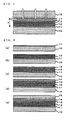
- Figure 1 is a sectional view of a piezoelectric luminous element used for this invention. White arrows in the drawing indicate the directions in which light is emitted.
- a piezoelectric luminous element 1 used for the invention comprises a substrate 10, an electrode film 11, a piezoelectric film 12, an electrode film 13, a pressure luminous layer 14, and a transparent substrate 15.
- the substrates 10 and 15 are composed of materials which have a certain degree of mechanical strength, such as silicon, various kinds of inorganic oxides (glass, quartz, magnesium oxide, zinc oxide), and resin. However, the substrate 15 placed on the side where light from the pressure luminous layer 14 should be transmitted has to be capable of transmitting light.
- the thickness of the substrates can be adjusted as appropriate in accordance with the specification of a relevant product.
- the electrode films 11 and 13 are the electrodes to apply voltage to the piezoelectric film 12. They are formed with conductive materials such as platinum (Pt), iridium (Ir), ITO (In 2 O 3 + 5% SnO 2 ), SnO 2 , In 2 O 3 , or ZnO. Each electrode film is formed with a thickness of, for example, about 200 nm.
- the piezoelectric film 12 is composed of crystals of normal piezoelectric ceramic.
- preferred materials are ferroelectric piezoelectric materials such as lead zirconate titanate (PZT), and such other materials obtained by adding metallic oxide such as niobium oxide, nickel oxide or magnesium oxide to the above-mentioned ferroelectric ceramic materials.
- the composition of the piezoelectric film 12 is selected as appropriate in consideration of the properties, usage, and other factors of the piezoelectric element.
- the thickness of the piezoelectric film is adjusted to the degree that allows the pressure luminous layer to emit sufficient light by means of displacements caused by the application of an electric field.
- the pressure luminous layer 14 is composed of materials that exhibit the tribo-luminescence phenomenon where the application of pressure causes the emission of light. For example, if N-isopropylcarbazole is used, it is possible to generate strong blue light (with a wavelength of 400 nm to 500 nm). If silicon oxide (SiO x : 0 ⁇ x ⁇ 2) glass is used, it is possible to generate blue light (with a wavelength of 430 nm), red light (with a wavelength of 630 nm), or white light (with a wavelength of 380 nm to 900 nm) in accordance with changes in the state of bonding between Si atoms and O atoms according to conditions of the film formation.
- silicon oxide (SiO x : 0 ⁇ x ⁇ 2) glass it is possible to generate blue light (with a wavelength of 430 nm), red light (with a wavelength of 630 nm), or white light (with a wavelength of 380 nm to 900 nm) in
- Eu (TTA) 3 it is possible to generate red light (with a wavelength of 610 nm). If phenanthrene is used, blue light with a wavelength of 400 nm to 440 nm can be obtained. If coumarin is used, light with wavelengths of 390 nm to 450 nm can be obtained. If m-aminophenol is used, ultraviolet rays with wavelengths of about 340 nm can be emitted, and it is thereby possible to use this invention for the irradiation of light other than visible light. If phthalic anhydride is used, light with wavelengths of 360 nm to 420 nm can be obtained.
- the application of a given voltage between the electrodes 11 and 13 generates an electric field between the electrodes, thereby causing the crystals of the piezoelectric film 12 to exhibit an electromechanical transducing action and to deform. Stress caused by this deformation act in the surface direction of the piezoelectric film.
- the displacement of the piezoelectric film directly deforms the pressure luminous layer 14. Deformation causes a strong electric field on the surface portion of the pressure luminous layer 14. This electric field activates N 2 existing in the vicinity of the surface, and light is emitted there. Moreover, this light activates the luminous layer material and other portions of the pressure luminous layer 14 also emit light.
- the application of pressure on the pressure luminous layer excites electrons in the pressure layer, and the pressure luminous layer thereby emits light when the energy level of electron returns to the ground state. This light is transmitted through the transparent substrate 15 and is then emitted externally.
- impurities and defects existing in tribo-luminescence materials, or rare earth elements added to the tribo-luminescence materials determine the light-emitting properties. Consequently, it is possible to adjust the color of the emitted light by adjusting such conditions.
- a method for manufacturing a piezoelectric element used for this invention is hereinafter explained with reference to Figure 2, sectional views illustrative of the manufacturing steps.
- the piezoelectric element forming step is the step of forming, over the surface of a substrate 10, a piezoelectric element which is composed of a piezoelectric film 12 held between electrode films 11 and 13.
- the electrode film 11 is formed over the substrate 10 ( Figure 2(a)).
- Example materials of the electrode film are platinum (Pt), iridium (Ir), ITO (In 2 O 3 + 5% SnO 2 ), SnO 2 , In 2 O 3 , and ZnO.
- the method for forming the electrode film a normal method for forming a conductive metal film is applied. For example, if Pt is used as the electrode film, a sputtering method is employed. If ITO is used as the electrode film, the sputtering method or an electron beam vapor deposition method is employed. As for the thickness of the electrode film 11, some hundreds of nanometers will suffice.
- the piezoelectric film 12 is formed ( Figure 2 (b)).
- a normally employed method for crystallizing piezoelectric ceramics is applied.
- a sol which is made of a starting materials for PZT, namely metal alkoxides, acetates and so on is applied by a coating method such as a spin coating method.
- drying is performed at a temperature of about 180°C for about 10 minutes and pyrolysis is then performed at a temperature of about 400°C for about 30 minutes.
- Such drying and pyrolysis causes the metal alkoxide in the sol and the acetate to undergo thermal decomposition of ligands, thereby forming a metal-oxygen-metal network.
- the above-described cycle is repeated for a certain number of times (for example, eight times) to laminate a multiplicity of piezoelectric thin films. After the piezoelectric thin films are laminated a certain number of times, crystallization is conducted to crystallize the laminated gel.
- the crystallization it is possible to adopt various methods such as a method of using a laser, a method of performing hydrothermal treatment, and a method of performing fast thermal treatment.
- a KrF laser with a light emission wavelength of 248 nm is used. This laser light is irradiated with 30 ns pulses and with the output of about 300-700 mJ/cm 2 .
- hydrothermal treatment the treatment is conducted at a temperature of about 130°C for about 90 minutes in an alkali solution (Ba(OH) 2 ) in concentration of about 0.05 mol.
- the electrode film 13 is formed ( Figure 2(c)). This electrode film is formed in the same manner as the electrode film 11.
- the pressure luminous layer forming step is the step of forming, over the piezoelectric element, the pressure luminous layer with a material that exhibits the tribo-luminescence phenomenon.
- An appropriate manufacturing method differs depending on the luminescent material to be used.
- N-isopropylcarbazole is used as the luminescent material
- N-isopropylcarbazole powder is first mixed into a binder resin.
- the resin with this powder mixed therein is then applied to the electrode film 13 of the piezoelectric element.
- the coating method it is possible to employ various kinds of coating methods which are normally used. For example, coating can be performed by printing.
- the applied resin is dried at a fixed temperature (for example, 100°C) and is thereby hardened. If a thermosetting resin is used as this resin, it is possible to harden it by heating.
- SiO x (0 ⁇ x ⁇ 2)
- an amorphous silicon film is first formed over the electrode film 13.
- Thermal treatment is given to this silicon film at a fixed temperature (for example, in the range of 800°C to 1200°C) in an oxygen atmosphere, thereby producing a silicon oxide glass film. It is possible to change the color of the emitted light into any of red, blue, and white colors by adjusting the bonding state between Si and O by changing the temperature of the above-described thermal treatment.
- polycarbonate is first mixed with a europium compound, thereby generating a methylene chloride solution.
- a europium compound For example, 90 wt% polycarbonate is mixed with 10 wt% europium. Then, this solution is applied to the electrode film 13. The applied solution is dried under certain conditions.
- the substrate 15 is attached to the pressure luminous layer as a last step. After the attachment of the substrate, some measure should be taken so that the distance d between the substrates 10 and 15 will not change freely, for example, by placing the laminated body obtained above in a housing that can keep and fix the distance d almost constant, or by molding the peripheries of the laminated body obtained above with a resin. It is certainly necessary to carry out wiring in order to apply an electric field to the piezoelectric element.
- the piezoelectric element applies pressure on the luminescent material, which exhibits the tribo-luminescence phenomenon, thereby generating pressure. Accordingly, it is possible to provide a luminous element which emits light without generating heat. Therefore, it is possible to provide a luminous element which does not generate heat.
- Example 1 by using N-isopropylcarbazole as the luminescent material, it is possible to cause the emission of strong blue light.
- Example 1 by using SiO x (0 ⁇ x ⁇ 2) glass as the luminescent material and by adjusting the manufacturing conditions, it is possible to cause the emission of light of various colors.
- Example 1 by using Eu(TTA) 3 , it is possible to cause the emission of red light.
- Example 2 not according to this invention relates to a display device composed of a luminous element which utilizes the tribo-luminescence phenomenon, and also to a method for manufacturing such a display device.
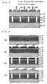
- Figure 3 is a sectional view of the display device of Example 2. Arrows in the drawing indicate the direction in which light is emitted.
- a display device 2 of this invention comprises a substrate 10, an electrode film 11, a piezoelectric film 12, an electrode film 13, a pressure luminous layer 14, a transparent substrate 15, and a color filter or fluorescence conversion layer 16.
- the substrate 10, the electrode film 11, the piezoelectric film 12, the electrode film 13, the pressure luminous layer 14, and the transparent substrate 15 can be considered as similar to those of Example 1.
- a multiplicity of electric field luminous units 1r, 1g, or 1b are provided, which are patterned in accordance with picture element areas composed of the piezoelectric film 12, the electrode film 13, and the pressure luminous layer 14. There is an appropriate gap between adjacent electric field luminous units.
- the color filter or fluorescence conversion layer 16 is a component which is required when it is desirable to adjust the wavelengths of light from the pressure luminous layer 14. For example, a color display device needs three primary colors of red, green, and blue.
- a color filter 16 is provided for transmitting the respective wavelengths corresponding to the primary colors contained in the white color.
- a red filter 16r is provided for a picture element corresponding to a red color
- a green filter 16g is provided for a picture element corresponding to a green color
- a blue filter 16b is provided for a picture element corresponding to a blue color.
- the color of the emitted light is blue and, therefore, it is necessary to change the color of the emitted light at the picture element corresponding to the red color and at the picture element corresponding to the green color.
- the fluorescence conversion layer 16 is used which is composed of a wavelength converting substance capable of absorbing the blue light and converting it into a red light, thereby causing the emission of the red light.
- perylene can be used as the wavelength converting substance for the red color.
- the fluorescence conversion layer 16 is used which is composed of a wavelength converting substance capable of absorbing the blue light and converting it into a green light, thereby causing the emission of the green light.
- a wavelength converting substance capable of absorbing the blue light and converting it into a green light, thereby causing the emission of the green light.
- coumarin 6 can be used as the wavelength converting substance for the green color.
- no fluorescence conversion layer is provided and the light from the pressure luminous layer is made to emit as it is.
- Other example materials of the fluorescence conversion layer are DCM1, quinacridone, rubrene, DCJT, and Nile red.
- the electrode film 11 Since the electrode film 11 is made to function as a common electrode, it is connected to an earth electrode of a drive circuit (not shown in the drawing).
- the electrode films 13 of the respective electric field luminous units are individually connected to drive terminals of the drive circuit.
- This structure relates to an active matrix system for activating the respective picture elements by means of active elements. If the display device is to be composed in a simple matrix system, it is necessary to pattern both the electrode films 11 and 13 independently in stripes and to carry out wiring in an X-Y matrix structure.
- any of the piezoelectric elements in the electric field luminous units (picture element areas) 1r, 1g, or 1b deforms. This deformation acts on the pressure luminous layer 14 in the relevant electric field luminous units, thereby exhibiting the tribo-luminescence phenomenon and causing the emission of light. If voltage is applied to the electric field luminous unit 1r corresponding to the red picture element, red light is emitted. If voltage is applied to the electric field luminous unit 1g corresponding to the green picture element, green light is emitted.
- a method for manufacturing the display device of Example 2 is hereinafter explained with reference to Figure 4, sectional views illustrative of the manufacturing steps.
- the step of forming the pressure luminous layer 14 ( Figure 4(a)) is similar to that of Example 1 ( Figures 2(a) through 2(d)).
- the subsequent step prior to the attachment of the substrate 15 is the step of conducting patterning for each picture element and dividing the relevant films into electric field luminous units.
- a photoresist 21 is first applied over the pressure luminous layer 14, and exposure and development are conducted in accordance with the pattern of the picture element areas, thereby leaving the photoresist 21 only in the picture element areas ( Figure 4(b)).
- a normal photolithography method can be employed. It is possible to arbitrarily select gaps between the picture element areas. However, if the gaps are too small and if the adjacent electric field luminous units are too close, the deformation at the time of activation may also cause the emission of light from the adjacent picture element areas. On the other hand, if the gaps are too large, the light emitting surface of the display device reduces and, therefore, the efficiency decreases. Appropriate gaps should be determined by keeping the above conditions in balance.
- Etching is then conducted to remove the pressure luminous layer 14, the electrode film 13, and the piezoelectric film 12 ( Figure 4(c)).
- the etching method either dry etching or wet etching may be employed. However, dry etching is preferred because it is possible to adjust the depth of etching delicately. It is necessary to control the depth of etching delicately so that the electrode film 11 can be left without being etched as the common electrode.
- the transparent substrate 15 is attached to the pressure luminous layer in the same manner as in Figure 2(e).
- the color filter or the fluorescence conversion layer 16 is formed in accordance with the colors set in the picture element areas. Whether the color filter or the fluorescence conversion layer should be adopted is determined in accordance with the color of the light emitted from the pressure luminous layer as stated above.
- the color filter pigments are mixed in a transparent resin or dyes are used, and patterning is then performed.
- a fluorescence converting material is applied to the pressure luminous layer, and patterning is then performed. Partitions may be formed between the picture element areas, and the materials for the color filter or the fluorescence converting materials may be selected to fill the respective picture element areas and may be dried.
- Example 2 can give the same advantageous effects as those of Example 1. Moreover, as it is composed to enable the emission of primary color light for each picture element, it is possible to provide a display device capable of realizing color display.
- the present invention is not limited to the respective embodiments described above and can be applied in many variations.
- materials for the pressure luminous layer are not limited to those mentioned in the above examples, but any materials that exhibit the tribo-luminescence phenomenon can be used.
- the layer structures of the piezoelectric luminous element and the display device are not limited to those described above, and it is possible to change the number of laminated layers and the arrangement of the layers in various ways. For example, if only one piezoelectric element cannot produce enough stress, it is possible to provide two or more piezoelectric elements and to make the stress from these piezoelectric elements simultaneously apply to the pressure luminous layer. As an example of such a structure, the pressure luminous layer may be held between two piezoelectric elements.
- This invention makes it possible to use a luminous element which utilizes the tribo-luminescence phenomenon and which has not been commercialized. Since the luminous element and the display device is not treated at high temperatures, it is possible to provide a light source with a small temperature increase and of high reliability.
- this piezoelectric luminous element As the intensity of the emitted light is detected, it is possible according to the invention to use this piezoelectric luminous element for the indirect measurement of displacement of the piezoelectric element.
Claims (1)
- Einsatz eines piezoelektrischen Leuchtelementes, das umfasst:eine Druck-Leuchtschicht (14) die bei der Ausübung von Druck Licht emittiert; undein piezoelektrisches Element, das einen piezoelektrischen Film (12) umfasst, zwischen Elektrodenfilmen (11, 13) aufgenommen ist und so angeordnet ist, dass es Druck auf die Druck-Leuchtschicht (14) ausüben kann,um die Verschiebung des piezoelektrischen Elementes durch Erfassen der Intensität des emittierten Lichtes zu messen.
Applications Claiming Priority (2)
| Application Number | Priority Date | Filing Date | Title |
|---|---|---|---|
| JP35107698 | 1998-12-10 | ||
| JP35107698A JP2000173301A (ja) | 1998-12-10 | 1998-12-10 | 圧電発光素子、表示装置およびそれらの製造方法 |
Publications (3)
| Publication Number | Publication Date |
|---|---|
| EP1009033A2 EP1009033A2 (de) | 2000-06-14 |
| EP1009033A3 EP1009033A3 (de) | 2004-07-21 |
| EP1009033B1 true EP1009033B1 (de) | 2006-06-21 |
Family
ID=18414888
Family Applications (1)
| Application Number | Title | Priority Date | Filing Date |
|---|---|---|---|
| EP19990124655 Expired - Lifetime EP1009033B1 (de) | 1998-12-10 | 1999-12-10 | Piezoelektrisches Leuchtelement, elektronische Anzeigevorrichtung und dessen Herstellungsverfahren |
Country Status (4)
| Country | Link |
|---|---|
| US (2) | US6281617B1 (de) |
| EP (1) | EP1009033B1 (de) |
| JP (1) | JP2000173301A (de) |
| DE (1) | DE69932023T2 (de) |
Families Citing this family (28)
| Publication number | Priority date | Publication date | Assignee | Title |
|---|---|---|---|---|
| GB9713074D0 (en) * | 1997-06-21 | 1997-08-27 | Cambridge Display Tech Ltd | Electrically-conducting colour filters for use in organic light-emitting displays |
| US6476406B1 (en) * | 1999-06-22 | 2002-11-05 | Agfa-Gevaert | Devices equipped with tribostimulable storage phosphors |
| US6420724B1 (en) * | 1999-06-22 | 2002-07-16 | Agfa-Gevaert | Method of image formation, dosimetry and personal monitoring |
| GB0119727D0 (en) | 2001-08-14 | 2001-10-03 | Qinetiq Ltd | Photoluminescent compounds |
| GB0119729D0 (en) * | 2001-08-14 | 2001-10-03 | Qinetiq Ltd | Triboluminescent materials and devices |
| KR20030039446A (ko) * | 2001-11-13 | 2003-05-22 | 삼성전자주식회사 | Fbar 제조방법 |
| US6710328B1 (en) | 2002-02-27 | 2004-03-23 | The United States Of America As Represented By The Secretary Of The Navy | Fiber optic composite damage sensor |
| JPWO2003078889A1 (ja) * | 2002-03-18 | 2005-07-14 | 独立行政法人科学技術振興機構 | 発光素子、表示装置、および応力センサ |
| JP2004071511A (ja) * | 2002-08-09 | 2004-03-04 | Sony Corp | 光導波路、光導波路装置、機械光学装置、検出装置、情報処理装置、入力装置、キー入力装置および繊維構造体 |
| KR100557144B1 (ko) | 2004-01-12 | 2006-03-03 | 삼성전자주식회사 | 시간 분할 다중화를 이용한 방송 통신 융합을 위한 이더넷수동형 광 가입자 망 |
| JP2005322421A (ja) * | 2004-05-06 | 2005-11-17 | Keiji Iimura | 応力発光素子および応力発光装置 |
| US7307702B1 (en) | 2004-08-13 | 2007-12-11 | The United States Of America As Represented By The Secretary Of The Navy | Color switchable stress-fracture sensor for damage control |
| KR100631968B1 (ko) | 2005-02-28 | 2006-10-11 | 삼성전기주식회사 | 파장변환형 발광장치 |
| JP5170356B2 (ja) * | 2005-03-22 | 2013-03-27 | セイコーエプソン株式会社 | 圧電素子及び液体噴射ヘッド並びに液体噴射装置 |
| JP2006303425A (ja) * | 2005-03-22 | 2006-11-02 | Seiko Epson Corp | 圧電素子及び液体噴射ヘッド並びに液体噴射装置 |
| JP2006350140A (ja) * | 2005-06-20 | 2006-12-28 | Nikon Corp | 表示装置及びこれに用いられるレジスト |
| JP4611268B2 (ja) * | 2006-09-22 | 2011-01-12 | 独立行政法人産業技術総合研究所 | 感圧デバイス |
| US8513883B2 (en) | 2008-12-31 | 2013-08-20 | Nokia Corporation | Electroluminescent device having piezoelectric component |
| US20140176615A1 (en) * | 2012-12-24 | 2014-06-26 | Uygar E. Avci | Transparent display using selective light filtering |
| US20150242057A1 (en) * | 2014-02-27 | 2015-08-27 | Samsung Display Co., Ltd. | Technique for generating localized light source for an embedded optical sensor array |
| CN105199711B (zh) * | 2015-09-08 | 2017-04-05 | 河南师范大学 | 咔唑衍生物作为摩擦发光材料在制作压感发光体或压力传感器中的应用 |
| DE102016205572A1 (de) * | 2016-04-05 | 2017-10-05 | Osram Gmbh | Akustischer sensor |
| KR101895681B1 (ko) * | 2016-10-21 | 2018-09-05 | 경북대학교 산학협력단 | 변형률을 표시하는 변형률 계측 센서 및 이의 제조 방법 |
| US11486774B2 (en) | 2018-10-19 | 2022-11-01 | The Florida State University Research Foundation, Inc. | Mechanoluminescent devices, articles, and methods |
| CN109443230B (zh) * | 2018-12-17 | 2021-01-12 | 东莞理工学院 | 一种基于图像处理的压电陶瓷测量系统 |
| CN110365246B (zh) * | 2019-07-10 | 2020-07-28 | 西安交通大学 | 一种微立体光刻制备柔性摩擦-压电复合式俘能器的方法 |
| KR102578055B1 (ko) * | 2020-04-03 | 2023-09-14 | 한국과학기술연구원 | 압전 발광소자를 이용한 초음파 이미징 시스템 및 방법 |
| CN113437239B (zh) * | 2021-06-24 | 2023-08-01 | 京东方科技集团股份有限公司 | 转移电荷的装置及显示设备 |
Family Cites Families (20)
| Publication number | Priority date | Publication date | Assignee | Title |
|---|---|---|---|---|
| US2905893A (en) * | 1954-05-14 | 1959-09-22 | Hurvitz Hyman | Visual indicators |
| GB913738A (en) * | 1960-02-05 | 1962-12-28 | Sylvania Thorn Colour Television Laboratories Ltd | Improvements relating to light-emitting and photo-sensitive devices |
| US3828186A (en) * | 1972-08-09 | 1974-08-06 | Vocon Inc | Apparatus for intensifying radiation images |
| JPS56136874A (en) * | 1980-03-31 | 1981-10-26 | Asahi Chem Ind Co Ltd | Tribo-luminous substance |
| JPS5831575U (ja) * | 1981-08-24 | 1983-03-01 | 株式会社横河電機製作所 | 表示装置 |
| US4532454A (en) * | 1983-09-16 | 1985-07-30 | Gte Laboratories Incorporated | Electroluminescent display having dark field semiconducting layer |
| JPS60118000A (ja) * | 1983-11-30 | 1985-06-25 | Sekonitsuku:Kk | 発光圧電素子 |
| JPS60124393A (ja) * | 1983-12-09 | 1985-07-03 | 日産自動車株式会社 | 多色発光薄膜elパネルの製造方法 |
| JPS63260087A (ja) * | 1986-12-26 | 1988-10-27 | Olympus Optical Co Ltd | 積層型圧電アクチュエータ |
| US5011816A (en) * | 1990-03-13 | 1991-04-30 | Eastman Kodak Company | Receiver for thermally-transferable fluorescent europium complexes |
| JPH06124807A (ja) * | 1992-10-13 | 1994-05-06 | Murata Mfg Co Ltd | 積層型チップ部品 |
| JPH0750418A (ja) * | 1993-08-06 | 1995-02-21 | Nissan Motor Co Ltd | 半導体装置の製造方法 |
| JP3710498B2 (ja) * | 1993-12-28 | 2005-10-26 | 株式会社リコー | 基板付き薄膜積層体の作製方法 |
| US5446334A (en) * | 1994-01-24 | 1995-08-29 | Gre, Incorporated | Piezoluminescent, pyroluminescent sensor |
| JPH0915886A (ja) * | 1995-06-27 | 1997-01-17 | Nec Corp | 電子写真用感光体の製造方法 |
| GB9523240D0 (en) * | 1995-11-14 | 1996-01-17 | Secr Defence | Damage sensors |
| JPH10261823A (ja) * | 1997-03-21 | 1998-09-29 | Citizen Watch Co Ltd | 強誘電体作製方法 |
| JPH10289784A (ja) * | 1997-04-14 | 1998-10-27 | Mitsubishi Chem Corp | 有機電界発光素子 |
| US6117574A (en) * | 1997-10-20 | 2000-09-12 | Agency Of Industrial Science And Technology | Triboluminescent inorganic material and a method for preparation thereof |
| US6207077B1 (en) * | 2000-02-18 | 2001-03-27 | Orion 21 A.D. Pty Ltd | Luminescent gel coats and moldable resins |
-
1998
- 1998-12-10 JP JP35107698A patent/JP2000173301A/ja active Pending
-
1999
- 1999-12-10 US US09/458,665 patent/US6281617B1/en not_active Expired - Lifetime
- 1999-12-10 EP EP19990124655 patent/EP1009033B1/de not_active Expired - Lifetime
- 1999-12-10 DE DE1999632023 patent/DE69932023T2/de not_active Expired - Lifetime
-
2001
- 2001-07-30 US US09/916,747 patent/US6571446B2/en not_active Expired - Lifetime
Also Published As
| Publication number | Publication date |
|---|---|
| EP1009033A2 (de) | 2000-06-14 |
| DE69932023D1 (de) | 2006-08-03 |
| US6281617B1 (en) | 2001-08-28 |
| US6571446B2 (en) | 2003-06-03 |
| DE69932023T2 (de) | 2006-11-02 |
| EP1009033A3 (de) | 2004-07-21 |
| JP2000173301A (ja) | 2000-06-23 |
| US20010054857A1 (en) | 2001-12-27 |
Similar Documents
| Publication | Publication Date | Title |
|---|---|---|
| EP1009033B1 (de) | Piezoelektrisches Leuchtelement, elektronische Anzeigevorrichtung und dessen Herstellungsverfahren | |
| JP5902212B2 (ja) | カラー・エレクトロルミネセンス表示装置 | |
| JP5793083B2 (ja) | 均一照射性を有する面発光光源 | |
| JP3578786B2 (ja) | Elラミネート誘電層構造体および該誘電層構造体生成方法ならびにレーザパターン描画方法およびディスプレイパネル | |
| JP2005513741A (ja) | エレクトロルミネセンス表示装置の薄膜層をパターン形成するレーザ・アブレーション法 | |
| US20060192213A1 (en) | Light-emitting device | |
| CN105518881A (zh) | 薄膜波长转换器以及用于制造薄膜波长转换器的方法 | |
| US6781304B2 (en) | EL panel | |
| JP2004031101A (ja) | 発光素子及び発光パネル | |
| JPWO2005122651A1 (ja) | 発光素子及び表示装置 | |
| JP2003217859A (ja) | Elパネル | |
| KR101163936B1 (ko) | 컬러 전계발광 디스플레이 | |
| JPH01149397A (ja) | エレクトロルミネッセンス素子 | |
| JP2006040642A (ja) | 色変換膜及びこれを用いたエレクトロルミネッセンス素子 | |
| JPH05299175A (ja) | El発光素子 | |
| JPH02168593A (ja) | 大画面多色表示装置 | |
| JP2003217860A (ja) | Elパネルおよびその製造方法 | |
| JP2000188182A (ja) | 紫外発光エレクトロルミネッセンス素子及び画像表示装置 | |
| TW563384B (en) | Electroluminescent laminate with patterned phosphor structure and thick film dielectric with improved dielectric properties | |
| JP2000195678A (ja) | 発光素子及び画像表示装置 | |
| JP2010197723A (ja) | 発光素子およびその製造方法、ならびに発光パネルおよび発光装置 | |
| JPS61160786A (ja) | El表示素子 | |
| JPH09167686A (ja) | 薄膜el素子 |
Legal Events
| Date | Code | Title | Description |
|---|---|---|---|
| PUAI | Public reference made under article 153(3) epc to a published international application that has entered the european phase |
Free format text: ORIGINAL CODE: 0009012 |
|
| AK | Designated contracting states |
Kind code of ref document: A2 Designated state(s): AT BE CH CY DE DK ES FI FR GB GR IE IT LI LU MC NL PT SE |
|
| AX | Request for extension of the european patent |
Free format text: AL;LT;LV;MK;RO;SI |
|
| PUAL | Search report despatched |
Free format text: ORIGINAL CODE: 0009013 |
|
| AK | Designated contracting states |
Kind code of ref document: A3 Designated state(s): AT BE CH CY DE DK ES FI FR GB GR IE IT LI LU MC NL PT SE |
|
| AX | Request for extension of the european patent |
Extension state: AL LT LV MK RO SI |
|
| 17P | Request for examination filed |
Effective date: 20040811 |
|
| 17Q | First examination report despatched |
Effective date: 20040922 |
|
| AKX | Designation fees paid |
Designated state(s): DE FR GB |
|
| GRAP | Despatch of communication of intention to grant a patent |
Free format text: ORIGINAL CODE: EPIDOSNIGR1 |
|
| RIC1 | Information provided on ipc code assigned before grant |
Ipc: G01B 11/16 20060101AFI20051220BHEP |
|
| GRAS | Grant fee paid |
Free format text: ORIGINAL CODE: EPIDOSNIGR3 |
|
| GRAA | (expected) grant |
Free format text: ORIGINAL CODE: 0009210 |
|
| AK | Designated contracting states |
Kind code of ref document: B1 Designated state(s): DE FR GB |
|
| REG | Reference to a national code |
Ref country code: GB Ref legal event code: FG4D |
|
| REF | Corresponds to: |
Ref document number: 69932023 Country of ref document: DE Date of ref document: 20060803 Kind code of ref document: P |
|
| ET | Fr: translation filed | ||
| PLBE | No opposition filed within time limit |
Free format text: ORIGINAL CODE: 0009261 |
|
| STAA | Information on the status of an ep patent application or granted ep patent |
Free format text: STATUS: NO OPPOSITION FILED WITHIN TIME LIMIT |
|
| 26N | No opposition filed |
Effective date: 20070322 |
|
| REG | Reference to a national code |
Ref country code: FR Ref legal event code: PLFP Year of fee payment: 17 |
|
| REG | Reference to a national code |
Ref country code: FR Ref legal event code: PLFP Year of fee payment: 18 |
|
| PGFP | Annual fee paid to national office [announced via postgrant information from national office to epo] |
Ref country code: FR Payment date: 20161111 Year of fee payment: 18 Ref country code: GB Payment date: 20161207 Year of fee payment: 18 Ref country code: DE Payment date: 20161206 Year of fee payment: 18 |
|
| REG | Reference to a national code |
Ref country code: DE Ref legal event code: R119 Ref document number: 69932023 Country of ref document: DE |
|
| GBPC | Gb: european patent ceased through non-payment of renewal fee |
Effective date: 20171210 |
|
| REG | Reference to a national code |
Ref country code: FR Ref legal event code: ST Effective date: 20180831 |
|
| PG25 | Lapsed in a contracting state [announced via postgrant information from national office to epo] |
Ref country code: DE Free format text: LAPSE BECAUSE OF NON-PAYMENT OF DUE FEES Effective date: 20180703 Ref country code: FR Free format text: LAPSE BECAUSE OF NON-PAYMENT OF DUE FEES Effective date: 20180102 |
|
| PG25 | Lapsed in a contracting state [announced via postgrant information from national office to epo] |
Ref country code: GB Free format text: LAPSE BECAUSE OF NON-PAYMENT OF DUE FEES Effective date: 20171210 |