EP1005986A1 - Flüssigkeitsausstossvorrichtung und verfahren zu ihrer hrestellung - Google Patents
Flüssigkeitsausstossvorrichtung und verfahren zu ihrer hrestellung Download PDFInfo
- Publication number
- EP1005986A1 EP1005986A1 EP99957038A EP99957038A EP1005986A1 EP 1005986 A1 EP1005986 A1 EP 1005986A1 EP 99957038 A EP99957038 A EP 99957038A EP 99957038 A EP99957038 A EP 99957038A EP 1005986 A1 EP1005986 A1 EP 1005986A1
- Authority
- EP
- European Patent Office
- Prior art keywords
- substrate
- ejection device
- fluid ejection
- ink
- hole
- Prior art date
- Legal status (The legal status is an assumption and is not a legal conclusion. Google has not performed a legal analysis and makes no representation as to the accuracy of the status listed.)
- Granted
Links
Images


Classifications
-
- B—PERFORMING OPERATIONS; TRANSPORTING
- B41—PRINTING; LINING MACHINES; TYPEWRITERS; STAMPS
- B41J—TYPEWRITERS; SELECTIVE PRINTING MECHANISMS, i.e. MECHANISMS PRINTING OTHERWISE THAN FROM A FORME; CORRECTION OF TYPOGRAPHICAL ERRORS
- B41J2/00—Typewriters or selective printing mechanisms characterised by the printing or marking process for which they are designed
- B41J2/005—Typewriters or selective printing mechanisms characterised by the printing or marking process for which they are designed characterised by bringing liquid or particles selectively into contact with a printing material
- B41J2/01—Ink jet
- B41J2/135—Nozzles
- B41J2/16—Production of nozzles
- B41J2/1621—Manufacturing processes
- B41J2/1623—Manufacturing processes bonding and adhesion
-
- B—PERFORMING OPERATIONS; TRANSPORTING
- B41—PRINTING; LINING MACHINES; TYPEWRITERS; STAMPS
- B41J—TYPEWRITERS; SELECTIVE PRINTING MECHANISMS, i.e. MECHANISMS PRINTING OTHERWISE THAN FROM A FORME; CORRECTION OF TYPOGRAPHICAL ERRORS
- B41J2/00—Typewriters or selective printing mechanisms characterised by the printing or marking process for which they are designed
- B41J2/005—Typewriters or selective printing mechanisms characterised by the printing or marking process for which they are designed characterised by bringing liquid or particles selectively into contact with a printing material
- B41J2/01—Ink jet
- B41J2/135—Nozzles
- B41J2/14—Structure thereof only for on-demand ink jet heads
- B41J2/14201—Structure of print heads with piezoelectric elements
- B41J2/14233—Structure of print heads with piezoelectric elements of film type, deformed by bending and disposed on a diaphragm
-
- B—PERFORMING OPERATIONS; TRANSPORTING
- B41—PRINTING; LINING MACHINES; TYPEWRITERS; STAMPS
- B41J—TYPEWRITERS; SELECTIVE PRINTING MECHANISMS, i.e. MECHANISMS PRINTING OTHERWISE THAN FROM A FORME; CORRECTION OF TYPOGRAPHICAL ERRORS
- B41J2/00—Typewriters or selective printing mechanisms characterised by the printing or marking process for which they are designed
- B41J2/005—Typewriters or selective printing mechanisms characterised by the printing or marking process for which they are designed characterised by bringing liquid or particles selectively into contact with a printing material
- B41J2/01—Ink jet
- B41J2/135—Nozzles
- B41J2/16—Production of nozzles
- B41J2/1607—Production of print heads with piezoelectric elements
- B41J2/161—Production of print heads with piezoelectric elements of film type, deformed by bending and disposed on a diaphragm
-
- B—PERFORMING OPERATIONS; TRANSPORTING
- B41—PRINTING; LINING MACHINES; TYPEWRITERS; STAMPS
- B41J—TYPEWRITERS; SELECTIVE PRINTING MECHANISMS, i.e. MECHANISMS PRINTING OTHERWISE THAN FROM A FORME; CORRECTION OF TYPOGRAPHICAL ERRORS
- B41J2/00—Typewriters or selective printing mechanisms characterised by the printing or marking process for which they are designed
- B41J2/005—Typewriters or selective printing mechanisms characterised by the printing or marking process for which they are designed characterised by bringing liquid or particles selectively into contact with a printing material
- B41J2/01—Ink jet
- B41J2/135—Nozzles
- B41J2/16—Production of nozzles
- B41J2/1621—Manufacturing processes
- B41J2/1626—Manufacturing processes etching
- B41J2/1628—Manufacturing processes etching dry etching
-
- B—PERFORMING OPERATIONS; TRANSPORTING
- B41—PRINTING; LINING MACHINES; TYPEWRITERS; STAMPS
- B41J—TYPEWRITERS; SELECTIVE PRINTING MECHANISMS, i.e. MECHANISMS PRINTING OTHERWISE THAN FROM A FORME; CORRECTION OF TYPOGRAPHICAL ERRORS
- B41J2/00—Typewriters or selective printing mechanisms characterised by the printing or marking process for which they are designed
- B41J2/005—Typewriters or selective printing mechanisms characterised by the printing or marking process for which they are designed characterised by bringing liquid or particles selectively into contact with a printing material
- B41J2/01—Ink jet
- B41J2/135—Nozzles
- B41J2/16—Production of nozzles
- B41J2/1621—Manufacturing processes
- B41J2/1631—Manufacturing processes photolithography
-
- B—PERFORMING OPERATIONS; TRANSPORTING
- B41—PRINTING; LINING MACHINES; TYPEWRITERS; STAMPS
- B41J—TYPEWRITERS; SELECTIVE PRINTING MECHANISMS, i.e. MECHANISMS PRINTING OTHERWISE THAN FROM A FORME; CORRECTION OF TYPOGRAPHICAL ERRORS
- B41J2/00—Typewriters or selective printing mechanisms characterised by the printing or marking process for which they are designed
- B41J2/005—Typewriters or selective printing mechanisms characterised by the printing or marking process for which they are designed characterised by bringing liquid or particles selectively into contact with a printing material
- B41J2/01—Ink jet
- B41J2/135—Nozzles
- B41J2/16—Production of nozzles
- B41J2/1621—Manufacturing processes
- B41J2/1632—Manufacturing processes machining
-
- B—PERFORMING OPERATIONS; TRANSPORTING
- B41—PRINTING; LINING MACHINES; TYPEWRITERS; STAMPS
- B41J—TYPEWRITERS; SELECTIVE PRINTING MECHANISMS, i.e. MECHANISMS PRINTING OTHERWISE THAN FROM A FORME; CORRECTION OF TYPOGRAPHICAL ERRORS
- B41J2/00—Typewriters or selective printing mechanisms characterised by the printing or marking process for which they are designed
- B41J2/005—Typewriters or selective printing mechanisms characterised by the printing or marking process for which they are designed characterised by bringing liquid or particles selectively into contact with a printing material
- B41J2/01—Ink jet
- B41J2/135—Nozzles
- B41J2/16—Production of nozzles
- B41J2/1621—Manufacturing processes
- B41J2/164—Manufacturing processes thin film formation
- B41J2/1646—Manufacturing processes thin film formation thin film formation by sputtering
-
- B—PERFORMING OPERATIONS; TRANSPORTING
- B41—PRINTING; LINING MACHINES; TYPEWRITERS; STAMPS
- B41J—TYPEWRITERS; SELECTIVE PRINTING MECHANISMS, i.e. MECHANISMS PRINTING OTHERWISE THAN FROM A FORME; CORRECTION OF TYPOGRAPHICAL ERRORS
- B41J2/00—Typewriters or selective printing mechanisms characterised by the printing or marking process for which they are designed
- B41J2/005—Typewriters or selective printing mechanisms characterised by the printing or marking process for which they are designed characterised by bringing liquid or particles selectively into contact with a printing material
- B41J2/01—Ink jet
- B41J2/135—Nozzles
- B41J2/14—Structure thereof only for on-demand ink jet heads
- B41J2002/14387—Front shooter
Definitions
- the present invention relates to a fluid ejection device to be used in a printhead of an ink jet printer for ejecting fluid such as ink in a well-controlled mariner, and production method thereof.
- the ink jet printhead of the on-demand system which enables a high-speed ejection of the ink at the user's will, is critical for the performance of the printer.
- the ink jet printhead in general, comprises an ink channel, a pressure chamber where ink is pressurized, a pressurizing means for the ink such as an actuator, and an ink outlet through which the ink is ejected.
- a pressurizing means with high controllability is required.
- Fig 11 is a sectional perspective view showing an example of the construction of a conventional ink jet printhead.
- the conventional ink jet printhead consists of a piezoelectric member 111, a pressure chamber 112, an ink channel 113, an ink outlet 114, a fluid (ink) inlet 115, a structure member A 116, a structure member B 117, a structure member C 118, a diaphragm 119 and individual electrodes 120 (120a, 120b).
- first side of the piezoelectric member 111 individual electrodes 120 are formed thereon. On a second side thereof electrodes are also formed in the same manner (not depicted). The piezoelectric member 111 is bonded to the diaphragm 119 via the electrode on the second side.
- the diaphragm 119 and the structure member A 116, the structure member B 117 and the structure member C 118 are bonded by an adhesive or similar material thereby forming a laminated structure.
- a plurality sets of the pressure chambers 112, the ink channel 113 and individual electrodes 120 are formed and disposed such that each set is separated from the other sets.
- the structure member B 117 is formed in the same manner with the ink inlet 115 being mounted additionally.
- the ink outlet 114 is mounted on the structure member C 118, corresponding to the position of the pressure chamber 112, the ink outlet 114 is mounted. The ink is supplied through the ink inlet 115, and the ink channel 113 and the pressure chamber 112 are filled with ink.
- the diaphragm 119 is made of a conductive material and has conductivity with the electrodes mounted on the bonded surface of the piezoelectric member 111. Thus, if an electric voltage is applied between the diaphragm 119 and the individual electrodes 120, the laminated section of the piezoelectric member 111 and the diaphragm 119 is deformed. At this time, an arbitrary location of the piezoelectric member 111, in other. words, the location corresponding to an arbitrary pressure chamber 112 can be deformed by selecting an electrode to be applied with an electric voltage.
- the deformation pressurizes ink in the pressure chamber 112, and the amount of ink responsive to the pressure is ejected from the ink outlet 114.
- the amount of deformation depends on the electric voltage applied to the piezoelectric member 111. Therefore, by controlling the magnitude of the electric voltage and the location on which the electric voltage is applied, amount and location of the ink ejection can be arbitrarily changed.
- the conventional thermal ink jet printhead in general, is inferior to the piezoelectric method in terms of the response speed.
- the displacement of the piezoelectric member and the diaphragm is restricted by the thickness of the piezoelectric member If the piezoelectric member is too thick, a sufficient displacement can not be gained due to the rigidity of the piezoelectric member itself. If the area of the piezoelectric member is increased to effect a sufficient displacement, the ink jet printhead will become bigger making harder to achieve a higher density of the nozzle. As a result, material cost will increase. When the area of the piezoelectric member can not be increased, a higher driving voltage is required for a sufficient deformation.
- a piezoelectric member with thickness of about 20 ⁇ m have become available now by techniques of the thick film forming and the integrated firing, however, a higher density in the nozzle is still required for an improved picture quality.
- reduction of the thickness of the piezoelectric member is essential.
- conventional methods have limitations in this regard.
- a cavity must be provided within the structures made of stainless steel or the like in order to form an ink channel, and for precise and complex ink channels. increased number of layers are required. Adhesive used on the bonded section is subjected to fluid for a long time, therefore, reliability of such material has always required close attention.
- An object of the present invention is to provide a fluid ejection device such as an ink jet printhead with higher picture quality, higher reliability and lower cost.
- a fluid ejection device of the present invention includes at least one chamber divided independently from other chambers, an ink channel communicating with the chamber, an ink outlet communicating with the chamber, and a pressure generating section having a laminated body made of a piezoelectric material of a thickness of not more than 7 ⁇ m and an elastic body, the section covering one face of the chamber.
- a production method of a fluid ejection device of the present invention includes the steps of: a process of forming a through-hole for the pressure chamber and a through-hole for the ink inlet on a first substrate; a process of bonding the first substrate and a second substrate; a process of bonding the second substrate and a third substrate; and a process of forming a pressure generating section comprising a laminated body including piezoelectric material and an elastic material such that the pressure generating section covers the through-hole for the pressure chamber.
- a thin film material of PZT related material deposited by sputtering method is used as a piezoelectric material.
- silicon and glass substrates are used as structure members which are etched and processed by sand-blasting.
- the structures are directly bonded by processing the surfaces and heating without the use of resin or other adhesives.
- the configuration discussed above allows the piezoelectric member to be thinner with ease, which contributes to a higher density of the nozzle.
- a plurality of silicon and glass substrates are simultaneously processed finely by etching and sand-blasting, thereby improving processing precision for products and reducing a number of production processes.
- the silicon and glass substrates can be directly bonded, therefore, long-term reliability against inflow of fluid is secured. Meanwhile, the substrates can be bonded at a time , which contributes to streamlining of the production processes.
- Fig. 1 is a perspective cross sectional view illustrating an example of a fluid ejection device comprising silicon, glass and piezoelectric thin films.
- a fluid ejection device in accordance with the first exemplary embodiment comprises the following elements; a piezoelectric thin film 11, a pressure chamber 12, an ink channel 13, an ink outlet 14, a through-hole 15, an ink inlet 16, a first silicon substrate 17, a glass substrate 18, a second silicon substrate 19, an elastic body 20 and individual electrodes 21(21a, 21b). More specifically, the fluid ejection device of this embodiment comprises a laminated body made of the first silicon substrate 17, the glass substrate 18 and the second silicon substrate 19, the piezoelectric thin film 11, the elastic body 20 and the individual electrodes 21 mounted on the piezoelectric thin film 11.
- the first silicon substrate 17 is provided with such elements as the pressure chamber 12 formed as an individual through-section at the position corresponding to the individual electrodes 21, the ink channel 13 formed up to the midway in the direction of the thickness of the silicon substrate 17 in such a manner that it communicates with the pressure chamber 12, and the ink inlet 16, a through-section communicating with the ink channel 13.
- the opening area of the ink channel 13 starts to expand outwardly as it goes away from the pressure chamber 12 (illustrated as dotted lines in Fig. 1).
- Fig. 1 shows a single set of the individual electrodes, the pressure chamber, and the ink outlet and so on.
- a fluid ejection device generally has a plurality of units constructed in a similar manner including the individual electrodes, the pressure chamber and the ink outlet Fig. 1 shows two sets of the individual electrodes 21 (21a and 21b).
- the glass substrate 18 is provided with a through-hole 15 on the position corresponding to the pressure chamber 12.
- an ink outlet 14 with an area smaller than the opening portion of the through-hole 15 is formed on the second silicon substrate 19.
- the piezoelectric thin film 11 is bonded through the elastic body 20 on the face of the pressure chamber 12 opposite the through-hole 15.
- the piezoelectric thin film 11 has the individual electrode 21a formed on front surface thereof, and other individual electrode on the back surface (not shown in the drawing).
- the fluid which has flowed in from the ink inlet 16 fills the ink channel 13, pressure chamber 12 and the through-hole 15, and stays around the ink outlet 14. If an. electric voltage is applied between the electrodes on both sides of the piezoelectric thin film 11, the laminated body of the piezoelectric thin film 11 and the elastic body 20 will be deformed.
- the elastic body 20 is made of a conducive material, it will conduct with the electrode mounted on the back face of the piezoelectric thin film, and deformation occurs when voltage is applied between the elastic body 20 and individual electrodes 21.
- the exact position of the laminated body to be deformed can be changed freely by selecting the portion of the individual electrode 21 to be applied with voltage.
- the deformation of the laminated body comprising the piezoelectric thin film 11 and the elastic body 20 brings the fluid in the pressure chamber 12 under pressure, and the fluid is ejected from the ink outlet 14 in a volume responsive to the strength of the pressure.
- a piezoelectric thin film 11 is made of material with high piezoelectric constant such as PbZr x Ti 1-x O 3 or other PZT related material.
- a thin film made of such material is manufactured, under certain condition, by depositing a film on a MgO substrate for the piezoelectric thin film by the sputtering method.
- the MgO substrate for the piezoelectric thin film is etched in phosphate or in a similar chemical whereby a thin film consisting of the piezoelectric thin film 11 is easily obtained.
- the shape of the ink outlet 14 affects ejection speed and the area of the ejected fluid, as such it is a key element determining the printing performance of an ink jet printer.
- a smaller opening area of the ink outlet 14 enables finer printing, however, an excessive difference in area from the pressure chamber would result in a large loss, thus desirable ejection can not be expected.
- This loss can be reduced when the glass substrate 18 is provided with the through-hole 15 of which a cross-sectional area tapers from the pressure chamber toward the ink outlet.
- this construction makes the shape of the ink outlet more controllable than a construction having a tapered hole alone, resulting in the ink outlet 14 with finer and more uniform shape.
- the ink channel 13 is shaped in a manner that its opening space (illustrated as dotted lines in Fig. 1) tapers toward the pressure chamber 12 thereby resistance against the back flow increases, and even a better ink ejection is achieved.
- the same effect can be obtained by providing a narrower section in the ink channel 13. When the area of the narrower section in the ink channel 13 is about 0.5 to 1.5 times as large as the area of the ink outlet 14, good ejection is secured by preventing the back flow.
- the piezoelectric thin film 11 of several ⁇ m in thickness can easily be obtained using the sputtering method. It is thinner when compared with conventional films. When the piezoelectric thin film 11 becomes thinner, its own rigidity is reduced, thus a larger deformation is more easily obtained. When the magnitude of deformation is the same, strain is smaller with the thinner film, therefore, reliability for repeated loading can be improved. As it has been described, the thinner piezoelectric material not only contributes to a reduced size of the actuator and its surrounding area and the area of the ink outlet 14, but also contributes to a higher density and in turn, a higher picture quality.
- a reasonable thickness of a piezoelectric thin film is not more than 7 ⁇ m in terms of a secure driving force and film making cost. Since the actuator is not deformed when it is only made of the piezoelectric thin film 11, it must form a laminated structure with the elastic body 20. In order for the elastic body 20 to actually function as the elastic body 20 while maintaining conductivity, stainless steel or other metallic material is used. However, the thickness of and the rigidity determined by nature of the material of each layer affect the position of the. neutral plane during deformation.
- the thickness of the elastic body made of metallic material must be the same or smaller than the thickness of the piezoelectric member.
- Each piezoelectric material has to function only for each pressure chamber, therefore, the piezoelectric material is not needed in the partitions of adjacent pressure chambers. Rather, when the piezoelectric material is separated by every pressure, interference between adjacent piezoelectric members and stress imposed on the piezoelectric material during the bonding process and actual driving can be avoided, so that cracking in the piezoelectric material is prevented.
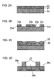
- Fig. 2 shows sectional views illustrating an example of the production method for dividing the piezoelectric material.
- a material for the individual electrode 23 and a piezoelectric thin film 22 are deposited on a MgO substrate for the piezoelectric thin film 24 by the sputtering method.
- the material for the individual electrode 23 and the piezoelectric thin film 22 are selectively etched away and divided into individual electrodes 23a, 23b and 23c, and piezoelectric thin films 22a, 22b and 22c respectively (Fig. 2B).
- an elastic body 28 made of chromium or other metallic material is formed with a resin material 25 such as polyimide coated thereon (Fig. 2C).
- a silicon substrate 27 is bonded to the dividing portion or the portion where the material for the individual electrode 23 and the piezoelectric thin film 22 are etched away selectively, in a manner that only pressure chambers 26a, 26b and 26c are correspondingly in contact with the piezoelectric thin films 22a, 22b and 22c.
- the MgO substrate for the piezoelectric thin film is immersed in a phosphate solution and removed (Fig. 2D).
- the dividing portions are strengthened by the resin material 25.
- the rigidity of the resin material 25 is low, it does not seriously affect the driving.
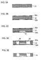
- FIGS. 3A-3E, Figs. 4A-4E and Figs. 5A-5D show sectional views illustrating the manufacturing process of the fluid ejection device of the present invention.
- Figs. 3A-3E show an example of the processing of the first silicon substrate 31. Both sides of a first silicon substrate 31 as shown in Fig. 3A are coated with resists 32a and 32b, and the patterning is carried out by the photolithography technique (Fig. 3B). In this process, patterns are formed corresponding to the position and shape of each pressure chamber 34 and ink channel 33.
- silicon is etched from the side coated with the resist 32b by the reactive ion etching method (RIE).
- RIE reactive ion etching method
- the etching stops at the predetermined depth in the direction of the thickness of the substrate with an opening being formed on only one side, forming an ink channel 33 (Fig. 3C).
- etching is performed from the resist 32a side forming a through-section communicating with the ink channel 33.
- a pressure chamber 34 and an ink inlet 35 are formed (Fig. 3D).
- the resists 32a and 32b are removed to conclude the manufacturing process of the first silicon substrate 31 (Fig. 3E).
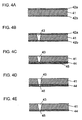
- Figs. 4A-4E show an example of a manufacturing process of a glass substrate 41 and a second silicon substrate 44.
- both sides of the glass substrate 41 are coated with resists 42a and 42b. Then, a pattern is formed only on the resist 42a side at a place corresponding to the pressure chamber (Fig. 4A). Next abrasive grains are sprayed by the sand-blasting method from the resist 42a side, and then a through-hole 43 is formed by processing the glass substrate 41. (Fig. 4B). In this process, the through-hole 43 is formed in a manner that it tapers from the side being sprayed with the abrasive grains toward the other opening. The resist 42b protects the other face from damage caused by the abrasive grains.
- the second silicon substrate 44 and the glass substrate 41 are directly bonded by direct bonding technique.
- Patterning of a resist 45 coated on the second silicon substrate 44 is processed so as to form an ink outlet 46 in corresponding positions to each pressure chamber (Fig. 4C).
- the direct bonding technique is a method to bond substrates by washing the substrates and heating them without using any inclusions such as resin or applying a high electric voltage as it is the case with the anodic bonding method.
- glass and silicon with a smooth surface are washed in peroxomonosulfuric acid, peroxodisulfuric or the like and stacked after drying.
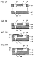
- Figs. 5A-5D show sectional views illustrating the bonding process of a laminated body comprising a processed first silicon substrate 56, a glass substrate 57 and a second silicon substrate 58 and a piezoelectric thin film 59 (including elastic body).
- the first silicon substrate 56 already processed in a manner illustrated in Figs. 3A-3E and the laminated body of the second silicon substrate 58 and the glass substrate 57 processed in a manner illustrated in Figs. 4A-4E are directly bonded by the same method described above (Fig. 5B).
- a pressure chamber 51 and a through-hole 54 are aligned.
- the piezoelectric thin film 59 (including an elastic body) formed on a substrate 60 made of MgO or the like for the piezoelectric thin film 60 is bonded onto the top of the pressure chamber 51 (Fig. 5C).
- the MgO substrate 60 for the piezoelectric thin film is removed to complete the process (Fig. 5D).
- the substrate 60 for the piezoelectric thin film is made of MgO, it can be removed by immersing it in a phosphate solution and the like.
- a micro-fabrication technique can be adopted to realize a high-precision and high-efficiency processing. Moreover, bonding process is simple and the end product is highly reliable. When the sand-blasting is used, fragile material such as glass can be processed rapidly with the through-hole automatically given an even tapering shape making itself suitable for ejecting the ink.
- the technique. described above has a potential of processing a variety of shapes by pattern designing and is applicable to a wide range of designs.
- the ink channel forming method of the aforementioned processing method for the first silicon substrate 56 forms a groove with a predetermined depth in the direction of the thickness of the substrate, however, an alternative method for forming a through-section as the ink channel is also available. The method is described below.
- Figs. 6A-6F are sectional views illustrating processing and assembly methods of a first silicon substrate 61.
- the first silicon substrate 61 is coated with a first resist 62, and the patterning is carried out in predetermined positions (Fig. 6B) so as to allow an ink channel 63, a pressure chamber 64 and an ink inlet 65 to be processed.
- the ink channel 63, the pressure chamber 64 and the ink inlet 65 are formed by RIE or similar technique in a manner that each of the three elements mentioned above forms a through-section extending through the thickness direction of the silicon substrate 61 (Fig. 6C).
- the first silicon substrate 61 is directly bonded to a sealing glass substrate 66, coated with a second resist 67 and patterning is carried out (Fig. 6D).
- portions corresponding to the pressure chamber 64 and the ink inlet 65 are processed by the sand-blasting forming a first glass through-hole 68 and a second glass through-hole 69 respectively communicating with the pressure chamber 64 and the ink inlet 65 (Fig. 6E).
- the first silicon substrate 61 has to be protected from the sand-blasting, it can be coated with resists on both sides. Alternatively, processing by the sand-blasting can be stopped immediately before penetration, to form a glass through-hole by etching the remaining glass by ammonium fluoride and the like.
- the second resist 67 is removed to complete the process (Fig. 6F).
- Fig. 12 shows a schematic view illustrating the shape of the first silicon. substrate already processed by the aforementioned method, looked from the surface of the substrate.
- the ink channel 63 which communicates with the pressure chamber 64 and ink inlet 65, is shaped in a manner that it tapers toward the pressure chamber, as is illustrated.
- the purpose of this design is to effect a good ejection by increasing resistance against the back flow of fluid as described already.
- the processing of the first silicon substrate 61 is efficient since it does not require additional processing, as set forth in Figs. 3A-3E.
- the ink channel 63 can be shaped evenly as it is determined by the thickness of the first silicon substrate 61.
- the cavity in the pressure chamber can be expanded by the thickness of the sealing glass substrate 66 whereby more fluid can be injected into the pressure chamber, contributing to easily realize an optimum ejection condition. If a silicon substrate itself is thick, the formation of a through-hole becomes difficult. This method is very effective in this regard as well.
- FIG. 13 Alternative method for forming an ink channel is given below as an example, referring to Fig. 13.
- the glass substrate 57 already given the through-hole 54 by the sand-blasting (Fig. 13A) is directly bonded to the first silicon substrate 61 (Fig. 13B).
- the first silicon substrate 61 is coated with the resist 62 and patterning is carried out (Fig. 13C).
- the resist here is patterned as shown in Fig. 12, a plan view.
- through-holes 64, 65 and an through-hole for ink channel 63 corresponding to the pressure chamber and the ink inlet are processed at a time (Fig. 13D) and the resist 62 is removed to. complete the process (Fig. 13E).
- the total thickness of the substrate becomes larger thereby intensifying the strength, thus, damages occurring during the processing can be prevented.
- the direct bonding which is easily influenced by dust and dirt is conducted at first, therefore, concerns over the influence of such elements can be eliminated in subsequent processes. Since the substrates are bonded directly, erosion into the boundary surfaces during etching is not such a serious source of concern, unlike bonding using resin or other similar material.
- the processing on the first silicon substrate is conducted after the bonding of the glass substrate and the first silicon substrate, aligning of through-holes are easy. Increased effective thickness of the substrate by lamination reduces the incident of cracking.
- etching on the first silicon substrate is stopped at the bonding plane with the glass substrate, shape of grooves can be uniformly controlled, whereby highly uniformed channels are formed.
- the following processing methods are applicable to the other methods of this embodiment described earlier (Fig. 3A-Fig. 5D).
- the first silicon substrate 31 is coated with the resist 32a and 32b, and patterning is carried out (Fig. 14A).
- the silicon substrate 31 is processed by RIE up to the certain depth in the direction of the thickness to form the ink channel 33 (Fig. 14B).
- the first silicon substrate 31 is bonded directly to the glass substrate 57 on which the through-hole 54 is already formed by the sand-blasting (Fig. 14C).
- the first silicon substrate 31 is coated with a resist 32c and patterning is carried out (Fig. 14D).
- through-holes 34, 35 corresponding to the pressure chamber and the ink inlet are processed on the first silicon substrate 31 by RIE (Fig. 14E).
- This method can facilitate positioning and controlling of the size of the through-hole 34 to be processed on the first silicon substrate 31 precisely since it can be conducted by referring to the through-hole 54 of the glass substrate 57. Etching speeds are different between the bonded surfaces of the first silicon substrate 31 and the glass substrate 57 as the characteristics of these materials are different. As a result, processing of the through-hole 54 is precisely stopped thereby forming the through-holes uniformly.
- a through-hole can be formed after bonding them directly.
- Figs. 7A-7D show sectional views illustrating an example of the process for thinning the second silicon substrate 72 by lapping.
- a glass substrate 71 and a second silicon substrate 72 are directly bonded as set forth in the foregoing example (Fig. 7A). After this process, the second silicon substrate 72 is lapped to reduce its thickness (Fig. 7B) and subsequently, a through-hole 73 and an ink outlet 74 are formed by the sand-blasting and RIE (Figs. 7C and 7D). If the second silicon substrate 72 is thick, processing takes time and tends to be uneven, which makes difficult to form uniform holes. Moreover, a very small and deep through-hole is difficult to form.
- the second silicon substrate 72 is preferably thin.
- the handling during the manufacturing process and the yield of the processing there is a limitation in terms of the handling during the manufacturing process and the yield of the processing.
- the direct bonding with the glass substrate increases rigidity, and thus the substrate can be lapped with ease. After the lapping the silicon substrate can be sent as it is to the next process.
- diameter of the ink outlet must be as narrow as less than tens of pin, and if the silicon plate too is thinned to around 50 ⁇ m or less, a more compact ink outlet, higher in density and uniform in shape can be formed..
- the direct bonding and lapping will be carried out after a through-hole is formed in the glass substrate. Needless to say, the method can also produce a similar effect when the first silicon substrate is excessively thick.
- the through-hole processed by the sand-blasting has a shape tapering from the opening exposed to the spraying of the abrasive grain toward the other end. Therefore, although it is slightly affected by the size of the abrasive grain and speed to spray, if the thickness of the glass plate and the diameter of the opening exposed to the spray of the abrasive grains (opening area of the resist) are uniformly set, the diameter of the opening on the through-side is naturally set as well. Thus, by setting the thickness of the glass plate and the diameter of the opening on the spray side so that the diameter of the opening on the through-hole side is slightly larger than the diameter of the ink outlet, an optimum shape is uniquely processed.
- the following condition is applied to the thickness of glass substrate: approx. 1.2 to 1.9 ⁇ (rg-rs) , where "rg" is the diameter of the spray side, and “rs” is the diameter of the through-hole side.
- Fig. 8 shows a sectional perspective view illustrating a fluid ejection device according to the second exemplary embodiment of the present invention.
- a silicon substrate 86, a first glass substrate 87 and a second glass substrate 88 are directly bonded as described in the first exemplary embodiment, forming a laminated body.
- the silicon substrate 86 has ink outlets 84(84a, 84b) having openings formed on the edge of the substrate, a pressure chamber 82 penetrating and communicating with the ink outlets 84, and a through-hole which partially forms an ink inlet 85, each of them formed by RIE or similar method.
- the first glass substrate 87 also has a through-section. A part of the through section communicates with the pressure chamber 82 and forms an ink channel 83 while another part is partially forming the ink inlet 85.
- a laminated body comprising a piezoelectric thin film 81 having individual electrodes 90(90a, 90b) mounted thereon and an elastic body 89 is bonded right on the pressure chamber 82.
- Each pressure chamber 82 and the ink channel 83 are separated from each other and are independent.
- the individual electrodes 90a, 90b are disposed corresponding to each pressure chamber 82.
- the second glass substrate 88 seals one end of the through-section of the first glass substrate 87, forming a part of the ink channel 83.
- the fluid supplied from the ink inlet 85, fills the pressure chamber 82 via the ink channel 83, and is brought under pressure by the displacement of the piezoelectric thin film 81 which occurs when applied with an electric voltage, and ejected from the ink outlets 84a and 84b.
- Figs. 9A-9E show sectional views illustrating the processing method of a silicon substrate.
- a silicon substrate 91 as shown in Fig. 9A are coated with resists 92a and 92b, and patterning is carried out (Fig. 9B).
- one side of the silicon substrate 91 is shallowly etched by RIE and an ink outlet 93 is formed (Fig. 9C).
- a through-section is formed from the other face to form a pressure chamber 94 and an ink inlet 95 in a manner that the pressure chamber 94 partially communicate with the ink outlet 93 (Fig. 9D).
- the resists are removed from both sides to complete the process (Fig. 9E).
- Figs. 10A-10F show sectional views illustrating assembly method of the whole device.
- the ink channel 106 is set to conduct with a pressure chamber 103 and an ink inlet 104, and the direct bonding is carried out on the face with an ink outlet 102.
- a second glass substrate 107 and the first glass substrate 105 are directly bonded to seal one side of the ink channel 106 (Fig. 10C).
- a piezoelectric thin film 108 and an elastic body 109 disposed on a MgO substrate 110 are bonded (Fig. 10D), and the MgO substrate 110 is removed by soaking in a phosphate solution (Fig. 10E).
- a phosphate solution Fig. 10E
- the laminate body made of the three substrates are divided, it is diced at right angles to the longitudinal direction of the ink outlet 102 so that the opening of the ink outlet 102 can face outside (Fig. 10F).
- the shape of the ink outlet 102 is an important factor as it determines the fluid ejection capability.
- the ink outlet 102 is very fine in shape, however, it might be chipped and the shape is damaged during the dicing process discussed above.
- One of the methods to avoid such damage is to cut the silicon substrate at the point where an ink outlet is to be formed prior to forming the ink outlet by etching the silicon substrate. This eliminates the processing after the ink outlet is formed.
- another method can be adopted in which the portion where the ink outlet is to be formed is cut into up to a certain point rather than cut completely. For. example, as shown in Fig. 15A and Fig.
- a recessed portion 130 is formed on the silicon substrate 101.
- An ink outlet groove 102 is formed transversely of the recessed portion 130. When dividing the whole substrate, it is cut along a cutting-plane line 140 by a blade narrower than the recessed portion 130, so that the ink outlet is not processed on cutting.
- numeral 103 represents pressure chamber
- numeral 104 an ink inlet.
- the effect of the fine processing, direct bonding and piezoelectric thin film as shown in the first exemplary embodiment is obtained at a time.
- a fluid ejection device with a different ejection mode in which fluid is ejected from an edge of a substrate can be produced.
- an ink outlet is designed freely by patterning resist, which greatly contributes to the optimization of the shape.
- An easy, uniform and fine controlling of the ink outlet area is possible just by adjusting width and depth of the groove. If an ink channel of the first glass substrate is formed by etching up to the midway of the substrate rather than penetration, the second glass substrate is not necessary, therefore, only one direct bonding is required to complete the process. Thus, needless to say, further reduction in manufacturing steps can be expected.
- a fluid ejection device with a smaller and higher density of ink outlets can be formed by employing micro-fabrication technique of silicon and glass substrates and employing a piezoelectric thin film.
- processing and lamination are conducted from the direction perpendicular to the plane of the substrate, a plurality of units are produced, thus productivity and design freedom are high.
- adhesive materials are not needed, whereby process management is simplified, and the factor which deteriorates the long-term reliability in sealing capability of fluid can be eliminated.
Landscapes
- Engineering & Computer Science (AREA)
- Manufacturing & Machinery (AREA)
- Particle Formation And Scattering Control In Inkjet Printers (AREA)
Applications Claiming Priority (3)
| Application Number | Priority Date | Filing Date | Title |
|---|---|---|---|
| JP17106098 | 1998-06-18 | ||
| JP17106098 | 1998-06-18 | ||
| PCT/JP1999/003198 WO1999065689A1 (en) | 1998-06-18 | 1999-06-16 | Fluid jetting device and its production process |
Publications (3)
| Publication Number | Publication Date |
|---|---|
| EP1005986A1 true EP1005986A1 (de) | 2000-06-07 |
| EP1005986A4 EP1005986A4 (de) | 2001-10-17 |
| EP1005986B1 EP1005986B1 (de) | 2006-08-23 |
Family
ID=15916330
Family Applications (1)
| Application Number | Title | Priority Date | Filing Date |
|---|---|---|---|
| EP99957038A Expired - Lifetime EP1005986B1 (de) | 1998-06-18 | 1999-06-16 | Flüssigkeitsausstossvorrichtung und verfahren zu ihrer hrestellung |
Country Status (9)
| Country | Link |
|---|---|
| US (1) | US6554408B1 (de) |
| EP (1) | EP1005986B1 (de) |
| JP (1) | JP4357600B2 (de) |
| KR (1) | KR100567478B1 (de) |
| CN (1) | CN1210156C (de) |
| DE (1) | DE69932911T2 (de) |
| MY (1) | MY124609A (de) |
| TW (1) | TW473436B (de) |
| WO (1) | WO1999065689A1 (de) |
Cited By (6)
| Publication number | Priority date | Publication date | Assignee | Title |
|---|---|---|---|---|
| EP1038676A3 (de) * | 1999-03-25 | 2001-03-21 | Nec Corporation | Tintenstrahlaufzeichnungskopf und Verfahren zur Herstellung |
| WO2002032672A1 (en) * | 2000-10-20 | 2002-04-25 | Silverbrook Research Pty Ltd | Moving nozzle ink jet with inlet restriction |
| EP1380421A1 (de) * | 2002-07-10 | 2004-01-14 | Canon Kabushiki Kaisha | Flüssigkeitsausstosskopf und dazugehöriges Herstellungsverfahren |
| EP1380424A1 (de) * | 2002-07-10 | 2004-01-14 | Canon Kabushiki Kaisha | Herstellungsverfahren für einen Flussigkeitsausstosskopf |
| WO2005018941A1 (en) * | 2003-08-25 | 2005-03-03 | Dip Tech.Ltd. | Digital ink-jet glass printer |
| CN100337823C (zh) * | 2000-07-11 | 2007-09-19 | 松下电器产业株式会社 | 线型喷墨头的制造方法 |
Families Citing this family (26)
| Publication number | Priority date | Publication date | Assignee | Title |
|---|---|---|---|---|
| JP4954376B2 (ja) | 2001-01-15 | 2012-06-13 | パナソニック株式会社 | 液体噴射装置 |
| KR100438836B1 (ko) * | 2001-12-18 | 2004-07-05 | 삼성전자주식회사 | 압전 방식의 잉크젯 프린트 헤드 및 그 제조방법 |
| KR100474423B1 (ko) * | 2003-02-07 | 2005-03-09 | 삼성전자주식회사 | 버블 잉크젯 프린트 헤드 및 그 제조방법 |
| JP4251019B2 (ja) * | 2003-06-13 | 2009-04-08 | パナソニック株式会社 | 微小固形成分分離デバイスとその製造方法、およびこれを用いた微小固形成分の分離方法 |
| ITTO20030841A1 (it) * | 2003-10-27 | 2005-04-28 | Olivetti I Jet Spa | Testina di stampa a getto d'inchiostro e suo processo di fabbricazione. |
| US20050280674A1 (en) * | 2004-06-17 | 2005-12-22 | Mcreynolds Darrell L | Process for modifying the surface profile of an ink supply channel in a printhead |
| US7347532B2 (en) | 2004-08-05 | 2008-03-25 | Fujifilm Dimatix, Inc. | Print head nozzle formation |
| US7563691B2 (en) * | 2004-10-29 | 2009-07-21 | Hewlett-Packard Development Company, L.P. | Method for plasma enhanced bonding and bonded structures formed by plasma enhanced bonding |
| CN100503246C (zh) * | 2005-02-09 | 2009-06-24 | 松下电器产业株式会社 | 喷墨头、其制造方法以及喷墨式记录装置 |
| JP4936880B2 (ja) | 2006-12-26 | 2012-05-23 | 株式会社東芝 | ノズルプレート、ノズルプレートの製造方法、液滴吐出ヘッド及び液滴吐出装置 |
| KR20080095337A (ko) * | 2007-04-24 | 2008-10-29 | 삼성전기주식회사 | 잉크젯 헤드 및 그 제조방법 |
| KR101301157B1 (ko) * | 2007-11-09 | 2013-09-03 | 삼성전자주식회사 | 다단계 기판 식각 방법 및 이를 이용하여 제조된테라헤르츠 발진기 |
| WO2009075147A1 (ja) * | 2007-12-10 | 2009-06-18 | Konica Minolta Holdings, Inc. | インクジェットヘッド及び静電吸引型インクジェットヘッド |
| JP5448581B2 (ja) * | 2008-06-19 | 2014-03-19 | キヤノン株式会社 | 液体吐出ヘッド用基板の製造方法及び基板の加工方法 |
| KR100976205B1 (ko) * | 2008-09-30 | 2010-08-17 | 삼성전기주식회사 | 잉크젯 헤드 및 그 제조방법 |
| JPWO2010146945A1 (ja) * | 2009-06-15 | 2012-12-06 | コニカミノルタホールディングス株式会社 | インクジェットヘッド |
| JP2010201940A (ja) * | 2010-06-11 | 2010-09-16 | Seiko Epson Corp | 記録ヘッドおよび液体噴射装置 |
| KR20120002688A (ko) * | 2010-07-01 | 2012-01-09 | 삼성전기주식회사 | 노즐 플레이트 및 그 제조 방법, 그리고 상기 노즐 플레이트를 구비하는 잉크젯 프린터 헤드 |
| KR101197945B1 (ko) * | 2010-07-21 | 2012-11-05 | 삼성전기주식회사 | 잉크젯 프린트 헤드 및 그 제조방법 |
| KR101288257B1 (ko) * | 2011-09-30 | 2013-07-26 | 삼성전기주식회사 | 미세토출장치의 구동부 제작방법 |
| JP5099257B2 (ja) * | 2011-12-08 | 2012-12-19 | セイコーエプソン株式会社 | 液体噴射装置 |
| KR101369846B1 (ko) * | 2012-02-17 | 2014-03-25 | (주) 디바이스이엔지 | 디스펜서형 노즐장치 |
| WO2014003772A1 (en) * | 2012-06-29 | 2014-01-03 | Hewlett-Packard Development Company, L.P. | Fabricating a fluid ejection device |
| KR102340966B1 (ko) | 2015-04-30 | 2021-12-17 | 휴렛-팩커드 디벨롭먼트 컴퍼니, 엘.피. | 유체 방출 장치 |
| CN109641459B (zh) * | 2016-09-20 | 2020-10-30 | 京瓷株式会社 | 液体喷出头以及记录装置 |
| CN116373460A (zh) * | 2023-03-24 | 2023-07-04 | 北京大学 | Mems压电打印喷头、打印装置及制备喷头的方法 |
Family Cites Families (13)
| Publication number | Priority date | Publication date | Assignee | Title |
|---|---|---|---|---|
| US4312008A (en) * | 1979-11-02 | 1982-01-19 | Dataproducts Corporation | Impulse jet head using etched silicon |
| US4283228A (en) * | 1979-12-05 | 1981-08-11 | University Of Illinois Foundation | Low temperature densification of PZT ceramics |
| JP2993075B2 (ja) * | 1990-08-20 | 1999-12-20 | セイコーエプソン株式会社 | インクジェット式印字ヘッド |
| JPH05286131A (ja) * | 1992-04-15 | 1993-11-02 | Rohm Co Ltd | インクジェットプリントヘッドの製造方法及びインクジェットプリントヘッド |
| WO1993022140A1 (fr) * | 1992-04-23 | 1993-11-11 | Seiko Epson Corporation | Tete a jet de liquide et procede de production associe |
| JPH06143559A (ja) * | 1992-11-02 | 1994-05-24 | Fujitsu Ltd | インクジェットヘッド |
| JPH07304173A (ja) * | 1994-05-16 | 1995-11-21 | Fuji Electric Co Ltd | インクジェット記録ヘッド |
| JPH08267744A (ja) * | 1995-03-31 | 1996-10-15 | Minolta Co Ltd | インクジェット記録装置 |
| US6140746A (en) * | 1995-04-03 | 2000-10-31 | Seiko Epson Corporation | Piezoelectric thin film, method for producing the same, and ink jet recording head using the thin film |
| JPH09267479A (ja) * | 1996-03-29 | 1997-10-14 | Seiko Epson Corp | インクジェットヘッドの製造方法 |
| JPH09286101A (ja) * | 1996-04-23 | 1997-11-04 | Seiko Epson Corp | インクジェットヘッドおよびその製造方法 |
| JP3713921B2 (ja) * | 1996-10-24 | 2005-11-09 | セイコーエプソン株式会社 | インクジェット式記録ヘッドの製造方法 |
| JP4144043B2 (ja) * | 1997-04-16 | 2008-09-03 | セイコーエプソン株式会社 | 圧電体薄膜素子の製造方法 |
-
1999
- 1999-06-16 WO PCT/JP1999/003198 patent/WO1999065689A1/ja not_active Ceased
- 1999-06-16 KR KR1020007001587A patent/KR100567478B1/ko not_active Expired - Fee Related
- 1999-06-16 CN CNB998009490A patent/CN1210156C/zh not_active Expired - Fee Related
- 1999-06-16 JP JP55781899A patent/JP4357600B2/ja not_active Expired - Fee Related
- 1999-06-16 DE DE69932911T patent/DE69932911T2/de not_active Expired - Lifetime
- 1999-06-16 EP EP99957038A patent/EP1005986B1/de not_active Expired - Lifetime
- 1999-06-18 MY MYPI99002525A patent/MY124609A/en unknown
- 1999-06-22 TW TW088110235A patent/TW473436B/zh not_active IP Right Cessation
-
2000
- 2000-02-18 US US09/506,751 patent/US6554408B1/en not_active Expired - Fee Related
Cited By (15)
| Publication number | Priority date | Publication date | Assignee | Title |
|---|---|---|---|---|
| US6878298B2 (en) | 1999-03-25 | 2005-04-12 | Fuji Xerox Co., Ltd. | Ink jet recording head and method for manufacturing the same |
| US6334671B1 (en) | 1999-03-25 | 2002-01-01 | Nec Corporation | Ink jet recording head and method for manufacturing the same |
| EP1038676A3 (de) * | 1999-03-25 | 2001-03-21 | Nec Corporation | Tintenstrahlaufzeichnungskopf und Verfahren zur Herstellung |
| US6942815B2 (en) | 1999-03-25 | 2005-09-13 | Fuji Xerox Co., Ltd. | Ink jet recording head and method for manufacturing the same |
| CN100337823C (zh) * | 2000-07-11 | 2007-09-19 | 松下电器产业株式会社 | 线型喷墨头的制造方法 |
| WO2002032672A1 (en) * | 2000-10-20 | 2002-04-25 | Silverbrook Research Pty Ltd | Moving nozzle ink jet with inlet restriction |
| AU2002210257B2 (en) * | 2000-10-20 | 2004-04-01 | Memjet Technology Limited | Moving nozzle ink jet with inlet restriction |
| US6942321B2 (en) | 2002-07-10 | 2005-09-13 | Canon Kabushiki Kaisha | Method for producing liquid discharge head |
| EP1380424A1 (de) * | 2002-07-10 | 2004-01-14 | Canon Kabushiki Kaisha | Herstellungsverfahren für einen Flussigkeitsausstosskopf |
| US7048358B2 (en) | 2002-07-10 | 2006-05-23 | Canon Kabushiki Kaisha | Liquid discharge head and method for manufacturing such head |
| EP1380421A1 (de) * | 2002-07-10 | 2004-01-14 | Canon Kabushiki Kaisha | Flüssigkeitsausstosskopf und dazugehöriges Herstellungsverfahren |
| US7293859B2 (en) | 2002-07-10 | 2007-11-13 | Canon Kabushiki Kaisha | Liquid discharge head and method for manufacturing such head |
| WO2005018941A1 (en) * | 2003-08-25 | 2005-03-03 | Dip Tech.Ltd. | Digital ink-jet glass printer |
| US7976906B2 (en) | 2003-08-25 | 2011-07-12 | DIPTech Ltd. | Digital ink-jet glass printer |
| US8603589B2 (en) | 2003-08-25 | 2013-12-10 | Dip Tech Ltd. | Digital ink-jet glass printer |
Also Published As
| Publication number | Publication date |
|---|---|
| KR100567478B1 (ko) | 2006-04-03 |
| US6554408B1 (en) | 2003-04-29 |
| DE69932911T2 (de) | 2007-02-22 |
| TW473436B (en) | 2002-01-21 |
| KR20010022979A (ko) | 2001-03-26 |
| DE69932911D1 (de) | 2006-10-05 |
| JP4357600B2 (ja) | 2009-11-04 |
| EP1005986B1 (de) | 2006-08-23 |
| CN1210156C (zh) | 2005-07-13 |
| EP1005986A4 (de) | 2001-10-17 |
| CN1272818A (zh) | 2000-11-08 |
| WO1999065689A1 (en) | 1999-12-23 |
| MY124609A (en) | 2006-06-30 |
Similar Documents
| Publication | Publication Date | Title |
|---|---|---|
| EP1005986A1 (de) | Flüssigkeitsausstossvorrichtung und verfahren zu ihrer hrestellung | |
| JPWO1999065689A1 (ja) | 流体噴射装置およびその製造方法 | |
| EP0786346B1 (de) | Tintenstrahlaufzeichnungskopf | |
| US20120062658A1 (en) | Liquid jet head, liquid jet apparatus, and method of manufacturing liquid jet head | |
| US9925769B2 (en) | MEMS chip and method of manufacturing a MEMS chip | |
| EP0839654B1 (de) | Tintenstrahldruckkopf und Verfahren zu seiner Herstellung | |
| EP1075389B1 (de) | Verfahren zur herstellung eines tintenstrahldruckkopfes | |
| JP3133171B2 (ja) | インクジェットヘッドの製造方法 | |
| JP2022131422A (ja) | 液体吐出ヘッド | |
| JP3089765B2 (ja) | インクジェット記録ヘッド | |
| JPH11334088A (ja) | インクジェット記録ヘッドの製造方法 | |
| JP4222218B2 (ja) | ノズルプレート、ノズルプレート製造方法、及びインクジェットヘッド製造方法 | |
| JP4141727B2 (ja) | インクジェットヘッドおよびその製造方法 | |
| JP2004237626A (ja) | インクジェットヘッド及びその製造方法 | |
| JP2022071410A (ja) | 液体吐出ヘッド、及び、その製造方法 | |
| JP4284913B2 (ja) | インクジェットヘッドおよびその製造方法ならびにインクジェット式記録装置 | |
| JP4590934B2 (ja) | インクジェットヘッドの製造方法 | |
| JP3052336B2 (ja) | インクジェットヘッド | |
| JP3985329B2 (ja) | インクジェットヘッドの製造方法 | |
| JP4082020B2 (ja) | 剪断モード型インクジェットヘッドの作製方法 | |
| JPH1191114A (ja) | インクジェット記録ヘッドのノズル板の製造方法 | |
| JPH10138481A (ja) | インクジェットプリントヘッドおよびその製造方法 | |
| US20130162727A1 (en) | Substrate, liquid ejection head having such substrate and method of manufacturing such substrate | |
| JP3206615B2 (ja) | インクジェットヘッド | |
| JP2003311949A (ja) | 液体吐出ヘッドおよびその製造方法 |
Legal Events
| Date | Code | Title | Description |
|---|---|---|---|
| PUAI | Public reference made under article 153(3) epc to a published international application that has entered the european phase |
Free format text: ORIGINAL CODE: 0009012 |
|
| 17P | Request for examination filed |
Effective date: 20000321 |
|
| AK | Designated contracting states |
Kind code of ref document: A1 Designated state(s): DE FR GB |
|
| A4 | Supplementary search report drawn up and despatched |
Effective date: 20010905 |
|
| AK | Designated contracting states |
Kind code of ref document: A4 Designated state(s): DE FR GB |
|
| RIC1 | Information provided on ipc code assigned before grant |
Free format text: 7B 41J 2/16 A, 7B 41J 2/14 B |
|
| 17Q | First examination report despatched |
Effective date: 20050112 |
|
| GRAP | Despatch of communication of intention to grant a patent |
Free format text: ORIGINAL CODE: EPIDOSNIGR1 |
|
| GRAS | Grant fee paid |
Free format text: ORIGINAL CODE: EPIDOSNIGR3 |
|
| GRAA | (expected) grant |
Free format text: ORIGINAL CODE: 0009210 |
|
| AK | Designated contracting states |
Kind code of ref document: B1 Designated state(s): DE FR GB |
|
| REG | Reference to a national code |
Ref country code: GB Ref legal event code: FG4D |
|
| REF | Corresponds to: |
Ref document number: 69932911 Country of ref document: DE Date of ref document: 20061005 Kind code of ref document: P |
|
| ET | Fr: translation filed | ||
| PLBE | No opposition filed within time limit |
Free format text: ORIGINAL CODE: 0009261 |
|
| STAA | Information on the status of an ep patent application or granted ep patent |
Free format text: STATUS: NO OPPOSITION FILED WITHIN TIME LIMIT |
|
| 26N | No opposition filed |
Effective date: 20070524 |
|
| REG | Reference to a national code |
Ref country code: GB Ref legal event code: 746 Effective date: 20091221 |
|
| PGFP | Annual fee paid to national office [announced via postgrant information from national office to epo] |
Ref country code: GB Payment date: 20130612 Year of fee payment: 15 Ref country code: DE Payment date: 20130612 Year of fee payment: 15 |
|
| PGFP | Annual fee paid to national office [announced via postgrant information from national office to epo] |
Ref country code: FR Payment date: 20130624 Year of fee payment: 15 |
|
| REG | Reference to a national code |
Ref country code: DE Ref legal event code: R119 Ref document number: 69932911 Country of ref document: DE |
|
| GBPC | Gb: european patent ceased through non-payment of renewal fee |
Effective date: 20140616 |
|
| REG | Reference to a national code |
Ref country code: DE Ref legal event code: R119 Ref document number: 69932911 Country of ref document: DE Effective date: 20150101 |
|
| REG | Reference to a national code |
Ref country code: FR Ref legal event code: ST Effective date: 20150227 |
|
| PG25 | Lapsed in a contracting state [announced via postgrant information from national office to epo] |
Ref country code: DE Free format text: LAPSE BECAUSE OF NON-PAYMENT OF DUE FEES Effective date: 20150101 |
|
| PG25 | Lapsed in a contracting state [announced via postgrant information from national office to epo] |
Ref country code: FR Free format text: LAPSE BECAUSE OF NON-PAYMENT OF DUE FEES Effective date: 20140630 Ref country code: GB Free format text: LAPSE BECAUSE OF NON-PAYMENT OF DUE FEES Effective date: 20140616 |