EP1001347A2 - Datenverarbeitungsgerät mit Speicherkopplungseinheit - Google Patents
Datenverarbeitungsgerät mit Speicherkopplungseinheit Download PDFInfo
- Publication number
- EP1001347A2 EP1001347A2 EP99116654A EP99116654A EP1001347A2 EP 1001347 A2 EP1001347 A2 EP 1001347A2 EP 99116654 A EP99116654 A EP 99116654A EP 99116654 A EP99116654 A EP 99116654A EP 1001347 A2 EP1001347 A2 EP 1001347A2
- Authority
- EP
- European Patent Office
- Prior art keywords
- memory
- bus
- data processing
- processing unit
- unit according
- Prior art date
- Legal status (The legal status is an assumption and is not a legal conclusion. Google has not performed a legal analysis and makes no representation as to the accuracy of the status listed.)
- Withdrawn
Links
Images


Classifications
-
- G—PHYSICS
- G06—COMPUTING; CALCULATING OR COUNTING
- G06F—ELECTRIC DIGITAL DATA PROCESSING
- G06F13/00—Interconnection of, or transfer of information or other signals between, memories, input/output devices or central processing units
- G06F13/14—Handling requests for interconnection or transfer
- G06F13/16—Handling requests for interconnection or transfer for access to memory bus
- G06F13/1668—Details of memory controller
- G06F13/1678—Details of memory controller using bus width
Definitions
- the present invention relates to a data processing device with a memory coupling unit.
- Data processing devices such as microprocessors or microcontrollers comprise one or more register files for intermediate storage of data and addresses.
- the content of these registers has to be loaded and stored into a memory subsystem which can consist of standard memory and/or a cache memory.
- a memory subsystem which can consist of standard memory and/or a cache memory.
- an interface between the register file and the memory subsystem is provided which is controlled by respective control units of the microprocessor during load and store cycles.
- Modern microprocessors provide superscalar design with the ability of processing multiple instructions in parallel. Furthermore, in digital signal processing some instructions require multiple data which is processed during execution of the respective instruction.
- the interface between the register file and the memory can be a bottleneck within the processing path and slow down the over all speed of the respective microprocessor.
- a data processing unit with a register file having a plurality of registers, a memory having a plurality of n-bit input/output ports, and a coupling unit for coupling the memory with the register file, a memory address and select unit for addressing the memory banks.
- the coupling unit comprises a bus having a bus width of at least 2n-bits forming at least a first and second sub-bus, first couplers for coupling each memory bank or the register file selectively with one of the sub-busses, and second couplers for coupling the register file or the memory banks with the bus.
- the data processing unit comprises a first and a second register file having a plurality of registers, a memory having a plurality of n-bit input/output ports, a bus having a bus width of at least 2n-bits forming at least a first and second sub-bus, first couplers for coupling each memory bank selectively with one of the sub-busses, second couplers for coupling the first register file with the bus, and third couplers for coupling the second register file with the bus.
- a data processing unit comprises a first and a second register file having a plurality of registers, a first and second memory each having a plurality of n-bit input/output ports, a first bus having a bus width of at least 2n-bits forming at least a first and second sub-bus, first couplers for coupling each memory bank of said first memory selectively with one of the sub-busses, second couplers for coupling said first register file with said first bus, a second bus having a bus width of at least 2n-bits forming at least a third and fourth sub-bus, third couplers for coupling each memory bank of said second memory selectively with one of the sub-busses, fourth couplers for coupling the second register file with the second bus, and a bus-coupler for coupling the first and second bus.
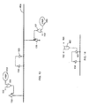
- FIG. 1a shows an embodiment of simple implementation of the principles according to the present invention.
- a memory sub-system contains two memory banks 101 and 102.
- memory bank means a memory block containing either multiple banks or towers organized in one or more data bytes or a single memory organized in multiple bytes.
- the memory sub-system can be either cache memory or standard memory.
- the memory banks 101 and 102 are addressed and selected by a memory address and select unit 9.
- Each memory bank outputs 16 bit data at its respective data input/output port.
- the output ports are coupled with the input of 2x16 multiplexers 401, 402, respectively.
- Each multiplexer 401 and 402 comprises two 16 bit outputs which are coupled with 16 bit sub-busses 410 and 420.
- a register file 8 is provided which contains a plurality of 16 bit registers 81, 82, 83, 84, ... Register file 8 is organized in a way, that two registers are accessible in parallel. Register file 8 is coupled with both 16 bit sub-busses 410 and 420.
- Fig. 1b is functional identical to Fig. 1a.
- the multiplexers 401 and 402 are placed between the sub-busses 410, 420 and the register file 8.
- the multiplexers are controlled by memory address and select unit 9.
- Both arrangements are capable of transferring two 16 bit words from or to register file 8 to or from memory sub-system 1 in parallel.
- the register file is organized in such a way that two registers are accessible at the same time, for example, register 81 and register 82 or register 83 and register 84, etc.
- the multiplexers can perform an alignment in case data to be transferred to the register file 8 is not aligned with memory bank 101. This will be explained in more detail below. Both arrangements can also transfer a single word (16 bit) from one of the two memory banks 101, 102 to any register in the register file 8.
- Additional multiplexers in the register file can provide transfer of single bytes in this arrangement.
- the whole embodiment can be expanded to a 8 bit sub-bus system using four 8 bit sub-busses and respective multiplexers.
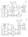
- Fig. 2 shows a block diagram of an interface 4 between a register file 8 and a memory subsystem 1 in a microcontroller or microprocessor.
- the memory sub-system 1 comprises 4 memory banks 101, 102, 103, and 104. Each memory bank is organized in 16 bits. In other words, each memory bank has a 16-bit data input/output port.
- a memory address and select unit 9 is provided to select each memory bank individually. Unit 9 also provides the addressing of the memory banks which is usually common for all banks but can be provided individually at least in part as will be explained later.
- the interface 4 comprises a bus having four 16-bit sub-busses 410, 420, 430, and 440.
- Each bus 410, 420, 430, and 440 is bi-directional and connected to bi-directional input/output ports of four multiplexers 401, 402, 403, and 404, respectively.
- Each multiplexer 401, 402, 403, and 404 couples one of the four sub-busses 410, 420, 430, and 440 with the input/output pod of an appropriate memory bank 101, 102, 103, or 104.
- Register file 8 comprises two banks of registers 810, 820 each having a number of registers. Each register has 32 bits and comprises an upper 16 bit portion 801 and a lower 16 bit portion 802.
- the upper portion 801 of register bank 810 is coupled with sub-bus 410, the lower portion 802 with sub-bus 420, the upper portion 803 of register bank 820 with sub-bus 430, and the lower portion of register bank 820 with sub-bus 440.
- control logic for selecting the sub-busses 410, 420, 430, and 440 and the multiplexers 401, 402, 403, and 404, etc. is not shown in Fig. 2.
- the embodiment according to Fig. 2 provides the feature of reading and writing of up to two 32 bit long words or four 16 bit words in parallel from or to the memory sub-system 1.
- the register file has to be organized in a way that two or more registers are accessible in parallel.
- memory address and select unit 9 addresses the memory banks 101, 102, 103, and 104. If the data from memory 1 are aligned, then multiplexer 401 selects sub-bus 410, multiplexer 402 selects sub-bus 420, multiplexer 403 selects sub-bus 430, and multiplexer 404 selects sub-bus 440.
- the register select unit (not shown) select one register in each register bank 810, 820.
- the same register in each bank 810 and 820 are addressed.
- two 32 bit long words will be written into the register file in a single cycle. If the data stored in the memory is not aligned, for example, if the two 32 bit long words start in memory bank 102 at address X, followed by the data in banks 103, and 104 at the same address and ending with data stored in memory bank 101 at the address X+8 (with byte-wise addressing), then memory address and select unit addresses memory banks 102, 103, 104 with address X and memory bank 1 with address X+8.
- the respective outputs are coupled with the register file 8 as follows: Multiplexer 401 couples memory bank 101 with sub-bus 440, multiplexer 402 couples memory bank 102 with sub-bus 410, multiplexer 403 couples memory bank 103 with sub-bus 420, and multiplexer 404 couples memory bank 104 with sub-bus 430.
- the interface 4 automatically aligns it for reading or writing in or out of register file 8.
- This scheme is shown for 16 bit words as the smallest data which can be loaded or stored. Nevertheless, the scheme can be easily adapted to higher or lower data structures, such as 8 bit data or 32 bit data, etc.
- the arrangement according to Fig. 2 can also be used to store or load a single 16 bit word from or to memory 1. For example if a 16 bit word is to loaded from memory bank 3 into a upper portion register in register bank 810, then memory address and select unit 9 selects and addresses memory bank 103.
- the data from the output port of memory bank 3 is coupled with sub-bus 410 through multiplexer 403.
- the register select logic (not shown) select the proper register out of register bank 810, for example register portion 801.
- Fig. 2 shows the multiplexers or switches between the memory sub-system 1 and the busses 410, 420, 430, and 440.
- the multiplexers or switches can be placed between the busses 410, 420, 430, and 440 and the register file 8.
- the switches can be on both sides. This is dependent on the implementation and layout of the respective microprocessor or microcontroller.
- Fig. 3 shows an embodiment which is expanded in view of the embodiment shown in Fig. 2.
- the arrangement of Fig. 2 is simply doubled. Therefore, two memory blocks are provided within memory sub-system 1.
- Each memory block contains 4 memory banks 101, 102, 103, 104, 101', 102', 103', and 104'.
- the embodiment also comprises two buses 4 and 4' and respective multiplexers 401, 402, 403, 404, 401', 402', 403', and 404'.
- two separate register files 8 and 8' are provided.
- register file 8 can be a address register file and register file 8' a data register file.
- the transfer of data into the registers takes place in the same manner as described above.
- Memory subsystem 1 is divided into two separate memory blocks wherein address register file 8 has access only to memory banks 101, 102, 103, and 104 whereas register file 8' has only access to memory banks 101', 102', 103', and 104'. In many application this is not disadvantageous as the central processing unit provides means to transfer data from register file 8 to register file 8' and vice versa.
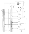
- FIG. 4 shows a third embodiment according to the present invention.
- a memory block 1 is coupled by a 64 bit read bus 1a and a 64 bit write bus 1b with a coupling unit 42 of a first 64 bit bus 46.
- a single bi-directional bus can be used.
- the two memory banks can be addressed with either a common address signal generated by a memory address and select unit (not shown) or an individual address signal for each memory bank generated by the memory address and select unit.
- memory address and select unit provides a address incrementer as will be explained later.
- a second coupling unit 44 couples bus 46 with respective 64 bit read and write buses of an address register file 8.
- a ' indicates the same elements on the data register file side.
- Interface 4 comprises a second bus 47 with coupling units 43 and 45. Between the two busses 46 and 47 a bridge is provided, this bridge 41 is controllable and can couple both busses 46 and 47.
- a switch control unit 3 is provided which controls the coupling units 42, 43, 44, and 45, the bridge 41 and an external interface 7 which can couple external devices through busses 7a, 7b, and 7c.
- Fig. 4 shows basically the same elements as Fig. 3.
- a bridge unit 41 is provided, if this bridge unit 41 is activated by switch control 3, then only up to 2 32 bit long words or 4 16 bit words can be transferred to or from either address register file 8 or data register file 8'.
- memory block 1 or memory block 1' can be source or destination in this mode.
- both memory blocks 1 and 1' can form a single memory with consecutive memory addresses and data can be transferred from any location within this memory to any register in the register files 8 and 8'.
- the external interface 7 can provide data which can be transferred to either register file.
- an additional internal interface (not shown), for example, coupled with bus 46 or 47, can be provided to transfer data from or to other on-chip devices.
- Bridge 41 thereby selects the way the data is routed which can be from or to either internal memory bank 1, 1' to or from the register files 8, 8', the external interface 7 or internal interface.
- the bridge 41 allows a plurality of combinations.
- the bridge 41 is deactivated then the content of two 32 bit registers in the address register file and of two 32 bit registers in the data register file can be transferred within one single cycle from or to the memory subsystem 1, 1'. This is very advantageous in case of a context switch where depending upon implementation the content of a number of registers has to be stored and restored. For example, if a context consists of four data and four address registers a context switch with an embodiment according to Fig. 4 takes only 2 cycles for storing and two cycles for restoring the respective registers.
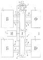
- Fig. 5 shows an embodiment of one side of interface 4 including, for example, coupling units 42, bus 46, and coupling unit 44.
- Memory block 1 is divided into four memory towers or banks 101, 102, 103, and 104.
- Bus 46 is divided into four 16 bit sub-busses 46a, 46b, 46c, and 46d.
- Each memory tower has a 16 bit data input/output pod 101a, 102a, 103a, and 104a.
- Port 101a is coupled with sub-bus 46b and sub-bus 46d.
- Port 102a is coupled with sub-bus 46a and sub-bus 46c.
- Port 103a is coupled with sub-bus 46b and sub-bus 46d.
- Port 104a is coupled with sub-bus 46a and sub-bus 46c.
- Coupling bus 801 is coupled with sub-bus 46a and 46b.
- Coupling bus 802 is coupled with sub-bus 46b and 46c.
- Coupling bus 803 is coupled with sub-bus 46c and 46d.
- Coupling bus 804 is coupled with sub-bus 46d and 46a.
- Each dot in Fig. 5 indicates a coupling of each of the 16 lines of a port or coupling bus with one of the 16 respective lines of the sub-bus.
- a first tri-state driver 48 is connected with one line of an input/output port of memory sub-system 1.
- a second tri-state driver 49 is provided. Its input is connected to the same line of bus 46 and its output is connected with the same port of memory subsystem 1.
- This embodiment shows bi-directional busses. Of course, unidirectional busses can be used as well.
- Memory 1 comprises even and odd memory towers each having a port.
- the register file 8 comprises a plurality of registers, whereby a number of registers are accessible in parallel.
- the register file has a bit width which is at least equal to the sum of the bit width of each memory tower port, for example, if four memory towers each having a 16 bit port are used, then the register file 8 comprises at least two 32 bit registers or four 16 bit registers being accessible in parallel.
- the register file interface forms a multiple n-bit interface to said register file.
- the coupling bus comprises even and odd sub-busses, whereby first couplers are bi-directional tri-state drivers coupling each odd memory tower with each even sub-bus and each even memory tower with each even sub-bus and whereby the second couplers couple the sub-busses with the register file interface in such a way, that said port of any memory tower can be coupled with any n-bit part of said register file interface.
- each memory tower 101, 102, 103, 104 could be selectively coupled with each sub-bus and each coupling bus 801, 802, 803, and 804 would be fixedly coupled with one of the sub-busses 46a, 46b, 46c, 46d, respectively.
- a further embodiment would provide all selective couplings between coupling busses 801, 802, 803, 804 and the sub-busses 46a, 46b, 46c, 46d and fixed connections between the memory towers 101, 102, 103, 104 and the sub-busses 46a, 46b, 46c, 46d.
- Port 103a is coupled sub-bus 46b
- port 104a is coupled with sub-bus 46c
- port 101a is coupled with sub-bus 46d
- port 102a is coupled with sub-bus 46a.
- sub-bus 46b is coupled with coupling bus 801
- sub-bus 46c is coupled with coupling bus 802
- sub-bus 46d is coupled with coupling bus 803
- sub-bus 46a is coupled with coupling bus 804.
- Fig. 6 shows an access scheme which allows access of unaligned data in a memory block with a plurality of memory banks within a single cycle.
- Fig. 6 are again 4 memory banks 101. 102, 103, and 104 with respective input/output ports 101a, 102a, 103a, and 104a shown.
- Each bank is addressed by address and select unit 9 by the upper address bit lines 90 which form the main address part of a respective address which addresses a 32 bit data portion of each bank 101, 102, 103, and 104.
- the 32 bit data portion consists of two 16 bit memory cells 101b, 101c in memory bank 101, 102b, 102c in memory bank 102, 103b, 103c in memory bank 103, and 104b, 104c in memory bank 104.
- Data in memory block 1 are stored in a sequential order such that memory cells 101b 102b, 103b, 104b, 101c, 102c, 103c, 104c, etc. form consecutive memory cells within memory block 1.
- memory cells 101b, 102b, 103b, and 104b contain the upper data part and memory cells 101c, 102c, 103c, and 104c contain the lower data part of a 128 bit data word.
- Special address bit lines 91, 92, 93, 94 are used to select individually upper or lower memory cells in each bank 101, 102, 103, and 104. For example, as shown in Fig. 6, if unaligned 64 bit data start in memory bank 102 and end in memory bank 101 indicated by the shaded memory cells 102b, 103b, 104b, and 101c. Address and select unit 9 selects these memory cells through address lines 90, 91, 92, 93, and 94. Ports 101a, 102a, 103a, and 104a then carry the unaligned 64 bit data word which will be aligned through interface 4 as described above.
- Fig. 7 shows a second embodiment of memory block 1.
- two memory banks 105 and 106 are provided. Each memory bank is organized in 64 bits.
- Bank 105 contains the "upper/lower” data and is addresses by address lines 95 through memory address and select unit 9 to output 64 bit in parallel.
- Bank 106 contains the "lower/upper” data and is addressed by address lines 96 through unit 9 to output also 64 bit in parallel.
- Address lines 95 and 96 can be partly identical, for example only the least significant bit is handled differently. Depending on this least significant bit it is decided whether bank 105 or 106 contains the upper or lower part.
- Memory address and select unit 9 provides an address incrementer to allow different addresses on address lines 95 and 96.
- the 64 bit output is fed in four 16 bit portions to four 2x16 multiplexers 107, 108, 109, and 110.
- the outputs of each multiplexer 101a, 102a, 103a and 104a carry the unaligned 64 bit data from memory 1.
- the multiplexers are controlled by memory address and select unit 9.
- the memory banks 105 and 106 are organized in such a way, that data start in the first row of bank 105, continue in the first row of bank 106, followed by row 2 of bank 105 and so on. Again, for example, if unaligned 64 bit data start with the third 16 bit portion in memory bank 105, as indicated by the shadowed memory cells in Fig. 7, unit 9 selects the same memory lines in bank 105 and 106.
- multiplexers 107, 108, 109, and 110 the respective 16 bit portions of bank 105 or bank 106 are selected and fed to output ports 101a, 102a, 103a, and 104a.
- multiplexers 109 and 110 select bank 105 and multiplexers 107 and 108 select bank 106.
- the actual alignment is done by interface 4 as described above.
- address lines 95 and 96 must provide select lines for each memory cell within a row of memory banks 105 and 106.
- Fig. 8 shows an embodiment of the bridge unit 41 shown in Fig. 4.
- Bus 46 and 47 each are divided into four 16 bit sub-busses.
- Each line of each sub-bus of bus 46 is coupled with the respective line of bus 47 by means of two tri-state drivers.
- Fig. 8 shows only drivers for one of sixteen lines for each sub-bus.
- the tri-state driver pairs 450, 451; 460, 461; 470, 471; 480, 481 each form a selectable bi-directional coupling element.
- Each driver either functions as a read or write driver depending on the source and destination of the respective data.
- the upper or lower drivers of each line can be enabled commonly or separately for each 16 bit sub-bus.
- top drivers 450, 460, 470, and 480 are enabled by a single signal and all bottom drivers 451, 461, 471, and 481 are enabled by a second signal.
- FIG. 9 Another embodiment of the memory interface is shown in Fig. 9.
- a single memory block 120 is provided.
- This memory block 120 is organized in 128 bits.
- the interface between register file and memory consists of 32 double 2x1 multiplexers M1 - M32 as primary switches, an intermittent bus 490 and 8 barrel shifters as secondary switches.
- Each multiplexer M1-M32 contains two 2x1 multiplexers.
- the multiplexers M1-M32 are individually controlled by control signal C.
- Each bit cell output of an addressed row of memory block 120 is coupled with an input of a multiplexer M1-M32.
- 4 multiplexers M1-M4; M5-M8;.... M29-M32 respectively are coupled with one of 8 barrel shifters B1-B8.
- the barrel shifters are controlled by signal B.
- the barrel shifters B1-B8 output 64 bits in parallel which are fed to the register file.
- the 128 bits of each row of memory block 120 are not stored in a consecutive order.
- the bit order starts with bit D0, D8, D64, D72, D16, D24, D80, D88,...D48, D56, D112, D120,...D55, D63, D119, D127.
- the order is divided into eight blocks each having four 4 bit groups.
- the multiplexers M1-M8 select two data lines out of a 4 bit group, whereby either the first two and or the second two bits are selected, for example, multiplexer M1 selects either data pair D0, D8 or data pair D64, D72.
- the multiplexers M1-M32 are controlled separately, in other words each double multiplexer M1-M32 is controlled by a different control line. Therefore, control signal C consists of at least 32 control lines.
- the output of all multiplexers form a 64 bit bus 490.
- Eight 8-Bit barrel shifters B1-B8 form the secondary switches which switch the data on the 64 bit lines of bus 490. Each barrel shifter performs a left shift in increments of two bit depending on the control signal B which is formed by respective address signals.
- Memory address and select unit (not shown) generate select signal A which selects the third row of memory 120. Thus, all 128 bits of this memory row are fed to the inputs of multiplexers M1-M32.
- a switch control unit (not shown), which may be part of memory address and select unit, selects the second data pair of multiplexers M1, M5, M9, M13, M17,...
- barrel shifter B1 receives the following data signals: D64, D72, D16, D24, D32, D40, D48, and D56.
- Signal B is common for all eight barrel shifters and indicates in this example to shift the data byte by one step. As mentioned above, one step is equal to a left shift by two bits. Therefore, the output of barrel shifter B1 carries signals D16, D24, D32,D40, D48,D56,D64,D72. Even so the output of the barrel shifters B1-B8 are not in the right order, there is a fixed relationship between each output line. Thus, no additional switching is necessary.
- the wiring selects the first bits of each barrel shifter B1-B9, followed by the second bits of each barrel shifter B1-B9, etc.
- the register file receives a data word which is the aligned 64 bit word starting with bit D16, D17, D18,...D79.
- the principle of this embodiment is to provide multiplexers as first switches which select a predefined number of bits from the data provided by the memory in parallel to the respective internal bus.
- the second switch is used to bring the extracted bits in a predefined order.
- the second switch does not necessarily reduce the number of bits but does reorder the bits so that the relation of each consecutive bit is constant.
- the order of consecutive bits stored in the memory can be arranged in many different ways and does not have to follow the order of the embodiment.
- Principle of the present invention is to interleave or scramble the bytes, words, or long words stored in memory in an appropriate manner.
- a local multiplexing can select the respective data bits.
- the write enable signal has to be also interleaved to access the respective memory cells during a write cycle.
- the write enable signal for the first byte has to go to bit 0,1, 2, 3,...7 which are not in consecutive order.
- the barrel shifter can of course be realized by multiplexers or in any other known way.
- the output bit lines of barrel shifters B1-B8 do not have to be ordered before they are coupled with the register file. Depending on the size of each register this can also be done between the register file and the execution units as only execution units which actually manipulate the content of a register need the content of a data byte or word in order. Nevertheless, in a 32 bit microcomputer with 32 bit registers where a register might store 4 bytes, 2 words or 1 long word, it is advantageous to order the bits fed from the interface to the register file.
- any conventional memory externally or internally, can be used as the bit order in the memory is of no concern as long reading and writing lines use the same order. Thus, in case of a dual port memory with different port orders, a rewiring on either port has to be performed to ensure proper order of the memory content.
- Fig. 10 shows a data transfer using the embodiment of Fig.4. Both memory banks are addressed by the same address signal generated by memory address and select unit 9. Each memory bank has a four 16 Bit - word wide interface, for example 64 bits. Bus 46 and bus 47 each consist of four 16 Bit wide sub-busses 46a, 46b, 46c, 46d and 47a, 47b, 47c, 47d, respectively. If all four 16 Bit words are to be transferred from one memory bank to one of the register files 8, 8' the transfer takes place with or without usage of bridge 41. In case of a boundary crossing data from both memory banks have to be transferred into one register file. This scenario is shown in Fig. 10.
- the first two 16 Bit words are stored at the last two memory positions of the first memory bank 1 and the following two 16 Bit words are stored within the second memory bank 1'.
- the content of the last two memory cells of the first memory bank are transferred on sub-bus 46a and 46b.
- Bridge 41 couples sub-bus 46a with 47a and sub-bus 46b with 47b.
- the second two 16 Bit words are transferred from the first two memory cells within the second memory bank 1' onto sub-bus 47c and 47d, respectively. Through coupling bus 8a' the four 16 Bit words are transferred into register file 8'.
- Fig. 11 depicts a second scenario in which a crossing from the second memory bank 1' to the first memory bank 1 takes place.
- memory address and select unit 9 has to provide different addresses for each memory bank. Therefore, memory address and select unit 9 comprises an address incrementer to increment an address provided, for example, to memory bank 1' for memory bank 1. It for example, four 16 Bit words are stored within the memory under an address, that, for example, the first 16 Bit word is stored in the last memory cell in one row of the second memory bank 1', then the succeeding memory cells are located under a succeeding address in the first memory bank 1.
- the incrementer increments the address, in this example by 64, and provides the first memory bank 1 with the incremented address.
- the content of the last memory cell of the addressed row in the second memory bank 1' is transferred on sub-busses 47a.
- the content of the first three memory cells of the row of the first memory bank 1 addressed by the incremented address are transferred to sub-busses 46b, 46c, and 46d, through the bridge to sub-busses 47b, 47c and 47d.
- the transfer to register file 8' takes place in the same manner as described above.
- Fig. 12 depicts a third scenario in which, for example, a context switch takes place.
- the purpose of such a transfer is to load or store the content of a context represented by the content of a plurality of registers as quickly as possible.
- the bridge 41 completely de-couples busses 42 from busses 43.
- 64 bit from memory bank 1 can be transferred to register file 8 in parallel with 64 bits from memory bank 1' to register file 8' or vice versa. Therefore, memory address and select unit 9 addresses both memory banks 1 and 1' with usually the same address were the context content is stored or is to be stored to. External or internal interfaces are usually also de-coupled during such a process.
- Figs. 10, 11, and 12 do not show the couplers 42, 43, 44, and 45 according to Fig. 4. for a better overview, only the different data paths are shown.
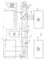
- Fig.13 shows an embodiment of a single bus line, for example, bus line 46a.
- Transfer from memory or register file to the busline 46a is established via two tristate inverters 150 and 156.
- a simple logic consisting of NOR gate 151 and 157 controlled by a clock signal 152 and respective logic signals 153 and 158 controls drivers 150 and 152. If the drivers 150 and 156 are not enabled a special bus holder arrangement secures the status of the bus line in a defined manner.
- the bus holder consists of a first inverter 154 whose input is coupled with bus line 46a and whose output is coupled with the input of a second inverter 155 whose output is coupled with bus line 46a.
- Inverter 155 is preferably weak to avoid a unnecessary load on the bus line for one of the drivers 150 or 156. Such an arrangement avoids congestion problems on a bus line as the bus line is only actively driven during the low phase of the clock signal 152. During the high phase of the clock signal 152 drivers 150 and 156 are disabled. Thus, an improved signal flow can be achieved.
- Fig. 14 shows an improvement of the bus holder.
- a first inverter 160 is coupled with a second inverter 161 in series to hold a signal on a bus line.
- the second inverter 161 is a strong driver but switched. This driver is only active when the clock signal 152 is high and no other driver is active. These two conditions are anded by an AND gate 162 whose output controls driver 161.
Landscapes
- Engineering & Computer Science (AREA)
- Theoretical Computer Science (AREA)
- Physics & Mathematics (AREA)
- General Engineering & Computer Science (AREA)
- General Physics & Mathematics (AREA)
- Executing Machine-Instructions (AREA)
- Memory System (AREA)
Applications Claiming Priority (2)
| Application Number | Priority Date | Filing Date | Title |
|---|---|---|---|
| US09/192,170 US6405273B1 (en) | 1998-11-13 | 1998-11-13 | Data processing device with memory coupling unit |
| US192170 | 2008-08-15 |
Publications (2)
| Publication Number | Publication Date |
|---|---|
| EP1001347A2 true EP1001347A2 (de) | 2000-05-17 |
| EP1001347A3 EP1001347A3 (de) | 2003-04-09 |
Family
ID=22708548
Family Applications (1)
| Application Number | Title | Priority Date | Filing Date |
|---|---|---|---|
| EP99116654A Withdrawn EP1001347A3 (de) | 1998-11-13 | 1999-08-26 | Datenverarbeitungsgerät mit Speicherkopplungseinheit |
Country Status (3)
| Country | Link |
|---|---|
| US (2) | US6405273B1 (de) |
| EP (1) | EP1001347A3 (de) |
| JP (1) | JP2000231535A (de) |
Cited By (7)
| Publication number | Priority date | Publication date | Assignee | Title |
|---|---|---|---|---|
| WO2007005891A2 (en) * | 2005-06-30 | 2007-01-11 | Intel Corporation | Micro-tile memory interfaces |
| WO2007005551A3 (en) * | 2005-06-30 | 2007-08-16 | Intel Corp | Automatic detection of micro-tile enabled memory |
| EP1866769A2 (de) * | 2005-02-23 | 2007-12-19 | Micron Technology, Inc. | Speicherbaustein und verfahren mit mehreren internen datenbussen und speicherbank-verschachtelung |
| US7765366B2 (en) | 2005-06-23 | 2010-07-27 | Intel Corporation | Memory micro-tiling |
| US8253751B2 (en) | 2005-06-30 | 2012-08-28 | Intel Corporation | Memory controller interface for micro-tiled memory access |
| US8332598B2 (en) | 2005-06-23 | 2012-12-11 | Intel Corporation | Memory micro-tiling request reordering |
| US8878860B2 (en) | 2006-12-28 | 2014-11-04 | Intel Corporation | Accessing memory using multi-tiling |
Families Citing this family (29)
| Publication number | Priority date | Publication date | Assignee | Title |
|---|---|---|---|---|
| US6823016B1 (en) * | 1998-02-20 | 2004-11-23 | Intel Corporation | Method and system for data management in a video decoder |
| US6405273B1 (en) * | 1998-11-13 | 2002-06-11 | Infineon Technologies North America Corp. | Data processing device with memory coupling unit |
| US6633576B1 (en) * | 1999-11-04 | 2003-10-14 | William Melaragni | Apparatus and method for interleaved packet storage |
| US6732203B2 (en) * | 2000-01-31 | 2004-05-04 | Intel Corporation | Selectively multiplexing memory coupling global bus data bits to narrower functional unit coupling local bus |
| US6769046B2 (en) * | 2000-02-14 | 2004-07-27 | Palmchip Corporation | System-resource router |
| US6721295B1 (en) * | 2000-08-25 | 2004-04-13 | Texas Instruments Incorporated | Triple data system for high data rate communication systems |
| US6584537B1 (en) * | 2000-12-06 | 2003-06-24 | Lsi Logic Corporation | Data-cache data-path |
| JP2002215606A (ja) * | 2001-01-24 | 2002-08-02 | Mitsubishi Electric Corp | データ処理装置 |
| US20040078608A1 (en) * | 2001-04-02 | 2004-04-22 | Ruban Kanapathippillai | Method and apparatus for power reduction in a digital signal processor integrated circuit |
| FI20011257A0 (fi) * | 2001-06-13 | 2001-06-13 | Nokia Corp | Menetelmä väylän mukauttamiseksi ja väylä |
| JP4325130B2 (ja) * | 2001-06-21 | 2009-09-02 | ヤマハ株式会社 | 電子機器 |
| US7146454B1 (en) * | 2002-04-16 | 2006-12-05 | Cypress Semiconductor Corporation | Hiding refresh in 1T-SRAM architecture |
| US8005212B2 (en) * | 2002-07-10 | 2011-08-23 | Infineon Technologies Ag | Device and method for performing a cryptoalgorithm |
| US7836252B2 (en) | 2002-08-29 | 2010-11-16 | Micron Technology, Inc. | System and method for optimizing interconnections of memory devices in a multichip module |
| US7245145B2 (en) | 2003-06-11 | 2007-07-17 | Micron Technology, Inc. | Memory module and method having improved signal routing topology |
| US7120743B2 (en) | 2003-10-20 | 2006-10-10 | Micron Technology, Inc. | Arbitration system and method for memory responses in a hub-based memory system |
| US7366864B2 (en) | 2004-03-08 | 2008-04-29 | Micron Technology, Inc. | Memory hub architecture having programmable lane widths |
| US7120723B2 (en) * | 2004-03-25 | 2006-10-10 | Micron Technology, Inc. | System and method for memory hub-based expansion bus |
| US7590797B2 (en) | 2004-04-08 | 2009-09-15 | Micron Technology, Inc. | System and method for optimizing interconnections of components in a multichip memory module |
| US7398347B1 (en) * | 2004-07-14 | 2008-07-08 | Altera Corporation | Methods and apparatus for dynamic instruction controlled reconfigurable register file |
| US7392331B2 (en) * | 2004-08-31 | 2008-06-24 | Micron Technology, Inc. | System and method for transmitting data packets in a computer system having a memory hub architecture |
| US7747833B2 (en) * | 2005-09-30 | 2010-06-29 | Mosaid Technologies Incorporated | Independent link and bank selection |
| JP5204777B2 (ja) * | 2007-12-21 | 2013-06-05 | パナソニック株式会社 | メモリ装置及びその制御方法 |
| US20130297858A1 (en) * | 2012-04-19 | 2013-11-07 | Stec, Inc. | Systems and methods for providing channel buffer in a solid-state device |
| WO2014073188A1 (ja) * | 2012-11-08 | 2014-05-15 | パナソニック株式会社 | 半導体回路のバスシステム |
| CN104699219B (zh) * | 2013-12-10 | 2020-06-23 | 联想(北京)有限公司 | 一种电子设备及信息处理方法 |
| US9774317B1 (en) * | 2016-08-29 | 2017-09-26 | Amazon Technologies, Inc. | Bistable-element for random number generation |
| US20190347219A1 (en) * | 2018-05-09 | 2019-11-14 | Micron Technology, Inc. | Memory devices having a reduced global data path footprint and associated systems and methods |
| US10747693B2 (en) * | 2018-05-10 | 2020-08-18 | Micron Technology, Inc. | Semiconductor device with a time multiplexing mechanism for size efficiency |
Citations (3)
| Publication number | Priority date | Publication date | Assignee | Title |
|---|---|---|---|---|
| US5226142A (en) * | 1990-11-21 | 1993-07-06 | Ross Technology, Inc. | High performance register file with overlapping windows |
| US5481734A (en) * | 1989-12-16 | 1996-01-02 | Mitsubishi Denki Kabushiki Kaisha | Data processor having 2n bits width data bus for context switching function |
| JPH086760A (ja) * | 1994-06-20 | 1996-01-12 | Hitachi Ltd | データ処理装置 |
Family Cites Families (7)
| Publication number | Priority date | Publication date | Assignee | Title |
|---|---|---|---|---|
| US5307506A (en) * | 1987-04-20 | 1994-04-26 | Digital Equipment Corporation | High bandwidth multiple computer bus apparatus |
| WO1994003860A1 (en) * | 1992-08-07 | 1994-02-17 | Thinking Machines Corporation | Massively parallel computer including auxiliary vector processor |
| US5787488A (en) * | 1993-04-22 | 1998-07-28 | Analog Devices, Inc. | Multi-phase multi-access pipeline memory system |
| US5875470A (en) * | 1995-09-28 | 1999-02-23 | International Business Machines Corporation | Multi-port multiple-simultaneous-access DRAM chip |
| US5954811A (en) * | 1996-01-25 | 1999-09-21 | Analog Devices, Inc. | Digital signal processor architecture |
| US6343356B1 (en) * | 1998-10-09 | 2002-01-29 | Bops, Inc. | Methods and apparatus for dynamic instruction controlled reconfiguration register file with extended precision |
| US6405273B1 (en) * | 1998-11-13 | 2002-06-11 | Infineon Technologies North America Corp. | Data processing device with memory coupling unit |
-
1998
- 1998-11-13 US US09/192,170 patent/US6405273B1/en not_active Expired - Lifetime
-
1999
- 1999-08-26 EP EP99116654A patent/EP1001347A3/de not_active Withdrawn
- 1999-11-15 JP JP11323951A patent/JP2000231535A/ja active Pending
-
2002
- 2002-05-08 US US10/141,996 patent/US20020129188A1/en not_active Abandoned
Patent Citations (3)
| Publication number | Priority date | Publication date | Assignee | Title |
|---|---|---|---|---|
| US5481734A (en) * | 1989-12-16 | 1996-01-02 | Mitsubishi Denki Kabushiki Kaisha | Data processor having 2n bits width data bus for context switching function |
| US5226142A (en) * | 1990-11-21 | 1993-07-06 | Ross Technology, Inc. | High performance register file with overlapping windows |
| JPH086760A (ja) * | 1994-06-20 | 1996-01-12 | Hitachi Ltd | データ処理装置 |
Non-Patent Citations (1)
| Title |
|---|
| PATENT ABSTRACTS OF JAPAN vol. 1996, no. 05, 31 May 1996 (1996-05-31) & JP 08 006760 A (HITACHI LTD), 12 January 1996 (1996-01-12) * |
Cited By (18)
| Publication number | Priority date | Publication date | Assignee | Title |
|---|---|---|---|---|
| EP1866769A4 (de) * | 2005-02-23 | 2011-11-02 | Micron Technology Inc | Speicherbaustein und verfahren mit mehreren internen datenbussen und speicherbank-verschachtelung |
| EP1866769A2 (de) * | 2005-02-23 | 2007-12-19 | Micron Technology, Inc. | Speicherbaustein und verfahren mit mehreren internen datenbussen und speicherbank-verschachtelung |
| US7765366B2 (en) | 2005-06-23 | 2010-07-27 | Intel Corporation | Memory micro-tiling |
| US8332598B2 (en) | 2005-06-23 | 2012-12-11 | Intel Corporation | Memory micro-tiling request reordering |
| US8010754B2 (en) | 2005-06-23 | 2011-08-30 | Intel Corporation | Memory micro-tiling |
| EP2006775A2 (de) * | 2005-06-30 | 2008-12-24 | Intel Corporation | Mikro-Tile-Speicherschnittstelle |
| EP2006775A3 (de) * | 2005-06-30 | 2009-01-14 | Intel Corporation | Mikro-Tile-Speicherschnittstelle |
| US7558941B2 (en) | 2005-06-30 | 2009-07-07 | Intel Corporation | Automatic detection of micro-tile enabled memory |
| EP2006858A3 (de) * | 2005-06-30 | 2009-01-14 | Intel Corporation | Mikro-Tile-Speicherschnittstelle |
| WO2007005891A2 (en) * | 2005-06-30 | 2007-01-11 | Intel Corporation | Micro-tile memory interfaces |
| US8032688B2 (en) | 2005-06-30 | 2011-10-04 | Intel Corporation | Micro-tile memory interfaces |
| WO2007005551A3 (en) * | 2005-06-30 | 2007-08-16 | Intel Corp | Automatic detection of micro-tile enabled memory |
| CN1929026B (zh) * | 2005-06-30 | 2012-06-06 | 英特尔公司 | 一种存储器集成电路以及存储器阵列 |
| US8200883B2 (en) | 2005-06-30 | 2012-06-12 | Intel Corporation | Micro-tile memory interfaces |
| US8253751B2 (en) | 2005-06-30 | 2012-08-28 | Intel Corporation | Memory controller interface for micro-tiled memory access |
| WO2007005891A3 (en) * | 2005-06-30 | 2007-05-03 | Intel Corp | Micro-tile memory interfaces |
| US8866830B2 (en) | 2005-06-30 | 2014-10-21 | Intel Corporation | Memory controller interface for micro-tiled memory access |
| US8878860B2 (en) | 2006-12-28 | 2014-11-04 | Intel Corporation | Accessing memory using multi-tiling |
Also Published As
| Publication number | Publication date |
|---|---|
| EP1001347A3 (de) | 2003-04-09 |
| JP2000231535A (ja) | 2000-08-22 |
| US20020129188A1 (en) | 2002-09-12 |
| US6405273B1 (en) | 2002-06-11 |
Similar Documents
| Publication | Publication Date | Title |
|---|---|---|
| EP1001347A2 (de) | Datenverarbeitungsgerät mit Speicherkopplungseinheit | |
| EP0714534B1 (de) | Mehrfachport-verteilte speicherschnittstelle und zugehöriges verfahren | |
| US5961640A (en) | Virtual contiguous FIFO having the provision of packet-driven automatic endian conversion | |
| US6408367B2 (en) | Data path architecture and arbitration scheme for providing access to a shared system resource | |
| US5910928A (en) | Memory interface unit, shared memory switch system and associated method | |
| US4652993A (en) | Multiple output port memory storage module | |
| EP0165822B1 (de) | Speicherzugriffsteuerungsanordnung | |
| JP3099931B2 (ja) | 半導体装置 | |
| US5761478A (en) | Programmable memory interface for efficient transfer of different size data | |
| US20020166023A1 (en) | High speed bus interface for non-volatile integrated circuit memory supporting continuous transfer | |
| JPH0756815A (ja) | キャッシュ動作方法及びキャッシュ | |
| EP1381957A2 (de) | Datenverarbeitungsgerät, -system und -verfahren zur speicherzugriffssteuerung | |
| US20050180240A1 (en) | Method and system for fast memory access | |
| KR960004457B1 (ko) | 데이터 전송장치 | |
| US6041387A (en) | Apparatus for read/write-access to registers having register file architecture in a central processing unit | |
| JPH04306756A (ja) | データ転送システム | |
| US5774653A (en) | High-throughput data buffer | |
| US6401161B1 (en) | High speed bus interface for non-volatile integrated circuit memory supporting continuous transfer | |
| US20050071576A1 (en) | Data processing apparatus and system and method for controlling memory access | |
| GB2117945A (en) | Memory data transfer | |
| JPH03116350A (ja) | データ転送のバス構造 | |
| JPS617956A (ja) | メモリの多重アクセス制御方式 | |
| JPH0496189A (ja) | 単一命令型並列計算機 | |
| JPH01273126A (ja) | メモリ回路 | |
| JPH11203252A (ja) | 並列プロセッサおよびメモリ制御方法 |
Legal Events
| Date | Code | Title | Description |
|---|---|---|---|
| PUAI | Public reference made under article 153(3) epc to a published international application that has entered the european phase |
Free format text: ORIGINAL CODE: 0009012 |
|
| AK | Designated contracting states |
Kind code of ref document: A2 Designated state(s): AT BE CH CY DE DK ES FI FR GB GR IE IT LI LU MC NL PT SE |
|
| AX | Request for extension of the european patent |
Free format text: AL;LT;LV;MK;RO;SI |
|
| PUAL | Search report despatched |
Free format text: ORIGINAL CODE: 0009013 |
|
| AK | Designated contracting states |
Kind code of ref document: A3 Designated state(s): AT BE CH CY DE DK ES FI FR GB GR IE IT LI LU MC NL PT SE Designated state(s): AT BE CH CY DE DK ES FI FR GB GR IE IT LI LU MC NL PT SE |
|
| AX | Request for extension of the european patent |
Extension state: AL LT LV MK RO SI |
|
| RIC1 | Information provided on ipc code assigned before grant |
Ipc: 7G 06F 9/30 A |
|
| RAP1 | Party data changed (applicant data changed or rights of an application transferred) |
Owner name: INFINEON TECHNOLOGIES NORTH AMERICA CORP. |
|
| 17P | Request for examination filed |
Effective date: 20030719 |
|
| AKX | Designation fees paid |
Designated state(s): DE FR IT |
|
| 17Q | First examination report despatched |
Effective date: 20040422 |
|
| STAA | Information on the status of an ep patent application or granted ep patent |
Free format text: STATUS: THE APPLICATION IS DEEMED TO BE WITHDRAWN |
|
| 18D | Application deemed to be withdrawn |
Effective date: 20040903 |