US5910928A - Memory interface unit, shared memory switch system and associated method - Google Patents
Memory interface unit, shared memory switch system and associated method Download PDFInfo
- Publication number
- US5910928A US5910928A US08/998,586 US99858697A US5910928A US 5910928 A US5910928 A US 5910928A US 99858697 A US99858697 A US 99858697A US 5910928 A US5910928 A US 5910928A
- Authority
- US
- United States
- Prior art keywords
- data
- memory
- port
- buffer
- burst
- Prior art date
- Legal status (The legal status is an assumption and is not a legal conclusion. Google has not performed a legal analysis and makes no representation as to the accuracy of the status listed.)
- Expired - Lifetime
Links
- 230000015654 memory Effects 0.000 title claims abstract description 328
- 238000000034 method Methods 0.000 title claims description 10
- 239000000872 buffer Substances 0.000 claims abstract description 193
- 238000012546 transfer Methods 0.000 claims abstract description 97
- 239000011159 matrix material Substances 0.000 claims description 35
- 238000000638 solvent extraction Methods 0.000 claims 2
- 238000010586 diagram Methods 0.000 description 50
- 239000012634 fragment Substances 0.000 description 25
- 230000009977 dual effect Effects 0.000 description 12
- 238000013459 approach Methods 0.000 description 4
- 241000238876 Acari Species 0.000 description 2
- 230000000903 blocking effect Effects 0.000 description 2
- 230000003139 buffering effect Effects 0.000 description 2
- 238000012986 modification Methods 0.000 description 2
- 230000004048 modification Effects 0.000 description 2
- 230000005540 biological transmission Effects 0.000 description 1
- 238000010618 wire wrap Methods 0.000 description 1
Images


Classifications
-
- G—PHYSICS
- G06—COMPUTING; CALCULATING OR COUNTING
- G06F—ELECTRIC DIGITAL DATA PROCESSING
- G06F13/00—Interconnection of, or transfer of information or other signals between, memories, input/output devices or central processing units
- G06F13/14—Handling requests for interconnection or transfer
- G06F13/16—Handling requests for interconnection or transfer for access to memory bus
-
- H—ELECTRICITY
- H04—ELECTRIC COMMUNICATION TECHNIQUE
- H04L—TRANSMISSION OF DIGITAL INFORMATION, e.g. TELEGRAPHIC COMMUNICATION
- H04L12/00—Data switching networks
- H04L12/54—Store-and-forward switching systems
- H04L12/56—Packet switching systems
- H04L12/5601—Transfer mode dependent, e.g. ATM
-
- G—PHYSICS
- G06—COMPUTING; CALCULATING OR COUNTING
- G06F—ELECTRIC DIGITAL DATA PROCESSING
- G06F13/00—Interconnection of, or transfer of information or other signals between, memories, input/output devices or central processing units
- G06F13/14—Handling requests for interconnection or transfer
- G06F13/16—Handling requests for interconnection or transfer for access to memory bus
- G06F13/1605—Handling requests for interconnection or transfer for access to memory bus based on arbitration
- G06F13/1647—Handling requests for interconnection or transfer for access to memory bus based on arbitration with interleaved bank access
-
- G—PHYSICS
- G06—COMPUTING; CALCULATING OR COUNTING
- G06F—ELECTRIC DIGITAL DATA PROCESSING
- G06F13/00—Interconnection of, or transfer of information or other signals between, memories, input/output devices or central processing units
- G06F13/14—Handling requests for interconnection or transfer
- G06F13/16—Handling requests for interconnection or transfer for access to memory bus
- G06F13/1605—Handling requests for interconnection or transfer for access to memory bus based on arbitration
- G06F13/1652—Handling requests for interconnection or transfer for access to memory bus based on arbitration in a multiprocessor architecture
- G06F13/1657—Access to multiple memories
-
- G—PHYSICS
- G06—COMPUTING; CALCULATING OR COUNTING
- G06F—ELECTRIC DIGITAL DATA PROCESSING
- G06F13/00—Interconnection of, or transfer of information or other signals between, memories, input/output devices or central processing units
- G06F13/14—Handling requests for interconnection or transfer
- G06F13/16—Handling requests for interconnection or transfer for access to memory bus
- G06F13/1605—Handling requests for interconnection or transfer for access to memory bus based on arbitration
- G06F13/1652—Handling requests for interconnection or transfer for access to memory bus based on arbitration in a multiprocessor architecture
- G06F13/1663—Access to shared memory
-
- H—ELECTRICITY
- H04—ELECTRIC COMMUNICATION TECHNIQUE
- H04L—TRANSMISSION OF DIGITAL INFORMATION, e.g. TELEGRAPHIC COMMUNICATION
- H04L49/00—Packet switching elements
- H04L49/10—Packet switching elements characterised by the switching fabric construction
- H04L49/103—Packet switching elements characterised by the switching fabric construction using a shared central buffer; using a shared memory
-
- H—ELECTRICITY
- H04—ELECTRIC COMMUNICATION TECHNIQUE
- H04L—TRANSMISSION OF DIGITAL INFORMATION, e.g. TELEGRAPHIC COMMUNICATION
- H04L49/00—Packet switching elements
- H04L49/10—Packet switching elements characterised by the switching fabric construction
- H04L49/104—Asynchronous transfer mode [ATM] switching fabrics
- H04L49/105—ATM switching elements
- H04L49/108—ATM switching elements using shared central buffer
-
- H—ELECTRICITY
- H04—ELECTRIC COMMUNICATION TECHNIQUE
- H04L—TRANSMISSION OF DIGITAL INFORMATION, e.g. TELEGRAPHIC COMMUNICATION
- H04L49/00—Packet switching elements
- H04L49/15—Interconnection of switching modules
- H04L49/1553—Interconnection of ATM switching modules, e.g. ATM switching fabrics
- H04L49/1576—Crossbar or matrix
-
- H—ELECTRICITY
- H04—ELECTRIC COMMUNICATION TECHNIQUE
- H04L—TRANSMISSION OF DIGITAL INFORMATION, e.g. TELEGRAPHIC COMMUNICATION
- H04L49/00—Packet switching elements
- H04L49/30—Peripheral units, e.g. input or output ports
- H04L49/3081—ATM peripheral units, e.g. policing, insertion or extraction
-
- H—ELECTRICITY
- H04—ELECTRIC COMMUNICATION TECHNIQUE
- H04L—TRANSMISSION OF DIGITAL INFORMATION, e.g. TELEGRAPHIC COMMUNICATION
- H04L49/00—Packet switching elements
- H04L49/60—Software-defined switches
- H04L49/606—Hybrid ATM switches, e.g. ATM&STM, ATM&Frame Relay or ATM&IP
-
- H—ELECTRICITY
- H04—ELECTRIC COMMUNICATION TECHNIQUE
- H04L—TRANSMISSION OF DIGITAL INFORMATION, e.g. TELEGRAPHIC COMMUNICATION
- H04L12/00—Data switching networks
- H04L12/54—Store-and-forward switching systems
- H04L12/56—Packet switching systems
- H04L12/5601—Transfer mode dependent, e.g. ATM
- H04L2012/5678—Traffic aspects, e.g. arbitration, load balancing, smoothing, buffer management
- H04L2012/5679—Arbitration or scheduling
-
- H—ELECTRICITY
- H04—ELECTRIC COMMUNICATION TECHNIQUE
- H04L—TRANSMISSION OF DIGITAL INFORMATION, e.g. TELEGRAPHIC COMMUNICATION
- H04L12/00—Data switching networks
- H04L12/54—Store-and-forward switching systems
- H04L12/56—Packet switching systems
- H04L12/5601—Transfer mode dependent, e.g. ATM
- H04L2012/5678—Traffic aspects, e.g. arbitration, load balancing, smoothing, buffer management
- H04L2012/5681—Buffer or queue management
-
- H—ELECTRICITY
- H04—ELECTRIC COMMUNICATION TECHNIQUE
- H04L—TRANSMISSION OF DIGITAL INFORMATION, e.g. TELEGRAPHIC COMMUNICATION
- H04L49/00—Packet switching elements
- H04L49/10—Packet switching elements characterised by the switching fabric construction
- H04L49/101—Packet switching elements characterised by the switching fabric construction using crossbar or matrix
-
- H—ELECTRICITY
- H04—ELECTRIC COMMUNICATION TECHNIQUE
- H04L—TRANSMISSION OF DIGITAL INFORMATION, e.g. TELEGRAPHIC COMMUNICATION
- H04L49/00—Packet switching elements
- H04L49/25—Routing or path finding in a switch fabric
- H04L49/253—Routing or path finding in a switch fabric using establishment or release of connections between ports
- H04L49/254—Centralised controller, i.e. arbitration or scheduling
-
- H—ELECTRICITY
- H04—ELECTRIC COMMUNICATION TECHNIQUE
- H04L—TRANSMISSION OF DIGITAL INFORMATION, e.g. TELEGRAPHIC COMMUNICATION
- H04L49/00—Packet switching elements
- H04L49/30—Peripheral units, e.g. input or output ports
- H04L49/3018—Input queuing
-
- H—ELECTRICITY
- H04—ELECTRIC COMMUNICATION TECHNIQUE
- H04L—TRANSMISSION OF DIGITAL INFORMATION, e.g. TELEGRAPHIC COMMUNICATION
- H04L49/00—Packet switching elements
- H04L49/35—Switches specially adapted for specific applications
- H04L49/351—Switches specially adapted for specific applications for local area network [LAN], e.g. Ethernet switches
-
- H—ELECTRICITY
- H04—ELECTRIC COMMUNICATION TECHNIQUE
- H04L—TRANSMISSION OF DIGITAL INFORMATION, e.g. TELEGRAPHIC COMMUNICATION
- H04L49/00—Packet switching elements
- H04L49/40—Constructional details, e.g. power supply, mechanical construction or backplane
Definitions
- the invention relates generally to memory interface systems, and more specifically to a method and apparatus for providing and arbitrating access to a shared memory by multiple devices, for applications such as multiprocessor systems and communications switching.
- Shared memories are used to facilitate data passing between multiple processes.
- a typical shared memory implementation involves the use of multiple ports. Each port may provide shared memory access to a different external device. The different devices, in turn, may be involved with the control or execution of different processes that pass the data.
- the path to the shared memory typically is designed with a bandwidth close to the sum of the bandwidths of the individual ports. This ensures that the data carrying capacity of the path is sufficiently large so that no port suffers a significant delay in accessing the shared memory even though multiple ports may seek access to the shared memory. Generally, this is achieved in one of two ways, or some combination thereof First, the shared memory access time may be designed to be much faster than the data transfer times for the individual ports. Second, the path width to the shared memory may be designed to be much greater than the path widths of the individual ports.
- the first approach is to assign a time slot to each port during which data can be read from or written to the shared memory.
- the assigned time slot is shorter than the actual time required to transfer data through the port.
- the data is buffered temporarily during its transfer between a port and the shared memory.
- the length of the port time slot is inversely proportional to the number of devices sharing access to the shared memory.
- a device using a particular port can gain access to the memory only during the assigned time slot for that port.
- Data is buffered between time slots.
- the second approach also involves assigning a time slot to each port. For example, writes to the shared memory involve temporarily buffering multiple data words received at a respective port, and then providing them to the memory on a wide memory path all in one memory access cycle during the time slot designated for the port. Conversely, reads from the shared memory involve providing multiple words on the wide path all in one memory access cycle during a time slot designated for a respective port; temporarily buffering the words read from memory; and then transferring the words through the port.
- This second approach is particularly well suited to burst-mode systems in which data words are communicated in multi-word bursts through respective ports.
- a complete burst may be temporarily stored in a memory access buffer, and then may be written or read during a single memory access cycle through such a wide bandwidth path to the shared memory.
- each port may be made to appear to have exclusive access to the shared memory, unimpeded by data transfers through other ports.
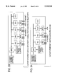
- FIG. 1 depicts an earlier implementation of a multi-port memory system in which k ports, each having word width m, equally share a common memory. Each burst includes k words. K memory access buffers each can store k m-bit words. Each buffer is connected to the shared memory by a k ⁇ m line wide path. The shared memory is k ⁇ m bits wide.
- FIG. 2 show a data format used in a typical multiport memory system such as that in FIG. 1.
- a k word burst of m-bit words passes through a port.
- the entire burst is briefly stored in a single memory access buffer.
- all k-words of the burst are simultaneously transferred from the buffer and written to the shared memory on the k ⁇ m path.
- k words are read from the shared memory during another prescribed time slot and are transferred to a single memory access buffer. Then the buffered data is transferred through the port associated with that buffer.
- the port which originally inputted the burst may be different from the port that outputs the burst.
- the shared memory temporarily stores the burst so that it can be routed from the input port to the output port.
- the system of FIG. 1 can be used to pass data between ports.
- k m-bit words received through a respective port are buffered by a memory access buffer assigned to that port. Subsequently, during a time slot reserved for that memory access buffer, all of the k m-bit words stored in the assigned buffer are simultaneously written to the shared memory on the shared k ⁇ m-bit wide path.
- each of the other buffers can store k m-bit words on behalf of their own associated ports. The entire contents (all k words) of each individual buffer can be written to the shared memory during the individual time slot reserved for that buffer.
- a memory read operation is analogous, with the steps of the write operation reversed.
- FIG. 3 is a block diagram depicting another conventional multi-port shared memory system.
- the data format used involves 16 word bursts of 72 bits per word (64-bit data plus 8-bit parity).
- the shared memory bus has a width of 1152 lines (16 words ⁇ 72 bits/word).
- the bus is connected to each of 16 memory access buffers.
- Each buffer would need more than 1224 data pins, 1152 to connect to the bus and 72 to connect to the port.
- the 1152 data pins connected to the bus would each require high drive capability to operate on a bus connected to all 16 buffers and to the shared memory.
- FIG. 3 shows an illustrative bus capacitance that must be overcome by the buffer pins.
- the architecture should require fewer pins for memory access buffers and should not require high drive capability for buffer pins.
- the present invention meets those needs.
- a novel memory interface unit includes a bus interface unit and a buffer which can store multiple data burst subsets in transit to or from a digital memory.
- a switch includes an externally accessible master data path which transfers data to or from the bus interface unit.
- An externally accessible slave data port transfers data to or from the buffer.
- a direct path transfers data between the bus interface unit and the buffer.
- FIG. 1 is a block diagram of an earlier multi-port shared memory system
- FIG. 2 is a data format which can be used in the earlier system of FIG. 1;
- FIG. 3 is a block diagram of another earlier multi-port shared memory system
- FIG. 4 is a generalized block diagram of a first multi-port shared memory system in accordance with the present invention.
- FIG. 5 shows a data format and data flow used in the embodiment of FIG. 4;
- FIG. 6 is a more detailed block diagram of memory access buffers and control logic of the embodiment of FIG. 4;
- FIG. 7 is a block diagram of a representative dual register pair of the memory access buffers of FIG. 6;
- FIG. 8 is a timing diagram which explains the operation of the control logic and memory access buffers of FIG. 6;
- FIG. 9 is a timing diagram which explains the operation of the dual register pairs of FIG. 7;
- FIG. 10 is a block diagram of an Asynchronous Transfer Mode switch in accordance with the present invention.
- FIG. 11 is a block diagram of a switch system which includes a memory interface unit (MIU) and associated control circuitry and registers in accordance with a presently preferred embodiment of the invention;
- MIU memory interface unit
- FIG. 12 is a simplified block diagram illustrating data lines and control lines of the embodiment of FIG. 11;
- FIG. 13 is a simplified block diagram showing one possible configuration of the configurable switch of the switch system of FIG. 11;
- FIG. 14A is a block diagram showing signal lines and control lines of the configurable switch of the embodiment of FIG. 11;
- FIG. 14B is a gate level logic diagram showing the logic gates within the configurable switch of FIG. 14A used to produce c0 during a memory write for a two MIU implementation;
- FIG. 14C is a gate level logic diagram showing the logic gates within the configurable switch of FIG. 14A used to produce d0 during a memory read for a two MIU implementation;
- FIG. 15 is an illustrative block diagram showing details of a transfer buffer of the embodiment of FIG. 11;
- FIG. 16 is an illustrative block diagram showing details of an individual memory access buffer of the transfer buffer of FIG. 15;
- FIG. 17 is a block diagram of a two MIU system in accordance with a present embodiment of the invention.
- FIG. 18 is a side view of stacked boxes containing the two MIU system of FIG. 17 which illustrates port and address connections between the two MIUs;
- FIG. 19 is a matrix that represents interconnections among configurable switches of the two MIU system of FIG. 17;
- FIG. 20 is a simplified block diagram of the two MIU system of FIG. 17 illustrating the flow of burst subsets during a memory write operation
- FIG. 21 is a timing diagram which illustrates the timing of data and control signals during a memory write operation for the two MIU system of FIG. 17;
- FIG. 22 is a simplified block diagram of the two MIU system of FIG. 17 illustrating the flow of subsets during a memory read operation
- FIG. 23 is a timing diagram which illustrates the timing of data and control signals in connection with a read operation for the two MIU system of FIG. 17;
- FIG. 24 is a simplified block diagram of a four MIU system in accordance with a present embodiment of the invention.
- FIG. 25 is a side view of stacked boxes containing the four MIU system of FIG. 24 which illustrates port and address connections between the MIUs;
- FIG. 26 is a matrix that represents interconnections among MIUs of the four MIU system of FIG. 24;
- FIG. 27 is a simplified block diagram illustrating the flow of burst subsets within the four MIU system of FIG. 24 during a read operation
- FIG. 28 is a timing diagram which illustrates the timing of data and control signals in connection with a read operation for the four MIU system of FIG. 24;
- FIG. 29 is a simplified block diagram illustrating the flow of burst subsets within the four MIU system of FIG. 24 during a memory write operation.
- FIG. 30 is a timing diagram which illustrates the timing of data and control signals in connection with a write operation for the four MIU system of FIG. 24;
- FIG. 31 illustrates a stand alone MIU application using the embodiment of FIG. 11;
- FIG. 32 illustrates a four MIU application using the embodiment of FIG. 11;
- FIG. 33 illustrates an Ethernet switch application using the embodiment of FIG. 11
- FIG. 34 illustrates an Ethernet switch with ATM uplink application using the embodiment of FIG. 11;
- FIG. 35 illustrates a two MIU stackable switch/router using the embodiment of FIG. 11;
- FIG. 36 illustrates a four MIU fast Ethernet switch using the embodiment of FIG. 11;
- FIG. 37 is an improved embodiment of the switch of FIG. 4, which employs time division multiplex (TDM) switching;
- TDM time division multiplex
- FIG. 38 is a timing diagram illustrating the operation of the switch of FIG. 37.
- FIG. 39 is an illustrative drawing of an embodiment of the switch of FIG. 4 in which individual byte subsets may be transmitted through a switch matrix multiple bits at a time.
- the present invention comprises a novel method and apparatus for implementing a multi-port shared memory system.
- the following description is presented to enable any person skilled in the art to make and use the invention. Descriptions of specific applications are provided only as examples. Various modifications to the preferred embodiment will be readily apparent to those skilled in the art, and the generic principles defined herein may be applied to other embodiments and applications without departing from the spirit and scope of the invention. Thus, the present invention is not intended to be limited to the embodiment shown, but is to be accorded the widest scope consistent with the principles and features disclosed herein.
- the first system 18 includes a set of k ports 20 each inputting/outputting m-bit data words in n-word bursts, an interconnection matrix circuit 22, a set of m memory access buffers 24, and a shared memory 26.
- a port serves as a two-way digital path on which digital information can be transferred to or from external circuitry such as a data bus. Port structures are well known to those skilled in the art and need not be described herein. Specific regions within the shared memory 26, indicated by dashed lines, are reserved for subsets of the data temporarily stored in the buffers 24.
- the ports 20 transfer binary data from individual external devices (not shown) connected thereto. These ports 20 provide the received binary data to the interconnection matrix 22, which distributes the data transferred through the ports among the memory access buffers 24. In the present embodiment, the distribution is accomplished such that each memory access buffer 24 receives a subset of the data transferred by each of the ports. In the present embodiment, each buffer 24 can transfer in parallel to memory 26 all of the data received by the buffer from an individual port. Moreover, all of the parallel transfers of data received from such an individual port can occur during a single memory access cycle.
- the memory read operation is analogous with the steps of the write operation, but reversed. That is, the bits for n m-bit words are transferred from the shared memory and are distributed among the memory access buffers 24.
- the interconnection matrix 22 then provides the distributed bits to a single port 20 through which a burst comprising n m-bit words is transferred to an external device (not shown).
- Each memory access buffer 24 is dedicated to storing a specific bit position for every data word transferred through any of the ports. Data words may contain data and parity information.
- the total number of memory access buffers 24 is equal to the total number of bits per word (m), thus allowing each buffer to be responsible for a single bit position in every word.
- memory access buffer 24-1 stores bit 1 (B1) of each word transferred through any of the ports 20-1 to 20-k; memory access buffer 24-2 stores bit 2 (B2) of each word transferred through any of ports 20-1 to 20-k; etc.
- each memory access buffer 24-1 through 24-m is connected to the shared memory 26 by a set of n data lines 28-1 through 28-k.
- the m-subsets, each subset with n bits, of different order bits can be simultaneously transferred between the memory 26 and the buffers 24.
- there are n-bits for each of the m-subsets that is, one bit for each of the n words in an n-word burst. Specifically, if there are n-words per burst, and there are m-bits per word then there are n-bits per burst of order B1, n-bits per burst of order B2, . . .
- n-bits per burst of order Bm All n-bits of a prescribed order can be simultaneously provided to the memory 26 on the n lines connected to a buffer assigned to store the bits of that order. For example, all n of the B1 bits are provided on the n lines connected to buffer 24-1. This means that the m buffers can transfer n words at a time to or from an addressed location of memory. As explained below, all of these transferred words would have originated at or been targeted to the same external device.
- Each port 20 transfers data in a prescribed format between the interconnect matrix 22 and external circuitry (not shown).
- a "port burst" shall mean a data burst transferred through a single port in either direction to or from the external circuitry.
- m-bit data words may be presented by a port to the interconnect matrix 22 for transfer to the buffers 24.
- m-bit data words may be presented to such a port by the interconnect matrix 22 for transfer to the external circuitry.
- the data word format involves, for each, data words bits B1 through Bm presented in a prescribed order.
- the interconnect matrix distributes the bits as described above.
- the interconnect matrix circuit 22 can be implemented using a printed circuit board (PCB), wire wrap or soldered wires.
- the interconnect matrix provides the connections between ports and buffers.
- each B1 in each word transferred through port 20-1 is connected by the matrix 22 to a storage element of buffer 24-1 associated with port 20-1;
- each B1 in each word transferred through port 20-2 is connected by the matrix 22 to a storage element of buffer 24-1 associated with port 20-2; . . .
- each B1 in each word transferred through port 20-k is connected by the matrix 22 to a storage element of buffer 24-1 associated with port 20-k.
- the memory access buffers can be implemented using either standard or custom logic.
- FIGS. 6-9 illustrate and explain the operation of the memory access buffers 24 and a representative dual register pair 34 of one of the memory access buffers 24.
- the illustrative block diagram of FIG. 6 shows the memory access buffers 24, control logic 29, serial input/output lines 30 connecting the buffers 24 to an interconnect matrix (not shown) and a n-bit parallel input/output bus 32.
- the control logic 29 controls serial I/O on lines 30 and parallel I/O on bus 32. The operation of the control logic will be explained with reference to the timing diagram of FIG. 8.
- each memory access buffer 24 includes k dual register pairs like the one shown in FIG. 7 for a total of 2 k registers per buffer 24.
- Each register pair in each buffer is associated with one of the ports.
- Each register pair is dedicated to storing all bits in a prescribed location (order) in every data word transferred to or from the port associated with that register pair. That is, each respective dual register pair of a respective buffer stores and transfers all of the same order bits from each data word transferred through a respective port.
- dual register pair R i1 receives and stores the first (in order) bit B1 of each data word transferred through port P i (not shown).
- dual register pair R i2 receives and stores the second (in order) bit B2 of each word transferred through port P i .
- dual register pair R im receives and stores the m th (in order) bit Bm of each word transferred through port P i .
- all B1s transferred through port P i represent a subset of the data transferred through that port.
- all B2s represent another subset as do all B m , for example.
- the dual register pair 34 includes a shift-in register 36 and a shift-out register 38.
- the shift-in register 36 first stores and then asserts in parallel n bits of data onto the memory bus 32 to be written into the shared memory 26.
- the shift-out register reads in parallel and stores n bits of data from the memory bus 32 which have been read "out" of the shared memory 26.
- the data stored in the shift-in register 36 is serially shifted from the interconnect matrix 22 into the shift-in register 36; and from there, it is asserted in parallel onto the bus 32 to be written into the memory 26 as described above.
- the data stored in the shift-out register 38 is read in parallel from the bus 32 into the shift-out register after it has been read from the memory 26; and from there, it is serially shifted from the shift-out register to the interconnect matrix 22.
- Output enable buffer 40 controls the serial transfer of data from the shift-out register 38 to the interconnect matrix 22.
- FIG. 8 there is shown a timing diagram for the memory access buffers 24-1 to 24-m of FIGS. 4-6.
- memory access alternates between 32 memory read cycles followed by 32 memory write cycles.
- each port has a clock cycle during which data transferred through that port can be written to memory 26. Consecutive ports' data are written on consecutive clock cycles, which are the respective write "time slots" for the respective ports.
- each port can begin transferring data to the memory access buffers thirty-two clock cycles before its time slot, so that there is sufficient time to transfer all thirty-two words of a burst received by a port to the m buffer registers (each located in a different memory access buffer) assigned to the port before the arrival of the port's time slot.
- B1 of W32 transferred through port 20-1 is serially written to the same register pair of buffer 24-1 as was B1 of W1 transferred through port 20-1.
- B6 of W3 transferred through port 20-1 is serially written to the same register pair in memory access buffer 24-6 (not shown) as was B6 of W1 transferred through port 20-1.
- r1.C is the read "time slot" for port 20-1.
- r31.C represents the read time slot for port 20-31.
- a shift-out register in buffer 24-1 receives in parallel all B1s of the thirty-two words read in parallel from the memory 26.
- a shift-out register in buffer 24-18 receives in parallel all B18s of the thirty-two words read in parallel from the memory 26.
- the interconnect matrix distributes the data word bits among buffers 24-l to 24-m so that each buffer only stores a subset of each word to be stored.
- each buffer stores only bits of a prescribed order.
- each buffer need only provide to the bus 32 a subset of all of the data to be simultaneously transferred to memory.
- the interconnect matrix recombines the bits distributed among multiple buffers so that they are outputted as a series (or burst) of complete words.
- the entire data to be transferred out through a port is outputted in parallel from the memory and is inputted to the buffers.
- each buffer only receives a subset of that entire data.
- the interconnect matrix 22 recombines the subsets into a burst of data words.
- each of the m respective buffers simultaneously connects one n-bit subset at a time to its parallel bus 32.
- the illustrative timning diagram of FIG. 9, shows the operation of the dual register pair of FIG. 7.
- P.WRITE pulse data that has been read from the shared memory 26 during an (rX.c) Memory Data Cycle is written in parallel into the shift-out register 38.
- each SHIFT-OUT pulse a single bit is shifted out from the shift-out register to the interconnect matrix 22 for transfer to a respective port.
- each SHIFT-OUT pulse corresponds to an r1.X pulse in FIG. 8.
- each SHIFT-IN pulse a single bit of data is shifted in to the shift-in register.
- each SHIFT-IN pulse corresponds to a w1.X pulse in FIG. 8.
- P.READ pulse all of the data that has been shifted in to the shift-in register can be read in parallel to be written to the shared memory 26 during a w1.C cycle.
- the shared memory 26 can be a standard random access memory (RAM) configuration with a memory width of (n ⁇ m).
- RAM random access memory
- the memory is able to transfer (n ⁇ m) bits of data to or from the memory access buffers 24 simultaneously, and is able to store all (n ⁇ m) bits in a single addressed location of memory, as depicted in FIG. 5.
- the words are "interleaved", so that all the first order bits (B1s) are stored contiguously, followed by all of the second order bits (B2s), and so forth.
- all of the bits representing the n words from or to a specific port 20 can be readily stored as a line of the shared memory 26.
- time slots are pre-assigned. However, time slots could be arbitrated based on priorities.
- each of the k ports 20 requires a single clock cycle time slot to communicate with the shared memory 26, and each port requires n clock cycles prior to that time slot to transfer an entire n-word data burst to or from the memory access buffers 24, it is efficient to set the number of words per burst (n) equal to the number of ports (k), thereby providing a smooth, cyclical process for transferring data without bottlenecks or idle times.
- the relationship between the number of ports and words per burst can change, however, without departing from the invention.
- FIGS. 10 is a block diagram of 32-port Asynchronous Transfer Mode (ATM) switch in accordance with the present invention.
- ATM is a payload multiplexing technique for information transfer using fixed-size packets, called cells.
- an ATM cell is 53-bytes long and consists of a 5byte header which carries the routing information, followed by a 48-byte information field (payload).
- the payload of each ATM cell entering the switch is placed in a specific location in the shared memory.
- This implementation was selected to have a 32-bit bus from the memory access buffers to the memory with each port word 12-bits wide, and with port bursts of thirty-two words. Note that 384 is also equal to (12 ⁇ 32); that is, a cell is transferred in a 32-word burst of 12-bit words.
- the ATM switch routes each received cell on a port to a destination port according to routing information that is included in each such cell. More particularly, a cell is transferred from a port and stored in shared memory. Then it is retrieved from the shared memory and is transferred to a destination port indicated in the cell. In this manner, data can be switched between ports.
- the operation of the control memory and the switch controller will be understood by those skilled in the art, form no part of the invention and need not be described herein.
- FIG. 11 shows a block diagram of a switch system 98 which includes a memory interface unit (MIU) 100 in accordance with a presently preferred embodiment of the invention.
- the MIU 100 includes a configurable switch 104 and a data transfer buffer 106.
- a bus interface register 102 is coupled to transfer digital information to and from a burst mode bus 108.
- the data transfer buffer 106 is coupled to temporarily store data in transit between a digital memory (not shown) and the configurable switch 104.
- Digital data is transferred to and from the memory via an i/o driver 110.
- An address register 112 receives digital address information from the bus 108. Address information received by the register 112 is provided to the digital memory via another i/o driver 114.
- a control unit 116 controls the operation of the MIU 100 and the memory.
- the configurable switch 104 of a present embodiment of the invention is selectively configurable to transfer burst subsets between the bus interface register 102 and either the transfer buffer 106 or the master (m n ) interconnects of ports p0, p1 or p2.
- the switch 104 is further configurable to transfer burst subsets between the transfer buffer 106 and either the bus interface register 102 or the slave interconnects (s n ) of ports p0, p1 or p2.
- the switch 104 can be placed in any of three different configurations: stand alone, 2 MIU and 4 MIU. In the stand alone configuration data is passed directly through the switch 104 from lines b0-b3 to lines c0-c3.
- the connections in the two MIU case are illustrated in FIG. 19.
- the connections in the four MIU cases are illustrated in FIG. 26.
- the switch system of the present invention permits the sharing of memory among different ports, where each port is connected to a different burst mode bus.
- a burst mode bus such as PCI, SBUS or GIO, for example, permits the provision of an address which accompanies the data provided on the bus.
- individual MIUs can be "chained” together or “stacked” in order to coordinate access to a shared memory by devices connected to different burst mode buses.
- FIG. 12 is an illustrative block diagram showing in more detail the data lines and control lines of the switch system 98 of FIG. 11.
- the system 98 transfers signals to and from a bus.
- the bus is a PCI bus.
- the MIU can communicate with other types of burst mode buses such as SBUS, GIO, etc.
- Data, address and Read/Write control signals can be provided to a digital memory connected to the switch system 98.
- the system 98 includes three ports, p0, p1 and p2 that can, for example, be used to transfer signals to other switch systems (not shown).
- Each port includes eight master data lines and one master request line.
- Each port also includes eight slave data lines and one slave request line.
- Data is transferred to and from the transfer buffer 106 shown in FIG. 11. Addresses are provided by the address register 112. R/W signals are generated by the controller 116.
- the port interconnects provide access to the configurable switch 104.
- the operation of the novel switch system 98 shall be explained by first detailing a memory write operation and then detailing a memory read operation.
- a burst of digital information is transferred from the bus 108 to the bus interface register 102.
- the bus 108 is 32-bits wide, and the burst may include a 32-bit wide address word followed by four 32-bit wide data words.
- the burst is transferred, via the multibit lines labeled b0, b1, b2 and b3, to the configurable switch 104.
- the switch 104 can be configured to transfer certain subsets of the burst via one or more of the multibit lines labeled c0, c1, c2 and c3, directly to the data transfer buffer 106.
- the switch 104 also can be configured to provide the remaining subsets of the burst to one or more other switch systems (not shown) associated with other memories (not shown) via one or more of the master interconnects labeled m0, m1, and m2, respectively accessible through port 0, port 1 and port 2.
- the subsets provided to other switch systems via the master interconnect(s) are stored in the digital memories associated with those other systems. The storage of subsets transferred to other memories shall be discussed below in connection with exemplary two MIU and four MIU systems.
- the transfer buffer 106 temporarily stores the subsets transferred to it, and then provides them, via one or more of the multibit lines labeled d0, d1, d2 and d3, to the i/o driver 110 which presents them for storage in a digital memory associated with switch system 98.
- Digital address signals received from the bus 108 in conjunction with the burst are used to designate the memory locations where the subsets are to be stored.
- the same memory address is used for both the memory associated with switch system 98 and for other memories associated with other switch systems.
- different subsets of the burst may be stored at the same address in different memories.
- the subsets of a burst may he distributed among several distinct digital memories (not shown in FIG. 11) that are accessible through several different switch systems (not shown in FIG. 11).
- an address signal is placed on the bus. The address is received through address register 112 and is provided to each of these distinct memories.
- FIG. 11 shows only a single switch system 98 that provides access to a single one of these memories. As explained below, there may be other similar switch systems connected to provide access to other memories.
- the address signal is used to retrieve distinct burst subsets from the distinct memories in which they are stored.
- Burst subsets stored in the memory accessed through switch system 98 are presented by that memory to the i/o driver 110 which transfers such subsets, via one or more of the multibit lines d0, d1, d2 and d3, to the transfer buffer 106 for temporary storage.
- the buffer 106 presents those subsets to the configurable switch 104 via one or more of the multibit lines c0, c1, c2 and c3.
- the configurable switch 104 can be configured to provide them directly to one or more of the multibit lines b0, b1, b2 and b3 connected to the bus interface register 102.
- the subsets that are not stored in the memory accessed through the switch system 98 are transferred to the switch system 98 via one or more of the multibit slave interconnects labeled s0, s1 and s2 of port1, port2 or port3, respectively. More particularly, those subsets stored in other memories are first retrieved from those memories and then are transferred to one or more of the slave interconnects of the switch system 98. The retrieval of subsets from these other memories shall be discussed below in connection with exemplary two MIU and four MIU systems.
- the configurable switch 104 can be configured to transfer subsets provided on its slave interconnects to one or more of the multibit lines b0, b1, b2 and b3, to the register 102.
- FIG. 13 is a simplified block diagram of the bus interface register 102, the configurable switch 104 and the transfer buffer 106 of FIG. 11 showing one possible configuration of a switch 104 in accordance with a current embodiment of the invention.
- the switch 104 (indicated within dashed lines) is configured to transfer burst subsets between the buffer 106 and register 102 via a "direct" interconnect path 105.
- Master interconnects m0, m1 and m2 provide paths for the transfer of burst subsets to and from the register 102.
- Slave interconnects s0, s1 and s2 provide paths for the transfer of burst subsets to and from the transfer buffer 106.
- a burst is received by the bus interface register 102.
- a first burst subset is transferred via the direct path 105 to the buffer 106.
- a second burst subset is transferred away from the register 102 via master path m0.
- a third burst subset is transferred away from the register via master path m1.
- a fourth burst subset is transferred away from the register via master path m2.
- the first burst subset can be stored in a memory (not shown) connected to the buffer 106, and the second, third and fourth burst subsets can be stored elsewhere, in memories accessed via paths m0, m1 and m2.
- a first burst subset initially is stored in a memory (not shown) connected to the buffer 106, and second, third and fourth burst subsets are stored elsewhere in different digital memories (not shown).
- the transfer buffer 106 can temporarily store the first subset when it is retrieved from the memory connected to that buffer 106.
- the buffer then transfers the first subset to the register via the direct path 105.
- a second burst subset is received via slave path s0.
- a third burst subset is received via slave path s1.
- a fourth subset is received via slave path s2.
- FIG. 13 represents only one possible configuration of the switch 104.
- the switch might instead be configured to provide multiple direct paths between the bus interface logic 116 and the buffer 106.
- the discussion below in connection with a two MIU system 120 and a four MIU system 106 explains a few exemplary alternative switch configurations.
- FIG. 14A there is shown a block diagram of a configurable switch 104 of a currently preferred embodiment which illustrates many of the signal lines of the switch 104.
- the switch is implemented as a multiplexer in a manner that will be readily appreciated by one of ordinary skill in the art.
- FIG. 14B is a gate level logic diagram that illustrates the internal logic responsible for producing the c0 output during a "read” operation by a two MIU implementation described below.
- FIG. 14C is a gate level logic diagram that illustrates the internal logic responsible for producing the b0 output during a "write” operation by a two MIU implementation described below.
- the P0 input for example, may designate the right side MIU, and P1 may designate the left side MIU.
- the buffer 106 includes four memory access buffers 106-1, 106-2, 106-3 and 106-4.
- the memory access buffers receive respective P -- READ, P -- WRITE, OE(0-3) and W(0-3) control signals.
- the configurable switch 104 accesses memory access buffers which are accessible via byte-wide input/output lines c0, c1, c2 and c3. In a current implementation each serial line is one byte wide. However, different sized multibit fragments of a burst subset are possible.
- the memory (not shown) is accessed through the memory access buffers via lines d0, d1, d2 and d3, over an 32-bit memory bus 224.
- the memory bus 224 transfers digital information between individual memory access buffers and a digital memory (not shown) connected to the buffer 106.
- a burst subset might be transferred in parallel (all at once) from memory access buffer 106-1 to the memory via bus 224.
- the burst subset might be transferred in parallel (all at once) from the memory to memory access buffer 106-1 via the bus 224.
- a shift-in register 226 receives a series of byte-wide burst subset fragments on lines c1 until an entire burst subset is accumulated.
- the shift-in register can temporarily store the complete burst subset.
- the entire subset then is asserted in parallel (all byte-wide fragments at once) to the memory bus 224 so that the subset can be written in parallel to the digital memory.
- a shift-out register 228 is employed during memory reads. An entire burst subset read from the memory is provided in parallel to the shift-out register 228 the memory bus 224.
- the shift-out register can temporarily store the entire burst subset. The register then can provide a series of byte-wide burst subset fragments on lines c1 until the entire burst subset has been delivered to the configurable switch 104.
- Output buffer 230 controls the provision of subset fragments from the shift-out register to lines c1.
- each individual switch system includes a control unit that issues control signals that control the operation of its associated transfer buffer. If there are multiple switch systems connected together as, for example in the two MIU configuration or the four MIU configuration, then coordination among the controllers of the different switch systems is required in order to achieve sharing of memory. This coordination can be achieved, for instance, by having each controller run an algorithm used to coordinate the multiple switch systems access to shared memory. There are several well known algorithms that can be employed. For example, requests for memory access by different switch systems can be handled according to a fixed priority among switches or according to a round-robin scheme.
- FIG. 17 is an illustrative block diagram of a two MIU system 120 in accordance with a present embodiment of the invention. For simplicity sake, details such as the control logic and the bus interface logic are not shown.
- Two MIUs 122 and 124 are interconnected as shown. That is, the MIU switches 123 and 125 are configured so that m0 and s0 interconnects of MIU switch 123 and MIU switch 125 are connected to each other through their respective ports p0. Similarly, the m2 and s2 interconnects of MIU switch 123 and MIU switch 125 are connected to each other through their respective ports p2.
- Switch 123 is further configured to provide direct interconnects 141 and 142 between bus interface logic 126 and buffer 130.
- Switch 125 is further configured to provide direct interconnects 143 and 144 between bus interface logic 128 and buffer 132.
- Buffer 130 is connected to transfer burst subsets to and from digital memory 134.
- Buffer 132 is connected to transfer burst subsets to and from digital memory 136.
- FIG. 18 is a simplified side view of two stacked boxes 156 and 158 which together house the two MIU system 120.
- Box 156 houses MIU 122, memory 134 and bus interface logic 126.
- Box 158 houses MIU 124, memory 136 and bus interface logic 128.
- Each box 156 and 158 has three ports p0, p1, and p3.
- Each box also has a shared address bus over which it can share address information with a neighboring box or boxes. The ports p0 and the ports p2 and the shared address bus are connected as shown.
- FIG. 19 is a matrix that represents the interconnections among the two MIUs 122 and 124 of the two MIU system of FIG. 17.
- a "0" at a line intersection indicates an interconnection within MIU switch 123.
- a "1" at a line intersection indicates an interconnection within MIU switch 125.
- the upper left quadrant represents connections between slave lines s0, s1, and s2 and bus interface logic lines b0, b1, b2 and b3.
- the lower right quadrant represents connections between master lines m0, m1 and m2 and MIU buffer lines c0, c1, c2 and c3.
- the lower left quadrant represents connections between bus interface logic lines b0, b1, b2 and b3 and MIU buffer lines c0, c1, c2 and c3.
- the interconnections for MIU switch 123 are as follows: b0 directly connected to c0; b1 connected to m0; b2 directly connected to c2; b3 connected to m2; c1 connected to s0; and c3 connected to s2.
- the interconnections for MIU switch 125 are as follows: b0 connected to m0; b1 connected directly to c1; b2 connected to m2; b3 connected directly to c3; c0 connected to s0; and c2 connected to s2.
- bursts are transferred between the MIUs 122 and 124 and an external bus (not shown) via bus interface logic units 126 and 128.
- bus interface logic units 126 and 128 For simplicity sake, the address and data registers connected to an external bus are shown to be amalgamated into bus interface logic units.
- An entire exemplary four word burst 127 transferred through logic 126 is shown.
- the burst 127 includes the digital word identified as containing multibit fragments A00, A01 A02 and A03.
- each fragment includes multiple logical bits.
- the invention may be implemented using single bit fragments as an alternative.
- the burst subset which includes A00, A10, A20 and A30 and the burst subset which includes A02, A12, A12 and A32 are transferred between the bus interface logic 126 and the buffer 130 via direct interconnects 141 and 142.
- the burst subset which includes A01, A11, A21 and A31 is transferred between the bus interface logic 126 and the buffer 132 via the port p0 interconnects of the switches 123 and 125.
- the burst subset which includes A03, A13, A23 and A33 is transferred between the bus interface logic 126 and the buffer 132 via the port p2 interconnects of the switches 123 and 125.
- the burst includes the digital word identified as containing multibit fragments B00, B01, B02 and B03.
- the burst subset which includes B00, B10, B20 and B30 and the burst subset which includes B02, B12, B12 and B32 are transferred between the bus interface logic 128 and the buffer 132 via direct interconnects 143 and 145.
- the burst subset which includes B01, B11, B21 and B31 is transferred between the bus interface logic 128 and the buffer 130 via the port p0 interconnects of the switches 123 and 125.
- the burst subset which includes B03, B13, B23 and B33 is transferred between the bus interface logic 128 and the buffer 130 via the port p2 interconnects of the switches 123 and 125.
- Two subsets from the burst 127 transferred though bus interface logic 126 and two subsets from the burst 129 transferred through bus interface logic 128 can be temporarily stored in each of the two buffers 130 and 132 as shown.
- the two subsets from each of the bursts are stored in digital memory 134, and two subsets from each of the two bursts are stored in digital memory 136 as shown.
- SRAM is employed.
- other memory architectures such as DRAM could be used consistent with the invention.
- FIG. 20 illustrates the flow of burst subsets through the two MIU system 120 of FIG. 17 during a representative memory write operation.
- a five word burst 146 is received by the bus interface logic (not shown).
- the first word of the burst contains address information.
- the next four words contain digital information to be written to digital memories 134 and 136.
- the address information is transferred by MIU 122 to an MIU address register 148.
- the MIU address register 148 presents the burst address to memory address registers 150 and 152 of digital memories 134 and 136 via connection 154.
- Burst subset d00, d10, d20 and d30 and burst subset d02, d2, d22 and d32 are transferred by MIU 122 to digital memory 134 for storage at an address location designated by memory address register 150.
- Burst subset d31, d21, d11 and d01 is transferred from MIU 122 to MIU 124 via their respective port p0 interconnects, and then is transferred by MIU 124 to digital memory 136 for storage at a memory location designated by memory address register 152.
- burst subset d33, d23, d13 and d03 is transferred from MUW 122 to MIU 124 via their respective port p2 interconnects, and then is transferred by MIU 124 to digital memory 136 for storage at a memory location designated by memory address register 152.
- Each of the burst subsets transferred from MIU 122 to MIU 124 is preceded by a Rq signal, which indicates whether there is to be a read or a write.
- FIG. 21 is a timing diagram which illustrates the timing of data and control signals in connection with the memory write operation of FIG. 17 for the two M system 120 of FIG. 17.
- an address is received from the bus.
- data word D0 is received from the segment bus; and the Rq signals are sent over the p0 and p2 interconnects to MIU 124.
- data word D1 is received from the segment bus, and burst subset fragments d01 and d03 are transferred to MIU 124 over the multibit master interconnects of ports p0 and p2 respectively.
- data word D2 is received from the segment bus, and burst subset fragments d11 and d13 are transferred to MIU 124 over the multibit master interconnects of ports p0 and p2 respectively.
- data word D3 is received from the segment bus, and burst subset fragments d21 and d23 are transferred to MIU 124 over the multibit master interconnects of ports p0 and p2 respectively.
- burst subset fragments d31 and d33 are transferred to MIU 124 over the multibit master interconnects of ports p0 and p2 respectively.
- a memory address associated with the burst in registers 150 and 154 is presented to each of the digital memories 134 and 136.
- a memory write enable signal is asserted simultaneously by two control units that control the two MIUs, and the entire data burst subsets stored in the transfer buffers 130 and 132 are written in parallel to the respective digital memories 134 and 136.
- FIG. 22 illustrates the flow of burst subsets through the two MIU system 120 of FIG. 17 during a representative memory read operation.
- the four words of a burst are distributed across two different digital memories 134 and 136.
- a memory address 125 is provided to MIU address buffer 148 which presents the address via the connection 154 to memory address registers 150 and 152.
- Digital memory 134 provides the burst subset d00, d10, d20 and d30 to MIU 122 which transfers it directly to the bus interface logic 126.
- Digital memory 134 also provides the burst subset d02, d12, d22 and d32 to MIU 122 which transfers it directly to the bus interface logic (not shown).
- Digital memory 136 transfers burst subset d01, d11, d21 and d31 to MIU 124 which transfers it to MIU 122 via their port p0 interconnects. MIU 122 then transfers the subset to its bus interface logic. Similarly, digital memory 136 transfers burst subset d03, d13, d23 and d33 to MIU 124 which transfers it to MIU 122 via their port p2 interconnects. MIU 122 then transfers the subset to its bus interface logic. Thus, the burst 146 is retrieved from different memories and is made available at the bus interface logic.
- FIG. 23 is a timing diagram which illustrates the timing of data and control signals in connection with the memory read operation of FIG. 22 for the two MIU system 120 of FIG. 17.
- an address signal is received from the segment bus.
- Rq signals produced by the bus interface logic are sent over the p0 and p2 interconnects of MIU 124.
- a memory address in each of memory address registers 150 and 152 is presented to memories 134 and 136.
- a memory output enable signal is provided to each of the memories, and entire data burst subsets are read in parallel from each of the two memories 134 and 136 and are presented to transfer buffers 130 and 132 for temporary storage.
- fragments d01 and d03 are transferred to MIU 122 over the slave interconnects of ports p0 and p2 respectively.
- fragments d11 and d13 are transferred to MIU 122 over the slave interconnects of ports p0 and p2 respectively, and data word DO is presented to the segment bus.
- fragments d21 and d23 are transferred to MIU 122 over the slave interconnects of ports p0 and p2 respectively, and data word D1 is presented to the segment bus.
- FIG. 24 is a simplified block diagram of a four MIU system 160 in accordance with a presently preferred embodiment of the invention. Control logic and bus interface logic details are omitted to simplify the following explanation.
- the system 160 includes four MIUs 162, 164, 166 and 168. Each MIU includes a configurable matrix of electrical interconnect lines. Every MIU includes three ports, p0, p1 and p2. Each MIU also includes a buffer section 186, 188, 190 and 192. Each of the four MIUs is connected to a different one of four digital memories 170, 172, 174 and 176. Each of the four MIUs also is connected to a different one of four bus interface logic units 178, 180, 182 and 184.
- FIG. 25 is a side view of four stacked boxes 194, 196, 198 and 200 which together house the four MIU system 160 of FIG. 23.
- Box 194 houses MIU 162, memory 170 and bus interface logic 178.
- Box 196 houses MIU 164, memory 172 and bus interface logic 180.
- Box 198 houses MIU 166, memory 174 and bus interface logic 182.
- Box 200 houses MIU 168, memory 176 and bus interface logic 184.
- Each box has three ports p0, p1, and p2.
- Each box also has an address bus over which it can share address information with a neighboring box. The ports and the address buses are connected as shown.
- the port p1 interconnects of MIU 162 in box 194 and MIU 166 in box 198 are coupled to transfer burst subsets between the two MIUs.
- the port p1 master interconnect of MIU 162 is coupled to the port p1 slave interconnect of MIU 166.
- the port p1 slave interconnect of MIU 162 is coupled to the port p1 master interconnect of MIU 166.
- the burst segment A02, A12, A22, A32 is transmitted between bus interface logic 178 and digital memory 174 via the port p1 master interconnect of MIU 162 and the port p1 slave interconnect of MIU 166.
- the burst segment C00, C10, C20, C30 is transmitted between bus interface logic 182 and digital memory 170 via the port p1 slave interconnect of MIU 162 and the port p1 master interconnect of MIU 166.
- FIG. 26 is a matrix that represents the interconnections among the four MIUs 162, 164, 166 and 168 of the four MIU system 160 of FIG. 24.
- a "0" at a line intersection indicates an interconnection within MIU switch 162.
- a “1” at a line intersection indicates an interconnection within MIU switch 164.
- a “2” at a line intersection indicates an interconnection within MIU switch 166.
- a “3" at a line intersection indicates an interconnection within MIU 168.
- the interconnections for MIU switch 162 are as follows: b0 connected directly to c0; c1 connected to s0; c2 connected to s1; c3 connected to s2; b1 connected to m0; b2 connected to m1; and b3 connected to m2.
- the interconnections for MIU switch 166 are as follows: b0 connected to m2; b1 connected to m1; b2 connected to m0; b3 connected directly to c3; c0 connected to s2; c1 connected to s1; and c2 connected to s0.
- the interconnections of MIUs 164 and 168 will be readily appreciated from the matrix of FIG. 22 and the above discussion.
- the operation of the four MIU system 160 of FIG. 24 in transferring burst subsets can be appreciated by observing the bursts transferred through bus interface logic 178, 180, 182 and 184; by observing the distribution of burst subsets among buffers 186, 188, 190 and 192; and by observing the storage of burst subsets in digital memories 170, 172, 174 and 176.
- subset A01, A11, A21, A31 is transferred through bus interface logic 178 as part of a four word burst.
- Subset B01, B11, B21, B31 is transferred through bus interface logic 180 as part of a four word burst.
- Subset C01, C11, C21, C31 is transferred through bus interface logic 182 as part of a four word burst.
- Subset D01, D11, D21, D31 is transferred through bus interface logic 184 as part of a four word burst.
- the subset is temporarily stored in buffer 188.
- FIG. 27 illustrates the flow of burst subsets through the four MIU system 160 of FIG. 24 during a representative memory write operation.
- a five word burst is received by bus interface logic associated with MIU 162.
- the first word of the burst contains address information.
- the next four words are slated to be distributed among digital memories 170, 172, 174 and 176.
- the address information is transferred by MIU 162 to an MIU address register 204.
- the MIU address register 204 presents the address to memory address registers 206, 208 210 and 212 of digital memories 172, 174, 176 and 178 via bus 214.
- Burst subset d00, d10, d20 and d30 is transferred by MIU 162 directly to digital memory 170 for storage at an address location designated by memory address register 206.
- Burst subset d31, d21, d11 and d01 is transferred from MIU 162 to MIU 164 via their respective port p0 interconnects, and then is transferred by MIU 164 to digital memory 172 for storage at a memory location designated by memory address register 208.
- Burst subset d02, d2, d22 and d32 is transferred from MIU 162 to MIU 166 via their respective port p1 interconnects, and then is transferred by MIU 166 to digital memory 174 for storage at a memory location designated by memory address register 210.
- Burst subset d33, d23, d13 and d03 is transferred from MIU 162 to MIU 168 via their respective port p2 interconnects, and then is transferred by MIU 168 to digital memory 176 for storage at a memory location designated by memory address register 212.
- Each of the burst subsets transferred among MIUs is preceded by a Rq signal which indicates whether there is to be a memory read or a memory write.
- FIG. 28 is a timing diagram which illustrates the timing of data and control signals in connection with the memory write operation of FIG. 27 for the four MIU system 160 of FIG. 24.
- an address is received from the segment bus.
- data word DO is received from the segment bus, and the Rq signals are sent over the p0, p1 and p2 interconnects to MIUs 164, 166 and 168.
- data word D1 is received from the segment bus, and burst subset fragments d01, d02 and d03 are transferred to MIUs 164, 166 and 168 over the multibit master interconnects of ports p0, p1 and p2 respectively.
- data word D2 is received from the segment bus, and burst subset fragments d11, d12 and d13 are transferred to MIUs 164, 166 and 168 over the multibit master interconnects of arts p0, p1 and p2 respectively.
- data word D3 is received from the segment bus, and burst subset fragments d21, d22 and d23 are transferred to MIUs 164, 166 and 168 over the multibit master interconnects of ports p0, p1 and p2 respectively.
- burst subset fragments d31, d32 and d33 are transferred to MIUs 164, 166 and 168 over the multibit master interconnects of ports p0, p1 and p2 respectively.
- a memory address in registers 206, 208, 210 and 212 is presented to each of the digital memories 170, 172, 174 and 176.
- a memory write enable signal is asserted simultaneously by the control units associated with each of the MIUs and entire data burst subsets stored in the transfer buffers 186, 188, 190 and 192 are written in parallel to the respective digital memories 170, 172, 174 and 176.
- FIG. 29 illustrates the flow of burst subsets through the four MIU system 160 of FIG. 24 during a representative memory read operation.
- the four words of a burst are distributed across four different digital memories 170, 172, 174 and 176.
- a memory address 216 is provided to MIU address buffer 204 which presents the address via the connection 214 to memory address registers 206, 208, 210 and 212.
- Digital memory 170 provides the burst subset d00, d10, d20 and d30 to MIU 162 and then transfers it directly to its bus interface logic (not shown).
- Digital memory 172 provides the burst subset d01, d11, d21 and d31 to MIU 164 which transfers it to MIU 162 via port p0 interconnects. MIU 162 then transfers the subset to its bus interface logic. Digital memory 174 transfers burst subset d02, d2, d22 and d32 to MIU 166 which transfers it to MIU 162 via port p1 interconnects. MIU 162 then transfers the subset to its bus interface logic. Digital memory 176 transfers burst subset d03, d13, d23 and d33 to MIU 168 which then transfers it to MIU 162 via port p2 interconnects. MIU 162 then transfers the subset to its bus interface logic. Thus, the burst 202 is retrieved from different memories and is made available at the bus interface logic of MIU 162.
- FIG. 30 is a timing diagram which illustrates the timing of data and control signals in connection with the memory read operation of FIG. 29 for the four MIU system 160 of FIG. 24.
- an address signal is received from the segment bus.
- Rq signals produced by the bus interface logic are sent over the p0, p1 and p2 interconnects of MIU 162.
- a memory address in each of memory address registers 206, 208, 210 and 212 is presented to memories 170, 172, 174 and 176.
- a memory output enable signal is provided to each of the memories, and entire data burst subsets are read in parallel from each of the four memories 170, 172, 174 and 176 and are presented to transfer buffers 186, 188, 190 and 192 for temporary storage.
- fragments d01, d02 and d03 are transferred to MIU 162 over the slave interconnects of ports p0, p1 and p2 respectively.
- fragments d11, d12 and d13 are transferred to MIU 162 over the slave interconnects of ports p0, p1 and p2 respectively, and data word DO is presented to the segment bus.
- fragments d21, d22 and d23 are transferred to MIU 162 over the slave interconnects of ports p0, p1 and p2 respectively, and data word Dl is presented to the segment bus.
- fragments d31, d32 and d33 are transferred to MIU 162 over the slave interconnects of ports p0, p1 and p2 respectively, and data word D2 is presented to the segment bus.
- data word D3 is presented to the segment bus.
- FIGS. 31-36 illustrate some possible applications of the present invention. In these Figures switch system 98 is referred to as a Queue Management Unit ("QMU") in implementing shared memory.
- QMU Queue Management Unit
- FIG. 31 shows the use of a basic switch in a stand alone configuration.
- FIG. 32 illustrates a four MIU (four QMU) stacked configuration.
- FIG. 33 illustrates an Ethernet switch implementation.
- FIG. 34 illustrates an Ethernet switch with ATM uplink.
- FIG. 35 illustrates a two MIU (two QMU) stackable switcwrouter.
- FIG. 36 illustrates a four MIU (four QMU) fast Ethernet switch with address resolution (ARL).
- ARL address resolution
- FIG. 37 An improved apparatus is illustrated in FIG. 37 which combines two shared memory switches to result in a non-blocking larger switch with twice the bandwidth (e.g., combine two 32 ⁇ 32 155-Mbps port ATM switches to construct a non-blocking 64 ⁇ 64 155-Mbps port ATM switch, for example).
- a present embodiment involves a 32 ⁇ 32 ATM switch.
- the 32 ⁇ 32 ATM switch operates in a time division multiplex (TDM) fashion.
- TDM time division multiplex
- the switch cycles in 68-clock periods, divided into 32-clock input stage and 32-clock output stage (and a 4-clock gap). Take two 32 ⁇ 32 switch chipsets and two banks of shared memory. Make each 32 ⁇ 32 chipset be able to access any of the two banks.
- matrix interconnect lines between a port and a buffer may be multiple bits wide for each burst segment. Hence multiple bits per burst segment may be transferred per clock cycle.
Landscapes
- Engineering & Computer Science (AREA)
- Theoretical Computer Science (AREA)
- Computer Networks & Wireless Communication (AREA)
- Signal Processing (AREA)
- Physics & Mathematics (AREA)
- General Physics & Mathematics (AREA)
- General Engineering & Computer Science (AREA)
- Mathematical Physics (AREA)
- Data Exchanges In Wide-Area Networks (AREA)
- Information Transfer Systems (AREA)
- Multi Processors (AREA)
- Static Random-Access Memory (AREA)
- Memory System (AREA)
- Bus Control (AREA)
Abstract
Description
c0=P1·s0+P0·b0
c1=P0·s0+P1·b1
c2=P1·s2+P0·b2
c3=P0·s2+P1·b3
m0=P1·b0+P0·b1
m2=P1·b2+P0·b3
b0=P1·m0+P0·c0
b1=P0·m0+P1·c1
b2=P1·m2+P0·c2
b3=P0·m2+P1·c3
s0=P1·c0+P0·c1
s2=P1·c2+P0·c3
Claims (21)
Priority Applications (2)
| Application Number | Priority Date | Filing Date | Title |
|---|---|---|---|
| US08/998,586 US5910928A (en) | 1993-08-19 | 1997-12-29 | Memory interface unit, shared memory switch system and associated method |
| US09/133,287 US6021086A (en) | 1993-08-19 | 1998-08-12 | Memory interface unit, shared memory switch system and associated method |
Applications Claiming Priority (3)
| Application Number | Priority Date | Filing Date | Title |
|---|---|---|---|
| US08/109,805 US5440523A (en) | 1993-08-19 | 1993-08-19 | Multiple-port shared memory interface and associated method |
| US08/512,613 US5732041A (en) | 1993-08-19 | 1995-08-07 | Memory interface unit, shared memory switch system and associated method |
| US08/998,586 US5910928A (en) | 1993-08-19 | 1997-12-29 | Memory interface unit, shared memory switch system and associated method |
Related Parent Applications (1)
| Application Number | Title | Priority Date | Filing Date |
|---|---|---|---|
| US08/512,613 Continuation US5732041A (en) | 1993-08-19 | 1995-08-07 | Memory interface unit, shared memory switch system and associated method |
Related Child Applications (1)
| Application Number | Title | Priority Date | Filing Date |
|---|---|---|---|
| US09/133,287 Continuation US6021086A (en) | 1993-08-19 | 1998-08-12 | Memory interface unit, shared memory switch system and associated method |
Publications (1)
| Publication Number | Publication Date |
|---|---|
| US5910928A true US5910928A (en) | 1999-06-08 |
Family
ID=24039837
Family Applications (3)
| Application Number | Title | Priority Date | Filing Date |
|---|---|---|---|
| US08/512,613 Expired - Lifetime US5732041A (en) | 1993-08-19 | 1995-08-07 | Memory interface unit, shared memory switch system and associated method |
| US08/998,586 Expired - Lifetime US5910928A (en) | 1993-08-19 | 1997-12-29 | Memory interface unit, shared memory switch system and associated method |
| US09/133,287 Expired - Lifetime US6021086A (en) | 1993-08-19 | 1998-08-12 | Memory interface unit, shared memory switch system and associated method |
Family Applications Before (1)
| Application Number | Title | Priority Date | Filing Date |
|---|---|---|---|
| US08/512,613 Expired - Lifetime US5732041A (en) | 1993-08-19 | 1995-08-07 | Memory interface unit, shared memory switch system and associated method |
Family Applications After (1)
| Application Number | Title | Priority Date | Filing Date |
|---|---|---|---|
| US09/133,287 Expired - Lifetime US6021086A (en) | 1993-08-19 | 1998-08-12 | Memory interface unit, shared memory switch system and associated method |
Country Status (7)
| Country | Link |
|---|---|
| US (3) | US5732041A (en) |
| EP (2) | EP0843854B1 (en) |
| JP (2) | JP3628706B2 (en) |
| KR (1) | KR100356447B1 (en) |
| AU (1) | AU6590596A (en) |
| DE (2) | DE69631055T2 (en) |
| WO (1) | WO1997006489A1 (en) |
Cited By (17)
| Publication number | Priority date | Publication date | Assignee | Title |
|---|---|---|---|---|
| US6021086A (en) * | 1993-08-19 | 2000-02-01 | Mmc Networks, Inc. | Memory interface unit, shared memory switch system and associated method |
| DE19936080A1 (en) * | 1999-07-30 | 2001-02-15 | Siemens Ag | Multiprocessor system for performing memory accesses to a shared memory and associated method |
| WO2001069849A2 (en) * | 2000-03-15 | 2001-09-20 | Broadcom Corporation | Method and apparatus for shared buffer packet switching |
| WO2001091390A2 (en) * | 2000-05-19 | 2001-11-29 | Engedi Networks, Inc. | Pipelined and sliced shared-memory switch |
| EP1179929A2 (en) * | 2000-08-11 | 2002-02-13 | Marconi Communications, Inc. | Transferring and queueing length and data as one stream |
| US6473838B1 (en) | 2000-01-04 | 2002-10-29 | International Business Machines Corporation | Data transfer system for multiple network processors using dual DRAM storage |
| US20020163833A1 (en) * | 2000-03-21 | 2002-11-07 | Stmicroelectronics S.R.L. | String programmable nonvolatile memory with NOR architecture |
| US6535516B1 (en) * | 1998-12-10 | 2003-03-18 | Industrial Technology Research Institute | Shared memory based network switch and the network constructed with the same |
| US6571302B1 (en) | 2000-04-04 | 2003-05-27 | Advanced Digital Information Corporation | Dynamic adjustment of multiple sequential burst data transfers |
| US20030167408A1 (en) * | 2002-03-01 | 2003-09-04 | Fitzpatrick Gregory P. | Randomized bit dispersal of sensitive data sets |
| US6711646B1 (en) * | 2000-10-20 | 2004-03-23 | Sun Microsystems, Inc. | Dual mode (registered/unbuffered) memory interface |
| US20050102469A1 (en) * | 2003-11-12 | 2005-05-12 | Ofir Zohar | Distributed task queues in a multiple-port storage system |
| US7031330B1 (en) * | 1999-04-15 | 2006-04-18 | Marconi Intellectual Property (Ringfence), Inc. | Very wide memory TDM switching system |
| US20080247411A1 (en) * | 2007-03-31 | 2008-10-09 | International Business Machines Corporation | Method to operate a crossbar switch |
| US7761754B1 (en) * | 2008-03-25 | 2010-07-20 | Altera Corporation | Techniques for testing memory circuits |
| US20140143512A1 (en) * | 2012-11-16 | 2014-05-22 | International Business Machines Corporation | Accessing additional memory space with multiple processors |
| US8990516B2 (en) | 2010-03-25 | 2015-03-24 | Fujitsu Limited | Multi-core shared memory system with memory port to memory space mapping |
Families Citing this family (65)
| Publication number | Priority date | Publication date | Assignee | Title |
|---|---|---|---|---|
| US5719890A (en) * | 1995-06-01 | 1998-02-17 | Micron Technology, Inc. | Method and circuit for transferring data with dynamic parity generation and checking scheme in multi-port DRAM |
| TW301090B (en) * | 1996-08-14 | 1997-03-21 | Winbond Electronics Corp | Data storing and searching method of ethernet switch mean address table and device thereof |
| US6230245B1 (en) | 1997-02-11 | 2001-05-08 | Micron Technology, Inc. | Method and apparatus for generating a variable sequence of memory device command signals |
| US6487207B1 (en) * | 1997-02-26 | 2002-11-26 | Micron Technology, Inc. | Shared buffer memory architecture for asynchronous transfer mode switching and multiplexing technology |
| US6175894B1 (en) | 1997-03-05 | 2001-01-16 | Micron Technology, Inc. | Memory device command buffer apparatus and method and memory devices and computer systems using same |
| US5825711A (en) * | 1997-06-13 | 1998-10-20 | Micron Technology, Inc. | Method and system for storing and processing multiple memory addresses |
| US5996043A (en) * | 1997-06-13 | 1999-11-30 | Micron Technology, Inc. | Two step memory device command buffer apparatus and method and memory devices and computer systems using same |
| US6484244B1 (en) | 1997-06-17 | 2002-11-19 | Micron Technology, Inc. | Method and system for storing and processing multiple memory commands |
| US6170046B1 (en) | 1997-10-28 | 2001-01-02 | Mmc Networks, Inc. | Accessing a memory system via a data or address bus that provides access to more than one part |
| US6202119B1 (en) | 1997-12-19 | 2001-03-13 | Micron Technology, Inc. | Method and system for processing pipelined memory commands |
| US6088285A (en) * | 1998-01-20 | 2000-07-11 | Oki Electric Industry Co., Ltd. | Semiconductor memory circuit in which pattern widths of switching circuit and buffers are formed within a pattern width of a column unit |
| US6138219A (en) * | 1998-03-27 | 2000-10-24 | Nexabit Networks Llc | Method of and operating architectural enhancement for multi-port internally cached dynamic random access memory (AMPIC DRAM) systems, eliminating external control paths and random memory addressing, while providing zero bus contention for DRAM access |
| US6173425B1 (en) | 1998-04-15 | 2001-01-09 | Integrated Device Technology, Inc. | Methods of testing integrated circuits to include data traversal path identification information and related status information in test data streams |
| US6216205B1 (en) | 1998-05-21 | 2001-04-10 | Integrated Device Technology, Inc. | Methods of controlling memory buffers having tri-port cache arrays therein |
| US5982700A (en) * | 1998-05-21 | 1999-11-09 | Integrated Device Technology, Inc. | Buffer memory arrays having nonlinear columns for providing parallel data access capability and methods of operating same |
| US5978307A (en) * | 1998-05-21 | 1999-11-02 | Integrated Device Technology, Inc. | Integrated circuit memory devices having partitioned multi-port memory arrays therein for increasing data bandwidth and methods of operating same |
| US5999478A (en) * | 1998-05-21 | 1999-12-07 | Integrated Device Technology, Inc. | Highly integrated tri-port memory buffers having fast fall-through capability and methods of operating same |
| US6434145B1 (en) | 1998-06-22 | 2002-08-13 | Applied Micro Circuits Corporation | Processing of network data by parallel processing channels |
| US6175905B1 (en) | 1998-07-30 | 2001-01-16 | Micron Technology, Inc. | Method and system for bypassing pipelines in a pipelined memory command generator |
| US6178488B1 (en) | 1998-08-27 | 2001-01-23 | Micron Technology, Inc. | Method and apparatus for processing pipelined memory commands |
| WO2000017726A2 (en) * | 1998-09-18 | 2000-03-30 | Computron | Switchable master/slave memory controller |
| US6233236B1 (en) * | 1999-01-12 | 2001-05-15 | Mcdata Corporation | Method and apparatus for measuring traffic within a switch |
| US7382736B2 (en) * | 1999-01-12 | 2008-06-03 | Mcdata Corporation | Method for scoring queued frames for selective transmission through a switch |
| US6757791B1 (en) * | 1999-03-30 | 2004-06-29 | Cisco Technology, Inc. | Method and apparatus for reordering packet data units in storage queues for reading and writing memory |
| FR2797969A1 (en) * | 1999-08-31 | 2001-03-02 | Koninkl Philips Electronics Nv | DEVICE WITH MULTIPLE PROCESSORS SHARING A COLLECTIVE MEMORY |
| JP3881477B2 (en) | 1999-09-06 | 2007-02-14 | 沖電気工業株式会社 | Serial access memory |
| US6771654B1 (en) * | 2000-01-24 | 2004-08-03 | Advanced Micro Devices, Inc. | Apparatus and method for sharing memory using a single ring data bus connection configuration |
| US6735207B1 (en) * | 2000-06-13 | 2004-05-11 | Cisco Technology, Inc. | Apparatus and method for reducing queuing memory access cycles using a distributed queue structure |
| US7006505B1 (en) * | 2000-10-23 | 2006-02-28 | Bay Microsystems, Inc. | Memory management system and algorithm for network processor architecture |
| US6546461B1 (en) | 2000-11-22 | 2003-04-08 | Integrated Device Technology, Inc. | Multi-port cache memory devices and FIFO memory devices having multi-port cache memory devices therein |
| US6515914B2 (en) * | 2001-03-21 | 2003-02-04 | Micron Technology, Inc. | Memory device and method having data path with multiple prefetch I/O configurations |
| US7139267B2 (en) * | 2002-03-05 | 2006-11-21 | Industrial Technology Research Institute | System and method of stacking network switches |
| US7283556B2 (en) * | 2001-07-31 | 2007-10-16 | Nishan Systems, Inc. | Method and system for managing time division multiplexing (TDM) timeslots in a network switch |
| US7215666B1 (en) * | 2001-11-13 | 2007-05-08 | Nortel Networks Limited | Data burst scheduling |
| JP2005517242A (en) * | 2002-02-06 | 2005-06-09 | コーニンクレッカ フィリップス エレクトロニクス エヌ ヴィ | Address space, bus system, memory controller and device system |
| US7110415B1 (en) | 2002-05-17 | 2006-09-19 | Marvell International Ltd. | Apparatus and method for dynamically limiting output queue size in a quality of service network |
| DE60216772T2 (en) * | 2002-10-22 | 2007-08-30 | Hewlett-Packard Development Co., L.P., Houston | Method and apparatus for operating a telecommunications platform |
| US7571287B2 (en) * | 2003-03-13 | 2009-08-04 | Marvell World Trade Ltd. | Multiport memory architecture, devices and systems including the same, and methods of using the same |
| EP1513072A3 (en) * | 2003-09-02 | 2009-10-21 | Thomson Licensing | Method for multibank memory scheduling |
| US7707330B2 (en) * | 2003-09-18 | 2010-04-27 | Rao G R Mohan | Memories for electronic systems |
| US7042792B2 (en) * | 2004-01-14 | 2006-05-09 | Integrated Device Technology, Inc. | Multi-port memory cells for use in FIFO applications that support data transfers between cache and supplemental memory arrays |
| DE102004038211A1 (en) * | 2004-08-05 | 2006-03-16 | Robert Bosch Gmbh | Message manager and method for controlling the access to data of a message memory of a communication module |
| US20070239906A1 (en) * | 2006-03-13 | 2007-10-11 | Vakil Kersi H | Input/output agent having multiple secondary ports |
| US7769942B2 (en) | 2006-07-27 | 2010-08-03 | Rambus, Inc. | Cross-threaded memory system |
| US8234425B1 (en) | 2007-06-27 | 2012-07-31 | Marvell International Ltd. | Arbiter module |
| US7949817B1 (en) | 2007-07-31 | 2011-05-24 | Marvell International Ltd. | Adaptive bus profiler |
| US8219778B2 (en) * | 2008-02-27 | 2012-07-10 | Microchip Technology Incorporated | Virtual memory interface |
| US8131915B1 (en) | 2008-04-11 | 2012-03-06 | Marvell Intentional Ltd. | Modifying or overwriting data stored in flash memory |
| US8683085B1 (en) | 2008-05-06 | 2014-03-25 | Marvell International Ltd. | USB interface configurable for host or device mode |
| JP5332430B2 (en) * | 2008-09-11 | 2013-11-06 | 富士通株式会社 | Shared memory system |
| TWI393142B (en) * | 2008-12-29 | 2013-04-11 | Macronix Int Co Ltd | Memory device and control method of memory device |
| WO2010093538A1 (en) | 2009-02-11 | 2010-08-19 | Rambus Inc. | Shared access memory scheme |
| US8423710B1 (en) | 2009-03-23 | 2013-04-16 | Marvell International Ltd. | Sequential writes to flash memory |
| US8213236B1 (en) | 2009-04-21 | 2012-07-03 | Marvell International Ltd. | Flash memory |
| US8688922B1 (en) | 2010-03-11 | 2014-04-01 | Marvell International Ltd | Hardware-supported memory management |
| US8756394B1 (en) | 2010-07-07 | 2014-06-17 | Marvell International Ltd. | Multi-dimension memory timing tuner |
| JP5229922B2 (en) * | 2010-11-08 | 2013-07-03 | ルネサスエレクトロニクス株式会社 | Information processing system |
| US8645609B2 (en) * | 2010-12-06 | 2014-02-04 | Brocade Communications Systems, Inc. | Two-port memory implemented with single-port memory blocks |
| JP5948345B2 (en) | 2011-01-11 | 2016-07-06 | エイ10 ネットワークス インコーポレイテッドA10 Networks, Inc. | Virtual application delivery chassis system |
| US9154577B2 (en) | 2011-06-06 | 2015-10-06 | A10 Networks, Inc. | Sychronization of configuration file of virtual application distribution chassis |
| US9961130B2 (en) | 2014-04-24 | 2018-05-01 | A10 Networks, Inc. | Distributed high availability processing methods for service sessions |
| US10742559B2 (en) | 2014-04-24 | 2020-08-11 | A10 Networks, Inc. | Eliminating data traffic redirection in scalable clusters |
| CN105740177B (en) * | 2014-12-08 | 2019-05-21 | 台湾积体电路制造股份有限公司 | The control method and device and signal latch device of signal transmission |
| KR20160071290A (en) | 2014-12-11 | 2016-06-21 | (주)두린 | Roller thermal insulation structure of sliding window |
| US10318288B2 (en) | 2016-01-13 | 2019-06-11 | A10 Networks, Inc. | System and method to process a chain of network applications |
Citations (16)
| Publication number | Priority date | Publication date | Assignee | Title |
|---|---|---|---|---|
| EP0187518A2 (en) * | 1984-12-24 | 1986-07-16 | Sony Corporation | Data processor system and method |
| US4744078A (en) * | 1985-05-13 | 1988-05-10 | Gould Inc. | Multiple path multiplexed host to network data communication system |
| US4750154A (en) * | 1984-07-10 | 1988-06-07 | Prime Computer, Inc. | Memory alignment system and method |
| US4754451A (en) * | 1986-08-06 | 1988-06-28 | American Telephone And Telegraph Company, At&T Bell Laboratories | N-by-N "knockout" switch for a high-performance packet switching system with variable length packets |
| US4760570A (en) * | 1986-08-06 | 1988-07-26 | American Telephone & Telegraph Company, At&T Bell Laboratories | N-by-N "knockout" switch for a high-performance packet switching system |
| US4888741A (en) * | 1988-12-27 | 1989-12-19 | Harris Corporation | Memory with cache register interface structure |
| US4891794A (en) * | 1988-06-20 | 1990-01-02 | Micron Technology, Inc. | Three port random access memory |
| US4891795A (en) * | 1987-05-21 | 1990-01-02 | Texas Instruments Incorporated | Dual-port memory having pipelined serial output |
| US5142638A (en) * | 1989-02-07 | 1992-08-25 | Cray Research, Inc. | Apparatus for sharing memory in a multiprocessor system |
| US5204841A (en) * | 1990-07-27 | 1993-04-20 | International Business Machines Corporation | Virtual multi-port RAM |
| JPH05151769A (en) * | 1991-11-28 | 1993-06-18 | Mitsubishi Electric Corp | Multi port memory |
| US5278967A (en) * | 1990-08-31 | 1994-01-11 | International Business Machines Corporation | System for providing gapless data transfer from page-mode dynamic random access memories |
| US5337287A (en) * | 1991-08-20 | 1994-08-09 | Nec Corporation | Dual port semiconductor memory device |
| WO1995005635A1 (en) * | 1993-08-19 | 1995-02-23 | Mmc Networks, Inc. | Multiple-port shared memory interface and associated method |
| US5634004A (en) * | 1994-05-16 | 1997-05-27 | Network Programs, Inc. | Directly programmable distribution element |
| US5732041A (en) * | 1993-08-19 | 1998-03-24 | Mmc Networks, Inc. | Memory interface unit, shared memory switch system and associated method |
Family Cites Families (6)
| Publication number | Priority date | Publication date | Assignee | Title |
|---|---|---|---|---|
| GB2200483B (en) * | 1987-01-22 | 1991-10-16 | Nat Semiconductor Corp | Memory referencing in a high performance microprocessor |
| US4958341A (en) * | 1988-03-31 | 1990-09-18 | At&T Bell Laboratories | Integrated packetized voice and data switching system |
| IT1259342B (en) * | 1992-03-17 | 1996-03-12 | Cselt & Centro Studi E Lab Tel | HIGH SPEED CELL SWITCHING ELEMENT IN CMOS TECHNOLOGY |
| US5742760A (en) * | 1992-05-12 | 1998-04-21 | Compaq Computer Corporation | Network packet switch using shared memory for repeating and bridging packets at media rate |
| US5309395A (en) * | 1992-10-22 | 1994-05-03 | At&T Bell Laboratories | Synchronous static random access memory |
| US5802052A (en) * | 1996-06-26 | 1998-09-01 | Level One Communication, Inc. | Scalable high performance switch element for a shared memory packet or ATM cell switch fabric |
-
1995
- 1995-08-07 US US08/512,613 patent/US5732041A/en not_active Expired - Lifetime
-
1996
- 1996-07-18 KR KR10-1998-0700888A patent/KR100356447B1/en not_active IP Right Cessation
- 1996-07-18 JP JP50844797A patent/JP3628706B2/en not_active Expired - Lifetime
- 1996-07-18 DE DE69631055T patent/DE69631055T2/en not_active Expired - Lifetime
- 1996-07-18 WO PCT/US1996/011974 patent/WO1997006489A1/en active IP Right Grant
- 1996-07-18 EP EP96925380A patent/EP0843854B1/en not_active Expired - Lifetime
- 1996-07-18 DE DE1028380T patent/DE1028380T1/en active Pending
- 1996-07-18 AU AU65905/96A patent/AU6590596A/en not_active Abandoned
- 1996-07-18 EP EP00200593A patent/EP1028380A3/en not_active Withdrawn
-
1997
- 1997-12-29 US US08/998,586 patent/US5910928A/en not_active Expired - Lifetime
-
1998
- 1998-08-12 US US09/133,287 patent/US6021086A/en not_active Expired - Lifetime
-
2004
- 2004-04-27 JP JP2004131369A patent/JP3899085B2/en not_active Expired - Lifetime
Patent Citations (17)
| Publication number | Priority date | Publication date | Assignee | Title |
|---|---|---|---|---|
| US4750154A (en) * | 1984-07-10 | 1988-06-07 | Prime Computer, Inc. | Memory alignment system and method |
| EP0187518A2 (en) * | 1984-12-24 | 1986-07-16 | Sony Corporation | Data processor system and method |
| US4744078A (en) * | 1985-05-13 | 1988-05-10 | Gould Inc. | Multiple path multiplexed host to network data communication system |
| US4754451A (en) * | 1986-08-06 | 1988-06-28 | American Telephone And Telegraph Company, At&T Bell Laboratories | N-by-N "knockout" switch for a high-performance packet switching system with variable length packets |
| US4760570A (en) * | 1986-08-06 | 1988-07-26 | American Telephone & Telegraph Company, At&T Bell Laboratories | N-by-N "knockout" switch for a high-performance packet switching system |
| US4891795A (en) * | 1987-05-21 | 1990-01-02 | Texas Instruments Incorporated | Dual-port memory having pipelined serial output |
| US4891794A (en) * | 1988-06-20 | 1990-01-02 | Micron Technology, Inc. | Three port random access memory |
| US4888741A (en) * | 1988-12-27 | 1989-12-19 | Harris Corporation | Memory with cache register interface structure |
| US5142638A (en) * | 1989-02-07 | 1992-08-25 | Cray Research, Inc. | Apparatus for sharing memory in a multiprocessor system |
| US5204841A (en) * | 1990-07-27 | 1993-04-20 | International Business Machines Corporation | Virtual multi-port RAM |
| US5278967A (en) * | 1990-08-31 | 1994-01-11 | International Business Machines Corporation | System for providing gapless data transfer from page-mode dynamic random access memories |
| US5337287A (en) * | 1991-08-20 | 1994-08-09 | Nec Corporation | Dual port semiconductor memory device |
| JPH05151769A (en) * | 1991-11-28 | 1993-06-18 | Mitsubishi Electric Corp | Multi port memory |
| WO1995005635A1 (en) * | 1993-08-19 | 1995-02-23 | Mmc Networks, Inc. | Multiple-port shared memory interface and associated method |
| US5440523A (en) * | 1993-08-19 | 1995-08-08 | Multimedia Communications, Inc. | Multiple-port shared memory interface and associated method |
| US5732041A (en) * | 1993-08-19 | 1998-03-24 | Mmc Networks, Inc. | Memory interface unit, shared memory switch system and associated method |
| US5634004A (en) * | 1994-05-16 | 1997-05-27 | Network Programs, Inc. | Directly programmable distribution element |
Non-Patent Citations (3)
| Title |
|---|
| International Search Report PCT/US94/09364 (which cites Schiffleger and EP A0187518 above ). * |
| Translation of Japanese patent document No. 5 151769 (Kubo). * |
| Translation of Japanese patent document No. 5-151769 (Kubo). |
Cited By (34)
| Publication number | Priority date | Publication date | Assignee | Title |
|---|---|---|---|---|
| US6021086A (en) * | 1993-08-19 | 2000-02-01 | Mmc Networks, Inc. | Memory interface unit, shared memory switch system and associated method |
| US6535516B1 (en) * | 1998-12-10 | 2003-03-18 | Industrial Technology Research Institute | Shared memory based network switch and the network constructed with the same |
| US7031330B1 (en) * | 1999-04-15 | 2006-04-18 | Marconi Intellectual Property (Ringfence), Inc. | Very wide memory TDM switching system |
| DE19936080A1 (en) * | 1999-07-30 | 2001-02-15 | Siemens Ag | Multiprocessor system for performing memory accesses to a shared memory and associated method |
| US6473838B1 (en) | 2000-01-04 | 2002-10-29 | International Business Machines Corporation | Data transfer system for multiple network processors using dual DRAM storage |
| WO2001069849A2 (en) * | 2000-03-15 | 2001-09-20 | Broadcom Corporation | Method and apparatus for shared buffer packet switching |
| US7315550B2 (en) | 2000-03-15 | 2008-01-01 | Broadcom Corporation | Method and apparatus for shared buffer packet switching |
| WO2001069849A3 (en) * | 2000-03-15 | 2002-01-10 | Broadcom Corp | Method and apparatus for shared buffer packet switching |
| US6700894B1 (en) | 2000-03-15 | 2004-03-02 | Broadcom Corporation | Method and apparatus for shared buffer packet switching |
| US20040130949A1 (en) * | 2000-03-21 | 2004-07-08 | Stmicroelectronics S.R.L. | String programmable nonvolatile memory with NOR architecture |
| US20020163833A1 (en) * | 2000-03-21 | 2002-11-07 | Stmicroelectronics S.R.L. | String programmable nonvolatile memory with NOR architecture |
| US7072212B2 (en) | 2000-03-21 | 2006-07-04 | Stmicroelectronics S.R.L. | String programmable nonvolatile memory with NOR architecture |
| US6683808B2 (en) * | 2000-03-21 | 2004-01-27 | Stmicroelectronics S.R.L. | String programmable nonvolatile memory with NOR architecture |
| US6954395B2 (en) | 2000-03-21 | 2005-10-11 | Stmicroelectronics S.R.L. | String programmable nonvolatile memory with NOR architecture |
| US20040130948A1 (en) * | 2000-03-21 | 2004-07-08 | Stmicroelectronics S.R.I. | String programmable nonvolatile memory with NOR architecture |
| US6571302B1 (en) | 2000-04-04 | 2003-05-27 | Advanced Digital Information Corporation | Dynamic adjustment of multiple sequential burst data transfers |
| WO2001091390A3 (en) * | 2000-05-19 | 2002-04-18 | Engedi Networks Inc | Pipelined and sliced shared-memory switch |
| WO2001091390A2 (en) * | 2000-05-19 | 2001-11-29 | Engedi Networks, Inc. | Pipelined and sliced shared-memory switch |
| EP1179929A3 (en) * | 2000-08-11 | 2002-05-15 | Marconi Communications, Inc. | Transferring and queueing length and data as one stream |
| EP1179929A2 (en) * | 2000-08-11 | 2002-02-13 | Marconi Communications, Inc. | Transferring and queueing length and data as one stream |
| US7035267B1 (en) | 2000-08-11 | 2006-04-25 | Marconi Intellectual Property (Ringfence), Inc. | Transferring and queueing length and data as one stream |
| US6711646B1 (en) * | 2000-10-20 | 2004-03-23 | Sun Microsystems, Inc. | Dual mode (registered/unbuffered) memory interface |
| US20030167408A1 (en) * | 2002-03-01 | 2003-09-04 | Fitzpatrick Gregory P. | Randomized bit dispersal of sensitive data sets |
| US20050102469A1 (en) * | 2003-11-12 | 2005-05-12 | Ofir Zohar | Distributed task queues in a multiple-port storage system |
| US7870334B2 (en) * | 2003-11-12 | 2011-01-11 | International Business Machines Corporation | Distributed task queues in a multiple-port storage system |
| US7978690B2 (en) * | 2007-03-31 | 2011-07-12 | International Business Machines Corporation | Method to operate a crossbar switch |
| US20080247411A1 (en) * | 2007-03-31 | 2008-10-09 | International Business Machines Corporation | Method to operate a crossbar switch |
| US7761754B1 (en) * | 2008-03-25 | 2010-07-20 | Altera Corporation | Techniques for testing memory circuits |
| US7984344B1 (en) * | 2008-03-25 | 2011-07-19 | Altera Corporation | Techniques for testing memory circuits |
| US8990516B2 (en) | 2010-03-25 | 2015-03-24 | Fujitsu Limited | Multi-core shared memory system with memory port to memory space mapping |
| US20140143512A1 (en) * | 2012-11-16 | 2014-05-22 | International Business Machines Corporation | Accessing additional memory space with multiple processors |
| US20140143510A1 (en) * | 2012-11-16 | 2014-05-22 | International Business Machines Corporation | Accessing additional memory space with multiple processors |
| US9047057B2 (en) * | 2012-11-16 | 2015-06-02 | International Business Machines Corporation | Accessing additional memory space with multiple processors |
| US9052840B2 (en) * | 2012-11-16 | 2015-06-09 | International Business Machines Corporation | Accessing additional memory space with multiple processors |
Also Published As
| Publication number | Publication date |
|---|---|
| WO1997006489A1 (en) | 1997-02-20 |
| EP0843854B1 (en) | 2003-12-10 |
| DE69631055D1 (en) | 2004-01-22 |
| KR19990036220A (en) | 1999-05-25 |
| EP1028380A3 (en) | 2005-11-09 |
| EP0843854A1 (en) | 1998-05-27 |
| JP3628706B2 (en) | 2005-03-16 |
| EP1028380A2 (en) | 2000-08-16 |
| DE1028380T1 (en) | 2001-04-19 |
| KR100356447B1 (en) | 2003-04-10 |
| JPH11510285A (en) | 1999-09-07 |
| JP3899085B2 (en) | 2007-03-28 |
| AU6590596A (en) | 1997-03-05 |
| DE69631055T2 (en) | 2004-07-08 |
| US6021086A (en) | 2000-02-01 |
| US5732041A (en) | 1998-03-24 |
| JP2004320786A (en) | 2004-11-11 |
Similar Documents
| Publication | Publication Date | Title |
|---|---|---|
| US5910928A (en) | Memory interface unit, shared memory switch system and associated method | |
| US5440523A (en) | Multiple-port shared memory interface and associated method | |
| JP4024875B2 (en) | Method and apparatus for arbitrating access to shared memory for network ports operating at different data rates | |
| US6408367B2 (en) | Data path architecture and arbitration scheme for providing access to a shared system resource | |
| EP0195589B1 (en) | Switching system for transmission of data | |
| US6438613B1 (en) | Method and apparatus for allowing packet data to be separated over multiple bus targets | |
| EP1001347A2 (en) | Data processing device with memory coupling unit | |
| JPH03139044A (en) | Switch circuit net for atm system and switch circuit net module | |
| JPH0638607B2 (en) | Packet switched multi-port memory NxM switch node and processing method | |
| EP0460853B1 (en) | Memory system | |
| JP2002049582A (en) | Reconstructible first-in/first-out mechanism | |
| US6920510B2 (en) | Time sharing a single port memory among a plurality of ports | |
| JPH0581121A (en) | First-in first-out type memory-buffer | |
| US7535898B2 (en) | Distributed switch memory architecture | |
| US5721841A (en) | Adapter having data aligner including register being loaded to or from memory with an offset in accordance with predetermined network fragmentation parameters | |
| GB2397668A (en) | Processor array with delay elements | |
| US6680939B1 (en) | Expandable router | |
| JPH05274279A (en) | Device for parallel processing and device therefor | |
| JP3133234B2 (en) | ATM switch address generation circuit | |
| JPH0865318A (en) | Non-synchronous transfer mode data cell routing device | |
| US6465989B1 (en) | Apparatus for integrating switch ports in an ATM switching system | |
| TW594779B (en) | Multi-bank semiconductor memory device having plural buses and method of reducing bus loading | |
| JPS6366661A (en) | Storage control system | |
| JPH07143135A (en) | Atm switch device | |
| JPH0573406A (en) | Non-alignment data transfer device |
Legal Events
| Date | Code | Title | Description |
|---|---|---|---|
| STCF | Information on status: patent grant |
Free format text: PATENTED CASE |
|
| FEPP | Fee payment procedure |
Free format text: PAT HOLDER NO LONGER CLAIMS SMALL ENTITY STATUS, ENTITY STATUS SET TO UNDISCOUNTED (ORIGINAL EVENT CODE: STOL); ENTITY STATUS OF PATENT OWNER: LARGE ENTITY |
|
| FPAY | Fee payment |
Year of fee payment: 4 |
|
| SULP | Surcharge for late payment | ||
| REMI | Maintenance fee reminder mailed | ||
| FPAY | Fee payment |
Year of fee payment: 8 |
|
| AS | Assignment |
Owner name: QUALCOMM INCORPORATED, CALIFORNIA Free format text: ASSIGNMENT OF ASSIGNORS INTEREST;ASSIGNOR:APPLIED MICRO CIRCUITS CORPORATION;REEL/FRAME:021876/0013 Effective date: 20080715 Owner name: QUALCOMM INCORPORATED,CALIFORNIA Free format text: ASSIGNMENT OF ASSIGNORS INTEREST;ASSIGNOR:APPLIED MICRO CIRCUITS CORPORATION;REEL/FRAME:021876/0013 Effective date: 20080715 |
|
| AS | Assignment |
Owner name: MMC NETWORKS, INC., CALIFORNIA Free format text: ASSIGNMENT OF ASSIGNORS INTEREST;ASSIGNOR:JOFFE, ALEXANDER;REEL/FRAME:022703/0218 Effective date: 19951130 Owner name: AMCC SWITCHING & NETWORK PROCESSING CORPORATION, C Free format text: CHANGE OF NAME;ASSIGNOR:MMC NETWORKS, INC.;REEL/FRAME:022703/0328 Effective date: 20010815 |
|
| AS | Assignment |
Owner name: APPLIED MICRO CIRCUITS CORPORATION, CALIFORNIA Free format text: MERGER;ASSIGNOR:AMCC SWITCHING & NETWORK PROCESSING CORPORATION;REEL/FRAME:022783/0364 Effective date: 20020311 |
|
| FPAY | Fee payment |
Year of fee payment: 12 |