EP0997947A1 - Cellule DRAM à condensateur ensillonné - Google Patents
Cellule DRAM à condensateur ensillonné Download PDFInfo
- Publication number
- EP0997947A1 EP0997947A1 EP99308160A EP99308160A EP0997947A1 EP 0997947 A1 EP0997947 A1 EP 0997947A1 EP 99308160 A EP99308160 A EP 99308160A EP 99308160 A EP99308160 A EP 99308160A EP 0997947 A1 EP0997947 A1 EP 0997947A1
- Authority
- EP
- European Patent Office
- Prior art keywords
- trench
- memory device
- semiconductor memory
- recited
- region
- Prior art date
- Legal status (The legal status is an assumption and is not a legal conclusion. Google has not performed a legal analysis and makes no representation as to the accuracy of the status listed.)
- Granted
Links
Images


Classifications
-
- H—ELECTRICITY
- H10—SEMICONDUCTOR DEVICES; ELECTRIC SOLID-STATE DEVICES NOT OTHERWISE PROVIDED FOR
- H10B—ELECTRONIC MEMORY DEVICES
- H10B12/00—Dynamic random access memory [DRAM] devices
-
- H—ELECTRICITY
- H10—SEMICONDUCTOR DEVICES; ELECTRIC SOLID-STATE DEVICES NOT OTHERWISE PROVIDED FOR
- H10B—ELECTRONIC MEMORY DEVICES
- H10B12/00—Dynamic random access memory [DRAM] devices
- H10B12/30—DRAM devices comprising one-transistor - one-capacitor [1T-1C] memory cells
- H10B12/37—DRAM devices comprising one-transistor - one-capacitor [1T-1C] memory cells the capacitor being at least partially in a trench in the substrate
- H10B12/373—DRAM devices comprising one-transistor - one-capacitor [1T-1C] memory cells the capacitor being at least partially in a trench in the substrate the capacitor extending under or around the transistor
-
- H—ELECTRICITY
- H10—SEMICONDUCTOR DEVICES; ELECTRIC SOLID-STATE DEVICES NOT OTHERWISE PROVIDED FOR
- H10B—ELECTRONIC MEMORY DEVICES
- H10B12/00—Dynamic random access memory [DRAM] devices
- H10B12/01—Manufacture or treatment
- H10B12/02—Manufacture or treatment for one transistor one-capacitor [1T-1C] memory cells
- H10B12/03—Making the capacitor or connections thereto
- H10B12/038—Making the capacitor or connections thereto the capacitor being in a trench in the substrate
Definitions
- This invention is related to semiconductor memory devices, and more particularly, to a memory cell structure which uses the field-effect controlled majority carrier depletion of a buried strap region to control the access to a trench-cell capacitor.
- DRAMs typically include a switching transistor coupled to a storage capacitor structure.
- trench storage have become commonplace in DRAM products due to the high degree of planarity obtainable during wafer manufacturing associated with the trench structure.
- One of the challenges associated with trench DRAM processing is the formation of an electrical connection between the trench capacitor and the diffusion region of the array device pass transistor.
- a trench DRAM which has been used successfully is a small size device which features a self-aligned (also referred to as a borderless) bitline contact, referred to as a BuriED STrap device (BEST).
- BEST BuriED STrap device
- This DRAM is described in an article by Nesbit et al. entitled “A 0.61m2 256Mb Trench DRAM”, published in the 1993 IEDM Technical Digest, pp. 627-630.
- This BEST cell is based on the Merged Isolation and Node Trench (MINT) cell described by Kenney et al. in an article entitled: "A buried- plate trench cell for a 64-Mb DRAM", published in the 1992 Symposium on VLSI Technology Digest of Technical Papers, pp. 14-15.
- BEST cells are described as having the unique feature of a self-aligned buried strap which is formed at the intersection of the storage trench and the array device.
- the array device channel region is gated by a field-effect transistor which must be separated from the outdiffused region of the buried strap.
- a buried strap connection is made between the top of the trench and the diffusion.
- the advantage of a buried strap connection resides in the elimination of a distinct lithographic patterning level which allows lowering the cost associated with the manufacturing of the device and improves its overall reliability.
- a prior art MINT-BEST cell with a self-aligned buried strap is shown in Fig. 1.
- the N junction diffusion and strap outdiffusion regions are merged forming an electrical connection between the active array device transistor (polysilicon wordline gate conductor "poly WL”) at the left side of the figure, and the deep trench capacitor.
- An inactive (or “passing") wordline gate conductor at the right of Fig. 1 passes over the storage trench and is electrically isolated from the strap and trench regions by an extension of the shallow trench isolation (STI) dielectric.
- STI shallow trench isolation
- Deep trenches are conventionally formed into substrate 50 and thin-film 100 (e.g., Si 3 N 4 ) using photolithography and reactive ion etch (RIE), with feed gases such as NF 3 , HBr, 0 2 , N 2 , Cl 2 and HCl.
- RIE reactive ion etch
- the surfaces are cleaned with a wet solution typically containing HF.
- a thin node capacitor dielectric 200 is formed on the trench surfaces.
- An example is low pressure chemical vapor deposition (LPCVD) nitride deposited with source gases NH3 and dichlorosilane.
- LPCVD low pressure chemical vapor deposition
- the trench is filled with a conductor to form one plate of the capacitor. In the structure shown in Fig.
- LPCVD n+ doped polysilicon fill #l 300 is used to form this plate.
- a dry etch using feed gases such as SF 6 planarizes the polysilicon and recesses it down inside the trench.
- the thin capacitor node dielectric is stripped from the upper portion of the trench which is no longer filled with polysilicon.
- the collar oxide 400 is then formed using a thermal oxidation in an oxidation containing ambient at 9OO°C - 1100°C.
- a dielectric forming the trench collar is deposited, preferably using LPCVD. An anisotropic etch of the collar dielectric creates a collar spacer 400.
- the etch can be RIE using feed gases such as CHF 3 , CF 4 , C4F 8 , C 3 FH 8 , C 2 F 6 ' N 2 , 0 2 , and or CO. These steps are not described with drawings since they are know to those skilled in the art of trench capacitor formation.
- U.S. Patent No. 5,198,995 describes a substrate-plate trench capacitor type cell structure having a lightly depleted PMOS access device with p+ polysilicon gate. Such a device is described having the advantage of providing the DRAM cell with a reduced electric field or a higher stored charge for a given electric field.
- DRAMS increase in storage capacity, it is desired to decrease the amount of chip area required for storing each bit of data.
- the area of the array needs to be scaled appropriately to adjust the DRAM bit count per chip.
- a potential scale limitation associated with the trench DRAM array cell structure is introduced by the area required by the pass transistor. Therefore, it is advantageous to place the array transistor directly over the trench or in close proximity to the trench storage capacitor to decrease the area of the array cell.
- the above described structures suffer from a drawback in that the transistor and capacitor regions occupy adjacent regions of the layout and do not overlap. Hence, examples of the prior art cannot be compacted to accommodate cell scaling and further miniaturization. Additionally, the above-described structures rely on the formation of an inversion layer to modulate conduction in the channel region.
- a monolithic memory device formed in a substrate that includes a field-effect switch having a gate terminal, the gate terminal inducing a depletion region in the substrate, the extent of the depletion region varying as a function of a voltage applied to the gate terminal; and a storage device including an isolation collar and a capacitor such that the depletion region overlaps the isolation collar when the field- effect switch is in an off-state, and the depletion region does not overlap the isolation collar when the field-effect switch is in an on-state.
- a monolithic memory device formed in a substrate that includes: a field-effect switch having a gate terminal, the gate terminal inducing a depletion region in the substrate, the extent of the depletion region varying as a function of a voltage applied to the gate terminal; and a storage device including an isolation collar and a capacitor such that the extent of the depletion region merging with any portion of the isolation collar induces an off-state in the field-effect switch.
- a monolithic memory device in a substrate comprising: a field-effect switching means provided with a gate terminal, said gate terminal inducing a depletion region in said substrate, the extent of said depletion region varying as a function of a voltage applied to said gate terminal; and a storage means comprising an isolation collar and a capacitor, wherein said field-effect switching means is in said on-state when said depletion region does not encroach with any portion of said isolation collar.
- the conventional channel MOSFET (Metal Oxide Silicon Field-Effect Transistor) device used in the DRAM array is replaced with a gate-controlled field-effect device which depletes or accumulates the majority carriers in a buried strap region under control of an electric field generated by the device gate.
- the depth of the depletion region under the device can be controlled by the voltage on the device gate and by the design of the doping profile in the region under the gate.
- charge is stored in trench capacitor.
- the region under the gate contains an accumulation of majority carriers and a conductive pathway is made between the bitline contact and the trench capacitor.
- charge may be written into or read out of the storage capacitor.
- LPCVD n+ polysilicon 500 is deposited and planarized to fill the trench, while ensuring that it remains co-planar with the material surrounding the trench.
- This result can be achieved using any known techniques such as, e.g., chemical-mechanical planarization (CMP).
- CMP chemical-mechanical planarization
- polysilicon is selectively etched or recessed down from the top of the trench, an etch which can, advantageously, be achieved using dry plasma.
- the collar dielectric at the top of the trench is then etched down to the depth of the polysilicon surface, preferably, through the use of an isotropic wet chemical etch. The resulting structure up to this point is shown in Fig. 2.
- Fig. 3 there is shown the poly #2 recessed below the depth of the isolation collar 400. This is achieved by an anisotropic dry plasma etch that utilized SF6.
- the poly #2 500 must be recessed below the height of the isolation collar with the objective in mind that the subsequent silicon deposited for the strap region is deposited epitaxially to follow the single-crystal substrate and not the random grain orientation of the poly #2. This is necessary for achieving a low leakage depletion strap device.
- a pre-bake containing H2 at temperatures between 850°C and 11OO°C can be used to remove native oxide from the sidewall surface of the singe-crystal substrate.
- the epitaxial silicon 600 shown in Fig. 4 can be formed using chemical vapor deposition (CVD) in the strap region.
- the epitaxial growth conditions are selected so as to inhibit silicon deposition on the surface of the dielectric thin-film 100 and on the collar 500 as, for instance, by including HCl in the source gases. This selective epitaxial deposition is not a central feature of this invention.
- the microcrystalline or poly-crystalline region of the silicon 600 grown in proximity to poly #2 500 is localized below the depth of the collar.
- silicon 600 can be planarized with CMP or utilizing dry plasma etch to planarize it with dielectric thin-film 100 surrounding the trench.
- the silicon 600 is recessed down to the level of the silicon substrate dielectric thin-film 100 interface (Fig. 4) .
- An optional band of n-type doping 700 can be ion-implanted at this particular time. It provides a junction isolation between the upper surface of the silicon (which will be doped p-type) and the substrate, in this case also p-type.
- a well is implanted that further isolates the device. In the case of a n-type doped buried strap, the well will be p-type; if it is an p-type doped buried strap, the well will be n-type.
- the well is implanted with a surface concentration and doping profile designed to optimize the device operation.
- Typical surface concentrations for the well range from 1e17/cm to 1e18/cm 3 . It is worth noting that the depth of the well may reach all the way down to the buried plate (typically, from 500 to 1000 nm) .
- Fig. 5 shows the trench capacitor and depletion-strap device after formation of the shallow-trench isolation 800 (STI) by RIE, and dielectric deposition such as LPCVD or planarization, such as CMP.
- the STI serves to electrically isolate regions of the wafer from adjacent regions.
- the transistor gate oxide 1100 is grown by standard thermal oxidation.
- the LPCVD gate stack 1000 conductor is formed using standard lithographic and dry etching techniques.
- GB bitline diffusion contact
- a p-well 900 is constructed using ion implantation and standard techniques.
- a shallow trench 800 is defined using photolithography and resist.
- the resist mask has an opening overlapping a portion of the edge and center of the capacitor, leaving a portion of the trench above the collar covered.
- a reactive ion etch (RIE) that etches silicon and oxide is performed to etch the trench below the depth of the DT collar.
- the resist mask is stripped.
- the shallow trench is then filled by depositing an oxide over the wafer, etching it back and planarizing it, preferably, using CMP. This provides isolation between the trenches and the devices.
- the pad nitride is then removed.
- gate oxide is grown to a thickness of typically 2-10 nm and is followed by forming the gate conductor of the depletion strap device.
- a conducting material such as polysilicon, poly-cide, or refractory metal (GC 1000) is deposited to a thickness of about 100-200 nm.
- a dielectric cap typically 100-300 nm thick, is deposited on top of the gate conductor.
- the resist and photolithography define the GC shapes.
- the GC shapes should cover a portion of the silicon substrate and the trench top 600.
- the gate conductor is etched with dry etch which stops at the gate oxide.
- spacers are formed on the walls of the GC by depositing a dielectric of thickness 10-50 nm, and etching it with anisotropic etch until the dielectric is removed from all horizontal surfaces but not from the vertical surfaces 2100.
- a contact must be made to the diffusion in the silicon on the opposite side of the gate as the trench capacitor. This is called the bitline contact CB.
- the contact should be further self-aligned to the gate CB 2000.
- the CB contact can be built using different approaches. One way is to first deposit a dielectric or a layer of dielectrics that fills the space between GC lines and which electrically isolates the GC lines 2200. A low temperature oxide BSG or BPSG can be used. The dielectric should form a planar surface. In the alternative, either CMP or some other known global planarization technique is used to planarize the dielectric. The CB shapes are patterned next using photolithography and resist.
- the dielectric is RIE etched with etchback selectivity to the sidewall spacers 2100, the cap dielectric on the GC, and the silicon substrate.
- the CB shapes only contact the bit line side of the cell.
- This conductor is, preferably, a refractory metal or, in the alternative, any other metal, or even doped polysilicon. If doped polysilicon is used, the dopant must be of the same type as the buried strap. A thermal cycle is then instituted to allow dopants to diffuse into the silicon and beneath the edge of the gate. The structure is deemed complete once the conductor has been formed into the CB hole. Practitioners in the art will fully realize that to complete the device structure, metal lines and dielectrics must make a connection to the GC and CB contacts.
- a bias is applied to the gate which puts the silicon beneath the gate into accumulation. (Note: accumulation occurs when the surface carrier type matches the majority carrier).
- accumulation occurs when the surface carrier type matches the majority carrier.
- a positive is applied with buried respect to the strap potential, to the gate to accumulate electrons in the silicon at the region of the buried strap. The electrons form an electrical connection between the bitline contact and the inner electrode of the trench capacitor.
- the gate voltage Vg must be greater than the flatband voltage Vfb of the device.
- a bias is applied to the gate which induces an electrical field across the gate oxide 1100 in order to deplete all the carriers beneath the gate 3000.
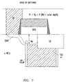
- the depletion region extends under the silicon substrate surface 50 and must be deeper than the depth of the top edge of the isolation collar between the silicon substrate and the inner electrode Wd 400 (Fig. 7). There is no continuous electrical connection between the bitline contact and the inner trench electrode 500 under this bias condition, and the charge is stored in the capacitor. As it is with all single transistor DRAM cells, leakage from the capacitor can occur.
- the doping profile in the buried strap must be chosen such that it provides adequate low resistance between the bitline contact and the conductive plate inside the trench. At the same time, the doping concentration must be sufficiently low to ensure that the majority carriers between the silicon interface with the gate dielectric and the top of the collar can be completely depleted at a voltage that does not damage the gate dielectric.
- the doping profile in the buried strap must be chosen to provide adequately low resistance between the bitline contact and the conductive plate within the trench when the device is switched on. At the same time, the doping profile must be low enough to ensure that majority carriers between the gate dielectric and below the top of the collar can be completely depleted at a suitable voltage selected such that it does not damage the gate dielectric when the device is switched off.
- the buried strap doping can be p-type or n-type. Further, the doping profile can be non-uniform and tailored to optimize the performance of the cell. The doping range would typically vary between 1e17/cm 3 and 1e19/cm 3 .
- a second embodiment for a uniformly doped buried strap and 6nm silicon dioxide is 3e17/cm 3 giving a strap resistance of 0.03 ⁇ -cm, a buried strap resistance in the silicon on top of the collar oxide of 3000 ⁇ , a device threshold voltage of -1.0 V, and a maximum depletion width of 39 nm.
- the doping profile can be non-uniform and tailored to optimize the performance of the cell. The doping range typically varies between 1e17/cm -3 to 1e19/cm -3 .
- the described depletion transfer device includes a gate overlapping or positioned directly over the trench capacitor.
- the buried strap connection between the trench capacitor and the bitline contact is provided in regions where the deep trench (DT) pattern intersects the active area (AA) of the device, and the upper section of the trench contains a single crystalline material in order to minimize the amount of leakage.
- the described structure and the process for fabricating the structure enable the trench storage capacitor and the array pass transistor to be formed directly on top or overlapping the buried strap to permit a reduction in the DRAM array cell area.
Applications Claiming Priority (2)
| Application Number | Priority Date | Filing Date | Title |
|---|---|---|---|
| US183306 | 1998-10-30 | ||
| US09/183,306 US6180975B1 (en) | 1998-10-30 | 1998-10-30 | Depletion strap semiconductor memory device |
Publications (2)
| Publication Number | Publication Date |
|---|---|
| EP0997947A1 true EP0997947A1 (fr) | 2000-05-03 |
| EP0997947B1 EP0997947B1 (fr) | 2008-09-03 |
Family
ID=22672265
Family Applications (1)
| Application Number | Title | Priority Date | Filing Date |
|---|---|---|---|
| EP99308160A Expired - Lifetime EP0997947B1 (fr) | 1998-10-30 | 1999-10-15 | Cellule DRAM à condensateur ensillonné |
Country Status (6)
| Country | Link |
|---|---|
| US (1) | US6180975B1 (fr) |
| EP (1) | EP0997947B1 (fr) |
| JP (1) | JP3408212B2 (fr) |
| KR (1) | KR100339185B1 (fr) |
| AT (1) | ATE407452T1 (fr) |
| DE (1) | DE69939451D1 (fr) |
Cited By (1)
| Publication number | Priority date | Publication date | Assignee | Title |
|---|---|---|---|---|
| WO2002073694A2 (fr) * | 2001-03-09 | 2002-09-19 | Infineon Technologies Ag | Cellule de memoire pourvue d'une tranchee et procede de fabrication |
Families Citing this family (10)
| Publication number | Priority date | Publication date | Assignee | Title |
|---|---|---|---|---|
| JP4381526B2 (ja) * | 1999-10-26 | 2009-12-09 | 東京エレクトロン株式会社 | プラズマエッチング方法 |
| US6316805B1 (en) * | 2000-01-06 | 2001-11-13 | Vanguard International Semiconductor Corporation | Electrostatic discharge device with gate-controlled field oxide transistor |
| DE10111755C1 (de) * | 2001-03-12 | 2002-05-16 | Infineon Technologies Ag | Verfahren zur Herstellung einer Speicherzelle eines Halbleiterspeichers |
| US6528367B1 (en) | 2001-11-30 | 2003-03-04 | Promos Technologies, Inc. | Self-aligned active array along the length direction to form un-biased buried strap formation for sub-150 NM BEST DRAM devices |
| US6979851B2 (en) * | 2002-10-04 | 2005-12-27 | International Business Machines Corporation | Structure and method of vertical transistor DRAM cell having a low leakage buried strap |
| DE102004012629B4 (de) * | 2004-03-16 | 2010-07-29 | Qimonda Ag | Speicherbauelement mit einem Feldeffekt-Halbleiterschalter und Verfahren zu seiner Herstellung |
| US7385234B2 (en) * | 2005-04-27 | 2008-06-10 | International Business Machines Corporation | Memory and logic devices using electronically scannable multiplexing devices |
| US7352029B2 (en) | 2005-04-27 | 2008-04-01 | International Business Machines Corporation | Electronically scannable multiplexing device |
| US7898014B2 (en) * | 2006-03-30 | 2011-03-01 | International Business Machines Corporation | Semiconductor device structures with self-aligned doped regions and methods for forming such semiconductor device structures |
| US20080048186A1 (en) * | 2006-03-30 | 2008-02-28 | International Business Machines Corporation | Design Structures Incorporating Semiconductor Device Structures with Self-Aligned Doped Regions |
Citations (6)
| Publication number | Priority date | Publication date | Assignee | Title |
|---|---|---|---|---|
| EP0187237A2 (fr) * | 1984-12-07 | 1986-07-16 | Texas Instruments Incorporated | Cellule dRAM et procédé |
| US4907047A (en) * | 1985-08-09 | 1990-03-06 | Nec Corporation | Semiconductor memory device |
| JPH04354367A (ja) * | 1991-05-31 | 1992-12-08 | Sony Corp | 半導体メモリ |
| JPH05160408A (ja) * | 1991-12-04 | 1993-06-25 | Toshiba Corp | 電界効果トランジスタおよびこれを用いたダイナミック型半導体記憶装置 |
| EP0713253A1 (fr) * | 1994-11-15 | 1996-05-22 | Siemens Aktiengesellschaft | Cellule DRAM à capacité ensillonée |
| JPH1093047A (ja) * | 1996-09-17 | 1998-04-10 | Toshiba Corp | 半導体記憶装置およびその製造方法 |
Family Cites Families (9)
| Publication number | Priority date | Publication date | Assignee | Title |
|---|---|---|---|---|
| US3986180A (en) | 1975-09-22 | 1976-10-12 | International Business Machines Corporation | Depletion mode field effect transistor memory system |
| US4389705A (en) | 1981-08-21 | 1983-06-21 | Mostek Corporation | Semiconductor memory circuit with depletion data transfer transistor |
| JPH0666443B2 (ja) | 1988-07-07 | 1994-08-24 | 株式会社東芝 | 半導体メモリセルおよび半導体メモリ |
| US5321285A (en) | 1990-05-07 | 1994-06-14 | Micron Technology, Inc. | Carrier injection dynamic random access memory having stacked depletion region in Mesa |
| US5198995A (en) | 1990-10-30 | 1993-03-30 | International Business Machines Corporation | Trench-capacitor-one-transistor storage cell and array for dynamic random access memories |
| JPH06333386A (ja) | 1993-05-20 | 1994-12-02 | Fujitsu Ltd | 半導体記憶装置 |
| DE4437261C1 (de) * | 1994-10-18 | 1995-10-19 | Siemens Ag | Mikromechanisches elektrostatisches Relais |
| JP2582535B2 (ja) | 1994-10-28 | 1997-02-19 | 九州日本電気株式会社 | 半導体装置 |
| US5998821A (en) * | 1997-05-21 | 1999-12-07 | Kabushiki Kaisha Toshiba | Dynamic ram structure having a trench capacitor |
-
1998
- 1998-10-30 US US09/183,306 patent/US6180975B1/en not_active Expired - Fee Related
-
1999
- 1999-09-10 KR KR1019990038565A patent/KR100339185B1/ko not_active IP Right Cessation
- 1999-10-13 JP JP29115799A patent/JP3408212B2/ja not_active Expired - Fee Related
- 1999-10-15 DE DE69939451T patent/DE69939451D1/de not_active Expired - Lifetime
- 1999-10-15 EP EP99308160A patent/EP0997947B1/fr not_active Expired - Lifetime
- 1999-10-15 AT AT99308160T patent/ATE407452T1/de not_active IP Right Cessation
Patent Citations (6)
| Publication number | Priority date | Publication date | Assignee | Title |
|---|---|---|---|---|
| EP0187237A2 (fr) * | 1984-12-07 | 1986-07-16 | Texas Instruments Incorporated | Cellule dRAM et procédé |
| US4907047A (en) * | 1985-08-09 | 1990-03-06 | Nec Corporation | Semiconductor memory device |
| JPH04354367A (ja) * | 1991-05-31 | 1992-12-08 | Sony Corp | 半導体メモリ |
| JPH05160408A (ja) * | 1991-12-04 | 1993-06-25 | Toshiba Corp | 電界効果トランジスタおよびこれを用いたダイナミック型半導体記憶装置 |
| EP0713253A1 (fr) * | 1994-11-15 | 1996-05-22 | Siemens Aktiengesellschaft | Cellule DRAM à capacité ensillonée |
| JPH1093047A (ja) * | 1996-09-17 | 1998-04-10 | Toshiba Corp | 半導体記憶装置およびその製造方法 |
Non-Patent Citations (3)
| Title |
|---|
| PATENT ABSTRACTS OF JAPAN vol. 17, no. 219 (E - 1358) 30 April 1993 (1993-04-30) * |
| PATENT ABSTRACTS OF JAPAN vol. 17, no. 556 (E - 1444) 6 October 1993 (1993-10-06) * |
| PATENT ABSTRACTS OF JAPAN vol. 1998, no. 9 31 July 1998 (1998-07-31) * |
Cited By (3)
| Publication number | Priority date | Publication date | Assignee | Title |
|---|---|---|---|---|
| WO2002073694A2 (fr) * | 2001-03-09 | 2002-09-19 | Infineon Technologies Ag | Cellule de memoire pourvue d'une tranchee et procede de fabrication |
| WO2002073694A3 (fr) * | 2001-03-09 | 2003-02-06 | Infineon Technologies Ag | Cellule de memoire pourvue d'une tranchee et procede de fabrication |
| US7067372B2 (en) | 2001-03-09 | 2006-06-27 | Infineon Technologies Ag | Method for fabricating a memory cell having a trench |
Also Published As
| Publication number | Publication date |
|---|---|
| KR100339185B1 (ko) | 2002-05-31 |
| KR20000028652A (ko) | 2000-05-25 |
| ATE407452T1 (de) | 2008-09-15 |
| JP2000138354A (ja) | 2000-05-16 |
| US6180975B1 (en) | 2001-01-30 |
| DE69939451D1 (de) | 2008-10-16 |
| JP3408212B2 (ja) | 2003-05-19 |
| EP0997947B1 (fr) | 2008-09-03 |
Similar Documents
| Publication | Publication Date | Title |
|---|---|---|
| US5937296A (en) | Memory cell that includes a vertical transistor and a trench capacitor | |
| KR100299342B1 (ko) | 반도체디바이스및그제조방법 | |
| US6204140B1 (en) | Dynamic random access memory | |
| CN100593860C (zh) | 具有凹陷通道晶体管的半导体器件 | |
| CN100536141C (zh) | 具有鳍形沟道晶体管的半导体器件及其制造方法 | |
| US6437388B1 (en) | Compact trench capacitor memory cell with body contact | |
| US6509599B1 (en) | Trench capacitor with insulation collar and method for producing the trench capacitor | |
| US6437401B1 (en) | Structure and method for improved isolation in trench storage cells | |
| EP1017095A2 (fr) | Cellule DRAM à condensateur ensillonné | |
| US6309924B1 (en) | Method of forming self-limiting polysilicon LOCOS for DRAM cell | |
| EP1396032A1 (fr) | Structure et procede permettant de former un contact corporel pour des cellules de transistor verticales | |
| WO2001091180A2 (fr) | Systeme et procede de formation d'un dispositif a orientation verticale dans un circuit integre | |
| US20080111194A1 (en) | Semiconductor device including a finfet | |
| KR100486190B1 (ko) | 다이내믹랜덤액세스메모리(dram)용메모리셀 | |
| EP0997947B1 (fr) | Cellule DRAM à condensateur ensillonné | |
| US20020127796A1 (en) | Method for producing a cell of a semiconductor memory | |
| US6872629B2 (en) | Method of forming a memory cell with a single sided buried strap | |
| US20020089007A1 (en) | Vertical mosfet | |
| US20230020711A1 (en) | Semiconductor structure and method for manufacturing same | |
| US11967626B2 (en) | Field effect transistors with gate fins and method of making the same | |
| TWI831396B (zh) | 製造記憶單元之方法 | |
| US6703274B1 (en) | Buried strap with limited outdiffusion and vertical transistor DRAM | |
| KR20070114463A (ko) | 자기 정렬 콘택 플러그를 구비한 반도체 소자 및 그제조방법 | |
| US20080237681A1 (en) | Semiconductor device and manufacturing method thereof | |
| EP0905772A2 (fr) | Cellule DRAM avec capacité ensillonée et son procédé de fabrication |
Legal Events
| Date | Code | Title | Description |
|---|---|---|---|
| PUAI | Public reference made under article 153(3) epc to a published international application that has entered the european phase |
Free format text: ORIGINAL CODE: 0009012 |
|
| AK | Designated contracting states |
Kind code of ref document: A1 Designated state(s): AT BE CH CY DE DK ES FI FR GB GR IE IT LI LU MC NL PT SE |
|
| AX | Request for extension of the european patent |
Free format text: AL;LT;LV;MK;RO;SI |
|
| 17P | Request for examination filed |
Effective date: 20000823 |
|
| AKX | Designation fees paid |
Free format text: AT BE CH CY DE DK ES FI FR GB GR IE IT LI LU MC NL PT SE |
|
| 17Q | First examination report despatched |
Effective date: 20070206 |
|
| GRAP | Despatch of communication of intention to grant a patent |
Free format text: ORIGINAL CODE: EPIDOSNIGR1 |
|
| GRAS | Grant fee paid |
Free format text: ORIGINAL CODE: EPIDOSNIGR3 |
|
| GRAA | (expected) grant |
Free format text: ORIGINAL CODE: 0009210 |
|
| AK | Designated contracting states |
Kind code of ref document: B1 Designated state(s): AT BE CH CY DE DK ES FI FR GB GR IE IT LI LU MC NL PT SE |
|
| REG | Reference to a national code |
Ref country code: GB Ref legal event code: FG4D |
|
| REG | Reference to a national code |
Ref country code: CH Ref legal event code: NV Representative=s name: IBM RESEARCH GMBH ZURICH RESEARCH LABORATORY INTEL Ref country code: CH Ref legal event code: EP |
|
| REG | Reference to a national code |
Ref country code: IE Ref legal event code: FG4D Ref country code: GB Ref legal event code: 746 Effective date: 20080909 |
|
| REF | Corresponds to: |
Ref document number: 69939451 Country of ref document: DE Date of ref document: 20081016 Kind code of ref document: P |
|
| PG25 | Lapsed in a contracting state [announced via postgrant information from national office to epo] |
Ref country code: NL Free format text: LAPSE BECAUSE OF FAILURE TO SUBMIT A TRANSLATION OF THE DESCRIPTION OR TO PAY THE FEE WITHIN THE PRESCRIBED TIME-LIMIT Effective date: 20080903 Ref country code: ES Free format text: LAPSE BECAUSE OF FAILURE TO SUBMIT A TRANSLATION OF THE DESCRIPTION OR TO PAY THE FEE WITHIN THE PRESCRIBED TIME-LIMIT Effective date: 20081214 |
|
| PG25 | Lapsed in a contracting state [announced via postgrant information from national office to epo] |
Ref country code: FI Free format text: LAPSE BECAUSE OF FAILURE TO SUBMIT A TRANSLATION OF THE DESCRIPTION OR TO PAY THE FEE WITHIN THE PRESCRIBED TIME-LIMIT Effective date: 20080903 Ref country code: AT Free format text: LAPSE BECAUSE OF FAILURE TO SUBMIT A TRANSLATION OF THE DESCRIPTION OR TO PAY THE FEE WITHIN THE PRESCRIBED TIME-LIMIT Effective date: 20080903 |
|
| NLV1 | Nl: lapsed or annulled due to failure to fulfill the requirements of art. 29p and 29m of the patents act | ||
| PG25 | Lapsed in a contracting state [announced via postgrant information from national office to epo] |
Ref country code: BE Free format text: LAPSE BECAUSE OF FAILURE TO SUBMIT A TRANSLATION OF THE DESCRIPTION OR TO PAY THE FEE WITHIN THE PRESCRIBED TIME-LIMIT Effective date: 20080903 |
|
| PG25 | Lapsed in a contracting state [announced via postgrant information from national office to epo] |
Ref country code: PT Free format text: LAPSE BECAUSE OF FAILURE TO SUBMIT A TRANSLATION OF THE DESCRIPTION OR TO PAY THE FEE WITHIN THE PRESCRIBED TIME-LIMIT Effective date: 20090203 Ref country code: MC Free format text: LAPSE BECAUSE OF NON-PAYMENT OF DUE FEES Effective date: 20081031 |
|
| REG | Reference to a national code |
Ref country code: CH Ref legal event code: PL |
|
| PLBE | No opposition filed within time limit |
Free format text: ORIGINAL CODE: 0009261 |
|
| STAA | Information on the status of an ep patent application or granted ep patent |
Free format text: STATUS: NO OPPOSITION FILED WITHIN TIME LIMIT |
|
| REG | Reference to a national code |
Ref country code: IE Ref legal event code: MM4A |
|
| PG25 | Lapsed in a contracting state [announced via postgrant information from national office to epo] |
Ref country code: DK Free format text: LAPSE BECAUSE OF FAILURE TO SUBMIT A TRANSLATION OF THE DESCRIPTION OR TO PAY THE FEE WITHIN THE PRESCRIBED TIME-LIMIT Effective date: 20080903 |
|
| 26N | No opposition filed |
Effective date: 20090604 |
|
| PG25 | Lapsed in a contracting state [announced via postgrant information from national office to epo] |
Ref country code: IT Free format text: LAPSE BECAUSE OF FAILURE TO SUBMIT A TRANSLATION OF THE DESCRIPTION OR TO PAY THE FEE WITHIN THE PRESCRIBED TIME-LIMIT Effective date: 20080903 |
|
| PG25 | Lapsed in a contracting state [announced via postgrant information from national office to epo] |
Ref country code: LI Free format text: LAPSE BECAUSE OF NON-PAYMENT OF DUE FEES Effective date: 20081031 Ref country code: IE Free format text: LAPSE BECAUSE OF NON-PAYMENT OF DUE FEES Effective date: 20081015 Ref country code: CH Free format text: LAPSE BECAUSE OF NON-PAYMENT OF DUE FEES Effective date: 20081031 |
|
| PG25 | Lapsed in a contracting state [announced via postgrant information from national office to epo] |
Ref country code: SE Free format text: LAPSE BECAUSE OF FAILURE TO SUBMIT A TRANSLATION OF THE DESCRIPTION OR TO PAY THE FEE WITHIN THE PRESCRIBED TIME-LIMIT Effective date: 20081203 |
|
| PG25 | Lapsed in a contracting state [announced via postgrant information from national office to epo] |
Ref country code: LU Free format text: LAPSE BECAUSE OF NON-PAYMENT OF DUE FEES Effective date: 20081015 |
|
| PG25 | Lapsed in a contracting state [announced via postgrant information from national office to epo] |
Ref country code: CY Free format text: LAPSE BECAUSE OF FAILURE TO SUBMIT A TRANSLATION OF THE DESCRIPTION OR TO PAY THE FEE WITHIN THE PRESCRIBED TIME-LIMIT Effective date: 20080903 |
|
| PG25 | Lapsed in a contracting state [announced via postgrant information from national office to epo] |
Ref country code: GR Free format text: LAPSE BECAUSE OF FAILURE TO SUBMIT A TRANSLATION OF THE DESCRIPTION OR TO PAY THE FEE WITHIN THE PRESCRIBED TIME-LIMIT Effective date: 20081204 |
|
| PGFP | Annual fee paid to national office [announced via postgrant information from national office to epo] |
Ref country code: FR Payment date: 20101018 Year of fee payment: 12 |
|
| PGFP | Annual fee paid to national office [announced via postgrant information from national office to epo] |
Ref country code: DE Payment date: 20101028 Year of fee payment: 12 |
|
| PGFP | Annual fee paid to national office [announced via postgrant information from national office to epo] |
Ref country code: GB Payment date: 20101022 Year of fee payment: 12 |
|
| GBPC | Gb: european patent ceased through non-payment of renewal fee |
Effective date: 20111015 |
|
| REG | Reference to a national code |
Ref country code: FR Ref legal event code: ST Effective date: 20120629 |
|
| PG25 | Lapsed in a contracting state [announced via postgrant information from national office to epo] |
Ref country code: DE Free format text: LAPSE BECAUSE OF NON-PAYMENT OF DUE FEES Effective date: 20120501 |
|
| REG | Reference to a national code |
Ref country code: DE Ref legal event code: R119 Ref document number: 69939451 Country of ref document: DE Effective date: 20120501 |
|
| PG25 | Lapsed in a contracting state [announced via postgrant information from national office to epo] |
Ref country code: GB Free format text: LAPSE BECAUSE OF NON-PAYMENT OF DUE FEES Effective date: 20111015 Ref country code: FR Free format text: LAPSE BECAUSE OF NON-PAYMENT OF DUE FEES Effective date: 20111102 |