EP0987603A1 - Elektrophotographisches photoempfindliches Element und elektrophotographisches Gerät - Google Patents
Elektrophotographisches photoempfindliches Element und elektrophotographisches Gerät Download PDFInfo
- Publication number
- EP0987603A1 EP0987603A1 EP99118383A EP99118383A EP0987603A1 EP 0987603 A1 EP0987603 A1 EP 0987603A1 EP 99118383 A EP99118383 A EP 99118383A EP 99118383 A EP99118383 A EP 99118383A EP 0987603 A1 EP0987603 A1 EP 0987603A1
- Authority
- EP
- European Patent Office
- Prior art keywords
- photosensitive drum
- drum
- toner
- electrophotographic photosensitive
- electrophotographic
- Prior art date
- Legal status (The legal status is an assumption and is not a legal conclusion. Google has not performed a legal analysis and makes no representation as to the accuracy of the status listed.)
- Granted
Links
Images


Classifications
-
- G—PHYSICS
- G03—PHOTOGRAPHY; CINEMATOGRAPHY; ANALOGOUS TECHNIQUES USING WAVES OTHER THAN OPTICAL WAVES; ELECTROGRAPHY; HOLOGRAPHY
- G03G—ELECTROGRAPHY; ELECTROPHOTOGRAPHY; MAGNETOGRAPHY
- G03G5/00—Recording members for original recording by exposure, e.g. to light, to heat, to electrons; Manufacture thereof; Selection of materials therefor
- G03G5/02—Charge-receiving layers
- G03G5/04—Photoconductive layers; Charge-generation layers or charge-transporting layers; Additives therefor; Binders therefor
- G03G5/08—Photoconductive layers; Charge-generation layers or charge-transporting layers; Additives therefor; Binders therefor characterised by the photoconductive material being inorganic
- G03G5/082—Photoconductive layers; Charge-generation layers or charge-transporting layers; Additives therefor; Binders therefor characterised by the photoconductive material being inorganic and not being incorporated in a bonding material, e.g. vacuum deposited
- G03G5/08214—Silicon-based
- G03G5/08221—Silicon-based comprising one or two silicon based layers
-
- G—PHYSICS
- G03—PHOTOGRAPHY; CINEMATOGRAPHY; ANALOGOUS TECHNIQUES USING WAVES OTHER THAN OPTICAL WAVES; ELECTROGRAPHY; HOLOGRAPHY
- G03G—ELECTROGRAPHY; ELECTROPHOTOGRAPHY; MAGNETOGRAPHY
- G03G5/00—Recording members for original recording by exposure, e.g. to light, to heat, to electrons; Manufacture thereof; Selection of materials therefor
- G03G5/02—Charge-receiving layers
-
- G—PHYSICS
- G03—PHOTOGRAPHY; CINEMATOGRAPHY; ANALOGOUS TECHNIQUES USING WAVES OTHER THAN OPTICAL WAVES; ELECTROGRAPHY; HOLOGRAPHY
- G03G—ELECTROGRAPHY; ELECTROPHOTOGRAPHY; MAGNETOGRAPHY
- G03G5/00—Recording members for original recording by exposure, e.g. to light, to heat, to electrons; Manufacture thereof; Selection of materials therefor
- G03G5/10—Bases for charge-receiving or other layers
-
- G—PHYSICS
- G03—PHOTOGRAPHY; CINEMATOGRAPHY; ANALOGOUS TECHNIQUES USING WAVES OTHER THAN OPTICAL WAVES; ELECTROGRAPHY; HOLOGRAPHY
- G03G—ELECTROGRAPHY; ELECTROPHOTOGRAPHY; MAGNETOGRAPHY
- G03G5/00—Recording members for original recording by exposure, e.g. to light, to heat, to electrons; Manufacture thereof; Selection of materials therefor
- G03G5/14—Inert intermediate or cover layers for charge-receiving layers
Definitions
- the present invention relates to an electrophotographic photosensitive member provided with a photosensitive layer containing at least amorphous silicon (hereinafter referred to as a-Si) on a cylindrical conductive substrate, as well as to an image forming apparatus provided with the electrophotographic sensitive member, such as a copying machine, a printer, that forms images utilizing the electrophotographic process.
- a-Si amorphous silicon
- a conventional image forming apparatus such as a copying machine, a printer, a facsimile apparatus, utilizing the electrophotographic process, is arranged to form images by a charging process to charge the electrophotographic photosensitive drum (hereinafter referred to as a photosensitive drum) evenly and uniformly, which serves as an image bearing member in general; by a latent image forming process to write electrostatic latent images on the photosensitive drum; by a developing process to develop the electrostatic latent image with toner (developer); by a transfer process to transfer toner on the photosensitive drum to a transfer material; and by a fixing process to fix the toner on the transfer material.
- a charging process to charge the electrophotographic photosensitive drum (hereinafter referred to as a photosensitive drum) evenly and uniformly, which serves as an image bearing member in general
- a latent image forming process to write electrostatic latent images on the photosensitive drum
- developing process to develop the electrostatic latent image with toner (developer)
- developer toner
- transfer process
- the residual toner which remains on the photosensitive drum is removed by use of a cleaning device.
- the cleaning device that removes the residual toner remaining on the photosensitive drum after transfer
- various ones have been proposed conventionally.
- the cleaning device which scrapes off the residual toner remaining on the photosensitive drum after transfer by the cleaning blade formed by urethane rubber or some other elastic material, and which is widely in use because this device presents an excellent function of toner removal, while it can be structured compactly at lower costs.
- the particles, which adhere to the surface of the photosensitive drum to affect the image quality are not only the toner, but also, the fine paper particles created from paper used for most of the transfer materials, the organic component extracted from the fine paper particles, and the corona product created due to the presence of the high-voltage member in the apparatus, among some others. If these particles as foreign substances should adhere to the surface of the photosensitive drum, it tends to impede the formation of clear electrostatic latent images, because these foreign substances present lower resistance condition under high humidity environment, thus inviting the degradation of image quality eventually.
- the a-Si photosensitive drum that forms film by the glow discharge decomposition of silane is easier to be affected by the above-mentioned phenomenon that may lead to the image degradation.
- a method has been proposed to rub and remove the various foreign substances described above by the grinding function of toner particles in the location of the cleaning blade in such a manner that when the magnetic toner of monocomponent type is used as the developer in particular, the magnetic roller is arranged on the upstream side of the cleaning blade in a running direction (rotational direction) of the photosensitive drum so as to form the magnetic brush by use of a part of the toner (residual toner after transfer) collected by the cleaning blade, and that the magnetic brush thus formed is in contact with the surface of the photosensitive drum to supply the magnetic toner again.
- the above-mentioned method has a lesser degree of the grinding function biased toward the surface of the photosensitive drum. Then, it may be possible to apply this method to the so-called Carlson photosensitive drum which enables charges to be transported in the photosensitive layer of the photosensitive drum at the time of exposure.
- this method produces a specific effect on the prevention of the image degradation resulting from the causes described above when it is used in combination with a method in which the surface of the photosensitive drum is prevented from presenting the lower resistance with the arrangement of a heater for the photosensitive drum, for example, so as to make humidity lower on the circumference of the drum at night or during standby.
- the contact pressure of the cleaning blade becomes higher inevitably. Further, on both ends of the cleaning blade, toner is not supplied to the magnet roller sufficiently. The resultant coating amount of toner becomes smaller, and in some cases, the toner is not supplied to the cleaning blade sufficiently. Under such condition, the cleaning blade is allowed to vibrate on both ends thereof in particular, making it impossible to remove toner on the surface of the photosensitive drum completely to result in the defective cleaning.
- the present invention is designed to provide an electrophotographic amorphous silicon photosensitive member used for an electrophotographic apparatus that forms images by the electrophotographic method, and an image forming apparatus that uses this photosensitive member, and comprises a drum-shaped cylindrical conductive substrate, and a photosensitive layer that contains amorphous silicon and that is provided on the drum-shaped cylindrical conductive substrate, thus structuring an electro-photographic photosensitive drum.
- the outer diameter of this photosensitive drum is configured to be gradually smaller from the vicinity of the central portion thereof in the generatrix direction to both ends in the longitudinal direction, hence making it possible to enhance the cleaning effect on residual toner.
- Fig. 1 is a structural view which schematically shows an image forming apparatus provided with a photosensitive drum in accordance with the present embodiment.
- the image forming apparatus shown in Fig. 1 is provided with the photosensitive drum 1 as image bearing member to be driven to rotate in the direction indicated by an arrow R1.
- a pre-exposure device 2 On the circumference of the photosensitive drum 1, there are provided a pre-exposure device 2; a primary charger 3; a developing device 4; a post charger 5; a transfer and separation charger 6; and a cleaning device 7.
- a transfer material P such as a paper sheet
- a resistration roller 8 a conveying device 9, and a fixing device 10 are arranged from the upstream side in that order with the photosensitive drum 1 between them.
- the photosensitive drum 1 is provided with the a-Si photosensitive layer in a thickness of approximately 30 ⁇ m on a cylindrical substrate formed by metal (aluminum, for example) in a thickness of approximately 5 mm, and the outer diameter thereof is formed in 108 mm.
- the photosensitive drum 1 is driven by driving means (not shown) at a specific speed in the direction indicated by the arrow R1.
- the surface of the photosensitive drum 1 is uniformly charged by a glow discharge of the primary charger 3.
- a sheet heater 11 of approximately 80W is arranged around it. The electric power is controlled so that the temperature of the drum substrate is kept at approximately 42°C.
- the photosensitive drum 1 is configured in the inverted crown shape as shown in Figs. 2A and 2B (the detailed structure of the photosensitive drum 1 will be described later).
- the developing device 4 is provided with a developing sleeve 12 formed by a coating layer of the mixture of phenol resin, graphite, and carbon on the surface of aluminum cylinder of 20 mm diameter in the present embodiment, and then, the toner t which is the developer is contained in the developing device 4.
- the toner t is coated on the developing sleeve 12 by a magnetic blade (not shown).
- a gap of approximately 280 ⁇ m is set between the developing sleeve 12 and the magnetic blade (not shown).
- the monocomponent magnetic toner whose glass-transition temperature is approximately 60°C is used.
- the toner has an average particle diameter of approximately 9 ⁇ m and is negatively charged.
- the styrene acril is used as the main binder.
- the magnetic member of approximately 80 parts by weights is used. 4 % strontium titanate and 0.5 % silica are used as the external additives to it.
- the triboelectricity of the toner t is -3 to 12 ( ⁇ C/g) on the developing sleeve 12, and the coating amount is 0.6 to 1.3 mg/cm 2 .
- the developing sleeve 12 is driven in the direction opposite to the rotational direction of the photosensitive drum 1 at a relative speed of 150%.
- the gap is set at approximately 230 ⁇ m between the developing sleeve 12 and the photosensitive drum 1.
- the developing bias is applied from a high-voltage supply source (not shown) at the frequency of 2,700 Hz and the peak-to-peak voltage of 1,400 V with the superposition of the direct current and the rectangular waves of 35% duty ratio.
- the cleaning device 7 is provided with the cleaning blade 17 to remove the residual toner after transfer which remains on the surface of the photosensitive drum 1 subsequent to the execution of the transfer.
- the fixing device 10 is provided with the fixing roller 13 and the pressure roller 14.
- the fixing roller 13 and the pressure roller 14 are in pressure contact with each other.
- the fluoroplastic (PTFE) surface layer is coated by burning in a thickness of approximately 20 ⁇ m on the silicon rubber layer of 0.25 mm thick.
- the pressure roller 14 is formed by the silicon rubber of 60 mm diameter and 5 mm thick, which is covered by the fluoroplastic (PFA) tube of 100 ⁇ m thick.
- the halogen heater 15 of rated 1,600 W is arranged.
- a high-voltage supply source and others are connected to the primary charger 3, the developing sleeve 12, and the transfer and separation charger 6.
- each of the photosensitive drum 1, the developing sleeve 12, and the fixing roller 13 is provided with a driving motor (not shown), respectively, so as to enable each of them to be driven to rotate individually.
- the photosensitive drum 1 is driven by driving means (not shown) to rotate in the direction indicated by the arrow R1 at a predetermined speed. After the residual charge of the surface thereof is eliminated by the pre-exposure device 2, the surface is uniformly charged by the primary charger 3. Then, the image exposure L is effectuated on the surface of the photosensitive drum 1 in accordance with image information inputted from the exposing device (not shown) so that the charges on the exposed portions are eliminated to form an electrostatic latent image.
- the electrostatic latent image is developed by the adhesion of toner by the developing sleeve 12 of the developing device 4, to which the developing bias has been applied accordingly, hence being visualized as toner images.
- the transfer material P which has been conveyed by a conveying system (not shown), is fed by the resistration roller 8 in sync with the timing.
- the transfer and separation charger 6 to which the transfer bias is applied the toner image on the photosensitive drum 1 is transferred to the surface of the transfer material P.
- the transfer material P which has been separated from the photosensitive drum 1 by the function of the transfer and separation charger 6, is conveyed by the conveying device 9 to the gap between the fixing roller 13 and the pressure roller 14 of the fixing device 10.
- the transfer material P having the toner image thus transferred is discharged to the outside after the toner image is fixed by the pressure and heating between the fixing roller 13 heated by the halogen heater 15 and the pressure roller 14.
- the residual toner remaining on the photosensitive drum 1 is removed by the cleaning device 7.
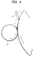
- the cleaning blade 17 is held to abut against the surface of the photosensitive drum 1 as shown in Fig. 3.
- the magnet roller 18 is provided to form a predetermined gap between the photosensitive drum 1 and the magnet roller 18 in the longitudinal direction of the photosensitive drum 1.
- the cleaning blade 17 is formed by urethane rubber of 2 mm in thickness, and the magnet roller 18 is structured by a roller of 18 mm in diameter which is provided with eight poles each having the magnetic-flux density of 500 gauss.
- the toner layer thickness regulating roller 19 of a smaller diameter (8 mm in diameter), which regulates the thickness of the toner layer formed on the surface of the magnet roller 18, is arranged rotatably in parallel with the magnet roller 18. Then, the scraper 21 installed on the distal end of the stay 20, the other end of which is fixed to the cleaning container 16, is in contact with the surface of the toner layer thickness regulating roller 19. Also, on the bottom in the cleaning container 16, a conveying screw 22 is rotatably arranged in the longitudinal direction of the magnet roller 18.
- the toner layer thickness regulating roller 19 is structured by non-magnetic material. On the surface of the toner layer thickness regulating roller 19, the fluoroplastic which is a substance having a smaller surface energy is coated in a thickness of approximately 10 to 50 ⁇ m.
- the magnet roller 18 is driven by driving means (not shown) to rotate in clockwise direction with respect to the photosensitive drum 1 at a speed slower than the rotation of the photosensitive drum 1.
- the toner layer thickness regulating roller 19 is driven to rotate in the direction (counterclockwise direction) opposite to that of the magnet roller 18 at a predetermined speed.
- the residual toner t' after transfer which remains on the photosensitive drum 1 without being transferred to the transfer material P is scraped off from the photosensitive drum 1 by the cleaning blade 17 when the residual toner arrives at the position of the cleaning device 7 from the transfer nip (the position between the photosensitive drum 1 and the transfer and separation charger 6) along with the rotation of the photosensitive drum 1.
- the residual toner t' after transfer thus scraped off drops onto the magnet roller 18, and forms the toner gathering between the magnet roller 18 and the photosensitive drum 1.
- the residual toner on the photosensitive drum 1 is adsorbed to the magnet roller 18 and conveyed to form the toner layer on the magnet roller 18.
- This toner layer is regulated to an even thickness by the toner layer thickness regulating roller 19.
- the residual toner t' after transfer on the magnet roller 18 is caused to stand like the ears of rice to form a magnetic brush on the surface of the magnet roller 18.
- the brush reaches the location opposite to the photosensitive drum 1 one after another so as to operate the rub cleaning for the removal of various foreign substances adhering to the surface of the photosensitive drum 1.
- the residual toner t' after transfer which has overflown from the toner layer thickness regulating roller 19 is conveyed by the conveying screw 22 in the depth direction of the interior of the cleaning container 16, hence being collected into a waste toner container (not shown).
- toner is coated evenly on the surface of the photosensitive drum 1 by the standing magnetic brush on the surface of the magnet roller 18.
- the toner thus coated evenly on the surface of the photosensitive drum 1 is either scraped off by the cleaning blade 17 or resides on the cleaning blade 17 to perform the rub cleaning for the photosensitive drum 1 together with the cleaning blade 17.
- the photosensitive drum 1 comprises a drum-shaped metallic substrate, and the photoconductive layer formed on the substrate, which contains an amorphous material having silicon atom as its matrix (preferably, an amorphous material containing at least either one of hydrogen atom and halogen atom as its component atom). Also, there is provided a barrier wall layer between the drum-shaped metallic substrate and the photoconductive layer, and an upper layer as the surface charge blocking layer or the protection layer is arranged on the photoconductive layer.
- the basic material used for the drum-shaped metallic substrate which is preferably adopted for the present invention is metal, such as NiCr, stainless steel, Al, Cr, Mo, Au, Nb, Ta, V, Ti, Pt, or Pd, or its alloy.
- Al and Al alloys are used preferably in particular.
- the reason why the Al and Al alloys are preferably used in particular for the drum-shaped metallic substrate is that it is comparatively easier to obtain the material having the exact circle and surface flatness and smoothness in good precision, and at the time of manufacture, it is easier to control the temperature on the deposition surface of the a-Si (H, X), and then, it is economical to use them.
- halogen atom (X) which may be contained in the photoconductive layer of the photosensitive drum 1
- fluorine chlorine, bromine, and iodine.
- chlorine and more preferably, fluorine.
- the third group atom such as boron, gallium, listed on the table of the periodic law
- the fifth group atom such as nitrogen, phosphorus, arsenic, listed on the table of the periodic law, or the oxygen atom, carbon atom, germanium atom, or the like may be contained individually or in an appropriate combination as the component that may adjust the Fermi level, the width of forbidden band, or the like.
- the barrier wall layer is arranged for the purpose to enhance the contactness between the photoconductive layer and the drum-shaped metallic substrate or to adjust the charge acceptance capacity.
- the barrier wall layer is structured as a monolayer or multiple layer with the a-Si (H, X) layer or polycrystal-Si layer containing the III group atom, V group atom, oxygen atom, carbon atom, germanium atom or the like depending on the intended purpose.
- a layer may be arranged as the surface charge blocking layer or the protection layer, which is formed by the amorphous material preferably containing a large amount of carbon atom, nitrogen atom, oxygen atom, or the like with the silicon atom as its matrix, which may also contain hydrogen atom or halogen atom as required, or a layer which is formed by highly resistive organic substance may also be arranged.
- the method of forming the photoconductive layer structured by the a-Si H, X
- the outer diameter of the photosensitive drum 1 of the present invention is made gradually smaller from the central position of the photosensitive drum 1 to both ends thereof in the generatrix direction (longitudinal direction) as shown in Figs. 2A and 2B.
- the shape of the photosensitive drum 1 is in the form of inverted crown.
- the print durability is set for 100,000 A4-sized sheets each in the case of the cleaning device 7 which is provided with the magnet roller 18 and the one which is provided only with the cleaning blade 17 but not with the magnet roller 18, and also, the evaluation is made as to the cleaning effect produced on the residual toner t' after transfer each with the solid white/half tone/solid black images, respectively.
- the durability is set under the environments of constant temperature/humidity (30°C/60%). The results of the evaluation are shown on Table 2: With Magnet Roller Without Magnet Roller Conventional drum Drum of the Invention
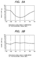
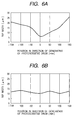
- Figs. 5A and 5B, and Figs. 6A and 6B are views which represent the relationships between the blade loads of the cleaning blade 17 and the nip widths in the longitudinal direction of the photosensitive drum on evaluating cleaning effects of the cleaning blade 17 for the residual toner t' after transfer.
- Fig. 5A shows the blade loads of the conventional photosensitive drum.
- Fig. 5B shows the blade loads of the invention.
- Fig. 6A shows the nip widths of the conventional photosensitive drum, and Fig. 6B shows the nip widths of the invention.
- the print durability is set for 100,000 A4-sized sheets, and then, the evaluation is made on the cleaning condition of the residual toner t' after transfer by the cleaning blade 17, the deflection widths of the blade loads of each photosensitive drums ((the maximum - the minimum) / the mean value), as well as on the uneven image densities of the half tone images.
- the durability is set under the environments of constant temperature/humidity (30°C/60%).
- the inverted crown type of the photosensitive drum 1 so that the ⁇ A (the outer diameter of the photosensitive drum 1 in the central position in the generatrix direction) - ⁇ B (the outer diameter of each end) becomes 60 to 100 ⁇ m for the present invention.
- the evaluation is made on the cleaning conditions by use of the photosensitive drum of the organic photosensitive member (OPC photosensitive member) of 108 mm in outer diameter as a comparative example used for the present invention. Then, during the durability observation, the surface of the photosensitive drum is ground and scratched. As a result, it becomes impossible to obtain good results.
- OPC photosensitive member organic photosensitive member
- the inverted crown type photosensitive drums 30 shown in Figs. 7A and 7B the evaluation is made on the cleaning conditions as described above.
- the photosensitive drum 30 shown in Fig. 7A is configured in the inverted crown shape, the ⁇ A (the outer diameter of the photosensitive drum 30 in the central position in the generatrix direction) - ⁇ B (the outer diameter on each end) of which is 200 ⁇ m or more.
- the photosensitive drum 30 shown in Fig. 7B is configured in the inverted crown shape having stepped portions in the generatrix direction (longitudinal direction) thereof.
- the shape of the photosensitive drum having the a-Si photosensitive layer is formed so that the outer diameter of the photosensitive drum is made gradually smaller in the longitudinal direction from the vicinity of the central position to the both ends, respectively.
- the nip widths of the cleaning blade which should abut against the photosensitive drum are uniformalized, and then, the abutting load of the cleaning blade becomes even accordingly.
- the cleaning blade it becomes possible for the cleaning blade to effectuate the uniform cleaning in the longitudinal direction so as to obtain clear and high quality images stably by preventing the images from running or the like even under a high humid environment, as well as to attain making the grinding amount of the a-Si photosensitive layer of the photosensitive drum even.
- An electrophotographic amorphous silicon photosensitive member is used for an electrophotographic apparatus that forms images by the electrophotographic method, and an image forming apparatus uses this photosensitive member, which includes a drum-shaped cylindrical conductive substrate, and a photosensitive layer that contains amorphous silicon, thus structuring an electrophotographic photosensitive drum. Then, the outer diameter of this photosensitive drum is configured to be gradually smaller from the vicinity of the central portion thereof in the generatrix direction to both ends in the longitudinal direction, hence making it possible to enhance the cleaning effect on residual toner.
Landscapes
- Physics & Mathematics (AREA)
- General Physics & Mathematics (AREA)
- Chemical & Material Sciences (AREA)
- Inorganic Chemistry (AREA)
- Cleaning In Electrography (AREA)
- Photoreceptors In Electrophotography (AREA)
Applications Claiming Priority (2)
| Application Number | Priority Date | Filing Date | Title |
|---|---|---|---|
| JP10263347A JP2000098642A (ja) | 1998-09-17 | 1998-09-17 | 電子写真感光ドラム及び画像形成装置 |
| JP26334798 | 1998-09-17 |
Publications (3)
| Publication Number | Publication Date |
|---|---|
| EP0987603A1 true EP0987603A1 (de) | 2000-03-22 |
| EP0987603B1 EP0987603B1 (de) | 2006-04-12 |
| EP0987603B8 EP0987603B8 (de) | 2006-08-16 |
Family
ID=17388218
Family Applications (1)
| Application Number | Title | Priority Date | Filing Date |
|---|---|---|---|
| EP99118383A Expired - Lifetime EP0987603B8 (de) | 1998-09-17 | 1999-09-16 | Elektrophotographisches photoempfindliches Element und elektrophotographisches Gerät |
Country Status (4)
| Country | Link |
|---|---|
| US (1) | US6226479B1 (de) |
| EP (1) | EP0987603B8 (de) |
| JP (1) | JP2000098642A (de) |
| DE (1) | DE69930808T2 (de) |
Families Citing this family (10)
| Publication number | Priority date | Publication date | Assignee | Title |
|---|---|---|---|---|
| WO2003007111A2 (en) * | 2001-07-09 | 2003-01-23 | Rochester Institute Of Technology | Wiper blade assessment system and a method thereof |
| JP4053010B2 (ja) * | 2004-02-24 | 2008-02-27 | 株式会社沖データ | 現像装置と現像装置を内蔵する画像形成装置 |
| US7623810B2 (en) * | 2005-10-28 | 2009-11-24 | Kyocera Corporation | Electrophotographic photosensitive member and image forming apparatus provided with the same |
| JP4242901B2 (ja) | 2006-02-24 | 2009-03-25 | 京セラ株式会社 | 画像形成装置 |
| JP4377923B2 (ja) | 2006-02-24 | 2009-12-02 | 京セラ株式会社 | 画像形成装置 |
| JP2007293280A (ja) | 2006-03-30 | 2007-11-08 | Kyocera Corp | 電子写真感光体およびこれを備えた画像形成装置 |
| JP2008058649A (ja) * | 2006-08-31 | 2008-03-13 | Kyocera Corp | 電子写真感光体およびこれを備えた画像形成装置 |
| US7962085B2 (en) * | 2009-10-15 | 2011-06-14 | Xerox Corporation | Metal blade cleaning of an amorphous silicon receptor |
| JP5266264B2 (ja) * | 2010-01-20 | 2013-08-21 | 京セラドキュメントソリューションズ株式会社 | クリーニング装置及び画像形成装置 |
| JP5523401B2 (ja) | 2010-07-05 | 2014-06-18 | キヤノン株式会社 | 画像形成方法 |
Citations (5)
| Publication number | Priority date | Publication date | Assignee | Title |
|---|---|---|---|---|
| US4045134A (en) * | 1975-03-05 | 1977-08-30 | Ricoh Company, Ltd. | Photosensitive member for use in electrophotographic apparatus and method of manufacturing the same |
| JPS62212663A (ja) * | 1986-03-14 | 1987-09-18 | Fuji Electric Co Ltd | 電子写真感光体 |
| JPH06337534A (ja) * | 1993-05-28 | 1994-12-06 | Kyocera Corp | 電子写真感光体の製法 |
| JPH08146632A (ja) * | 1994-11-22 | 1996-06-07 | Kyocera Corp | 電子写真感光体の製造方法 |
| JPH09297500A (ja) * | 1996-03-08 | 1997-11-18 | Canon Inc | 光受容部材、該光受容部材用基体及び該光受容部材を有する電子写真装置 |
Family Cites Families (3)
| Publication number | Priority date | Publication date | Assignee | Title |
|---|---|---|---|---|
| US3984183A (en) * | 1975-02-24 | 1976-10-05 | Xerox Corporation | Sheet stripping from imaging surface |
| EP0458273B1 (de) * | 1990-05-21 | 1997-08-13 | Canon Kabushiki Kaisha | Aufladevorrichtung, Bilderzeugungsgerät mit einer solchen Vorrichtung und von dem Bilderzeugungsgerät abnehmbare Arbeitseinheit |
| DE69512575T2 (de) * | 1994-07-06 | 2000-05-04 | Canon Kk | Elektrografisches Gerät und Bilderzeugungsverfahren |
-
1998
- 1998-09-17 JP JP10263347A patent/JP2000098642A/ja active Pending
-
1999
- 1999-09-16 EP EP99118383A patent/EP0987603B8/de not_active Expired - Lifetime
- 1999-09-16 DE DE69930808T patent/DE69930808T2/de not_active Expired - Lifetime
- 1999-09-16 US US09/391,047 patent/US6226479B1/en not_active Expired - Lifetime
Patent Citations (6)
| Publication number | Priority date | Publication date | Assignee | Title |
|---|---|---|---|---|
| US4045134A (en) * | 1975-03-05 | 1977-08-30 | Ricoh Company, Ltd. | Photosensitive member for use in electrophotographic apparatus and method of manufacturing the same |
| JPS62212663A (ja) * | 1986-03-14 | 1987-09-18 | Fuji Electric Co Ltd | 電子写真感光体 |
| JPH06337534A (ja) * | 1993-05-28 | 1994-12-06 | Kyocera Corp | 電子写真感光体の製法 |
| JPH08146632A (ja) * | 1994-11-22 | 1996-06-07 | Kyocera Corp | 電子写真感光体の製造方法 |
| JPH09297500A (ja) * | 1996-03-08 | 1997-11-18 | Canon Inc | 光受容部材、該光受容部材用基体及び該光受容部材を有する電子写真装置 |
| US5853936A (en) * | 1996-03-08 | 1998-12-29 | Canon Kabushiki Kaisha | Light receiving member, substrate for said light receiving member, and electrophotographic apparatus having said light receiving member |
Non-Patent Citations (5)
| Title |
|---|
| DATABASE WPI Week 9633, Derwent World Patents Index; AN 1996-325058, XP002124100 * |
| DATABASE WPI Week 9805, Derwent World Patents Index; AN 1998-048326, XP002124099 * |
| PATENT ABSTRACTS OF JAPAN vol. 12, no. 74 (P - 674) 9 March 1988 (1988-03-09) * |
| PATENT ABSTRACTS OF JAPAN vol. 1995, no. 03 28 April 1995 (1995-04-28) * |
| PATENT ABSTRACTS OF JAPAN vol. 1996, no. 10 31 October 1996 (1996-10-31) * |
Also Published As
| Publication number | Publication date |
|---|---|
| DE69930808T2 (de) | 2006-10-19 |
| EP0987603B8 (de) | 2006-08-16 |
| US6226479B1 (en) | 2001-05-01 |
| JP2000098642A (ja) | 2000-04-07 |
| EP0987603B1 (de) | 2006-04-12 |
| DE69930808D1 (de) | 2006-05-24 |
Similar Documents
| Publication | Publication Date | Title |
|---|---|---|
| US7778573B2 (en) | Image forming apparatus and process cartridge | |
| US5459558A (en) | Charging device, image forming apparatus with same and a process unit detachably mountable to the image forming apparatus | |
| JP2003156971A (ja) | 画像形成装置 | |
| US6226479B1 (en) | Electrophotographic photosensitive member and image forming apparatus | |
| JP4467944B2 (ja) | 現像剤担持体及び現像装置 | |
| US6269235B1 (en) | Developing apparatus featuring first and second developer bearing members each including a non-negative member and a coating member covering the non-negative member | |
| JP2005055837A (ja) | 画像形成装置における現像方法及び装置 | |
| US6868240B2 (en) | Method for developing in hybrid developing apparatus | |
| EP1467261B1 (de) | Bildformungsgerät zur Verhinderung von Bildschäden verursacht durch gefallene leitende Bürsten und verstreuter Entwickler | |
| US6466760B2 (en) | Development device and development method, and image-forming device | |
| JPH0764389A (ja) | 現像装置 | |
| JP2004029209A (ja) | 画像形成装置 | |
| JP2005055842A (ja) | 画像形成方法及び装置 | |
| US6327451B1 (en) | Development device for use with an electrophotographic image-forming device | |
| US6400918B1 (en) | Cleaning device and image forming apparatus using the cleaning device | |
| JP4349898B2 (ja) | 画像形成装置における現像装置とその現像装置の運転方法 | |
| JP2003167424A (ja) | 画像形成装置 | |
| JPH05281860A (ja) | 画像形成装置 | |
| JP3553824B2 (ja) | 画像形成装置 | |
| JP2004347751A (ja) | 画像形成装置 | |
| JP2005025078A (ja) | クリーニング装置及びこれを備えた画像形成装置 | |
| JPH06308810A (ja) | 画像形成装置 | |
| JP2005164779A (ja) | 画像形成装置 | |
| JPH09297464A (ja) | 電子写真装置 | |
| JP2001117318A (ja) | ローラ帯電装置、プロセスカートリッジおよび画像形成装置 |
Legal Events
| Date | Code | Title | Description |
|---|---|---|---|
| PUAI | Public reference made under article 153(3) epc to a published international application that has entered the european phase |
Free format text: ORIGINAL CODE: 0009012 |
|
| AK | Designated contracting states |
Kind code of ref document: A1 Designated state(s): DE FR GB IT |
|
| AX | Request for extension of the european patent |
Free format text: AL;LT;LV;MK;RO;SI |
|
| 17P | Request for examination filed |
Effective date: 20000804 |
|
| AKX | Designation fees paid |
Free format text: DE FR GB IT |
|
| 17Q | First examination report despatched |
Effective date: 20030926 |
|
| GRAP | Despatch of communication of intention to grant a patent |
Free format text: ORIGINAL CODE: EPIDOSNIGR1 |
|
| GRAS | Grant fee paid |
Free format text: ORIGINAL CODE: EPIDOSNIGR3 |
|
| GRAA | (expected) grant |
Free format text: ORIGINAL CODE: 0009210 |
|
| AK | Designated contracting states |
Kind code of ref document: B1 Designated state(s): DE FR GB IT |
|
| REG | Reference to a national code |
Ref country code: GB Ref legal event code: FG4D |
|
| REF | Corresponds to: |
Ref document number: 69930808 Country of ref document: DE Date of ref document: 20060524 Kind code of ref document: P |
|
| RIN2 | Information on inventor provided after grant (corrected) |
Inventor name: KAYA, TAKAAKI Inventor name: KAWADA, MASAYA Inventor name: NAKAYAMA, YUJI Inventor name: KARAKI, TETSUYA |
|
| ET | Fr: translation filed | ||
| PLBE | No opposition filed within time limit |
Free format text: ORIGINAL CODE: 0009261 |
|
| STAA | Information on the status of an ep patent application or granted ep patent |
Free format text: STATUS: NO OPPOSITION FILED WITHIN TIME LIMIT |
|
| 26N | No opposition filed |
Effective date: 20070115 |
|
| PGFP | Annual fee paid to national office [announced via postgrant information from national office to epo] |
Ref country code: IT Payment date: 20080918 Year of fee payment: 10 |
|
| PGFP | Annual fee paid to national office [announced via postgrant information from national office to epo] |
Ref country code: FR Payment date: 20080923 Year of fee payment: 10 |
|
| REG | Reference to a national code |
Ref country code: FR Ref legal event code: ST Effective date: 20100531 |
|
| PG25 | Lapsed in a contracting state [announced via postgrant information from national office to epo] |
Ref country code: FR Free format text: LAPSE BECAUSE OF NON-PAYMENT OF DUE FEES Effective date: 20090930 |
|
| PG25 | Lapsed in a contracting state [announced via postgrant information from national office to epo] |
Ref country code: IT Free format text: LAPSE BECAUSE OF NON-PAYMENT OF DUE FEES Effective date: 20090916 |
|
| PGFP | Annual fee paid to national office [announced via postgrant information from national office to epo] |
Ref country code: DE Payment date: 20150930 Year of fee payment: 17 Ref country code: GB Payment date: 20150922 Year of fee payment: 17 |
|
| REG | Reference to a national code |
Ref country code: DE Ref legal event code: R119 Ref document number: 69930808 Country of ref document: DE |
|
| GBPC | Gb: european patent ceased through non-payment of renewal fee |
Effective date: 20160916 |
|
| PG25 | Lapsed in a contracting state [announced via postgrant information from national office to epo] |
Ref country code: GB Free format text: LAPSE BECAUSE OF NON-PAYMENT OF DUE FEES Effective date: 20160916 Ref country code: DE Free format text: LAPSE BECAUSE OF NON-PAYMENT OF DUE FEES Effective date: 20170401 |