EP0979992A1 - Mikromechanischer Sensor - Google Patents
Mikromechanischer Sensor Download PDFInfo
- Publication number
- EP0979992A1 EP0979992A1 EP99112978A EP99112978A EP0979992A1 EP 0979992 A1 EP0979992 A1 EP 0979992A1 EP 99112978 A EP99112978 A EP 99112978A EP 99112978 A EP99112978 A EP 99112978A EP 0979992 A1 EP0979992 A1 EP 0979992A1
- Authority
- EP
- European Patent Office
- Prior art keywords
- layer
- wafer
- membrane
- sacrificial layer
- openings
- Prior art date
- Legal status (The legal status is an assumption and is not a legal conclusion. Google has not performed a legal analysis and makes no representation as to the accuracy of the status listed.)
- Granted
Links
- 239000012528 membrane Substances 0.000 claims abstract description 28
- 239000000758 substrate Substances 0.000 claims abstract description 17
- 239000004065 semiconductor Substances 0.000 claims abstract description 13
- 238000009423 ventilation Methods 0.000 claims abstract description 7
- 238000005516 engineering process Methods 0.000 claims abstract description 3
- 238000004519 manufacturing process Methods 0.000 claims description 17
- 238000005530 etching Methods 0.000 claims description 16
- 238000000034 method Methods 0.000 claims description 16
- 239000000463 material Substances 0.000 claims description 10
- VYPSYNLAJGMNEJ-UHFFFAOYSA-N Silicium dioxide Chemical compound O=[Si]=O VYPSYNLAJGMNEJ-UHFFFAOYSA-N 0.000 claims description 5
- 229910052814 silicon oxide Inorganic materials 0.000 claims description 5
- 239000013078 crystal Substances 0.000 claims description 3
- 239000010410 layer Substances 0.000 claims 13
- 239000011248 coating agent Substances 0.000 claims 2
- 238000000576 coating method Methods 0.000 claims 2
- 239000011229 interlayer Substances 0.000 claims 2
- 239000000945 filler Substances 0.000 claims 1
- 238000009499 grossing Methods 0.000 claims 1
- 239000000470 constituent Substances 0.000 abstract 1
- 239000002178 crystalline material Substances 0.000 abstract 1
- WGTYBPLFGIVFAS-UHFFFAOYSA-M tetramethylammonium hydroxide Chemical compound [OH-].C[N+](C)(C)C WGTYBPLFGIVFAS-UHFFFAOYSA-M 0.000 description 6
- 229910021420 polycrystalline silicon Inorganic materials 0.000 description 5
- XUIMIQQOPSSXEZ-UHFFFAOYSA-N Silicon Chemical compound [Si] XUIMIQQOPSSXEZ-UHFFFAOYSA-N 0.000 description 3
- 229910052710 silicon Inorganic materials 0.000 description 3
- 239000010703 silicon Substances 0.000 description 3
- ZOXJGFHDIHLPTG-UHFFFAOYSA-N Boron Chemical compound [B] ZOXJGFHDIHLPTG-UHFFFAOYSA-N 0.000 description 2
- 125000006850 spacer group Chemical group 0.000 description 2
- 231100000331 toxic Toxicity 0.000 description 2
- 230000002588 toxic effect Effects 0.000 description 2
- 238000009530 blood pressure measurement Methods 0.000 description 1
- 229910052796 boron Inorganic materials 0.000 description 1
- 239000003990 capacitor Substances 0.000 description 1
- 238000010276 construction Methods 0.000 description 1
- 238000011156 evaluation Methods 0.000 description 1
- 238000005259 measurement Methods 0.000 description 1
- 239000010409 thin film Substances 0.000 description 1
- 238000001039 wet etching Methods 0.000 description 1
Images

Classifications
-
- B—PERFORMING OPERATIONS; TRANSPORTING
- B81—MICROSTRUCTURAL TECHNOLOGY
- B81C—PROCESSES OR APPARATUS SPECIALLY ADAPTED FOR THE MANUFACTURE OR TREATMENT OF MICROSTRUCTURAL DEVICES OR SYSTEMS
- B81C1/00—Manufacture or treatment of devices or systems in or on a substrate
- B81C1/00015—Manufacture or treatment of devices or systems in or on a substrate for manufacturing microsystems
- B81C1/00134—Manufacture or treatment of devices or systems in or on a substrate for manufacturing microsystems comprising flexible or deformable structures
- B81C1/00182—Arrangements of deformable or non-deformable structures, e.g. membrane and cavity for use in a transducer
-
- B—PERFORMING OPERATIONS; TRANSPORTING
- B06—GENERATING OR TRANSMITTING MECHANICAL VIBRATIONS IN GENERAL
- B06B—METHODS OR APPARATUS FOR GENERATING OR TRANSMITTING MECHANICAL VIBRATIONS OF INFRASONIC, SONIC, OR ULTRASONIC FREQUENCY, e.g. FOR PERFORMING MECHANICAL WORK IN GENERAL
- B06B1/00—Methods or apparatus for generating mechanical vibrations of infrasonic, sonic, or ultrasonic frequency
- B06B1/02—Methods or apparatus for generating mechanical vibrations of infrasonic, sonic, or ultrasonic frequency making use of electrical energy
- B06B1/06—Methods or apparatus for generating mechanical vibrations of infrasonic, sonic, or ultrasonic frequency making use of electrical energy operating with piezoelectric effect or with electrostriction
- B06B1/0688—Methods or apparatus for generating mechanical vibrations of infrasonic, sonic, or ultrasonic frequency making use of electrical energy operating with piezoelectric effect or with electrostriction with foil-type piezoelectric elements, e.g. PVDF
-
- G—PHYSICS
- G01—MEASURING; TESTING
- G01L—MEASURING FORCE, STRESS, TORQUE, WORK, MECHANICAL POWER, MECHANICAL EFFICIENCY, OR FLUID PRESSURE
- G01L9/00—Measuring steady of quasi-steady pressure of fluid or fluent solid material by electric or magnetic pressure-sensitive elements; Transmitting or indicating the displacement of mechanical pressure-sensitive elements, used to measure the steady or quasi-steady pressure of a fluid or fluent solid material, by electric or magnetic means
- G01L9/0041—Transmitting or indicating the displacement of flexible diaphragms
- G01L9/0072—Transmitting or indicating the displacement of flexible diaphragms using variations in capacitance
- G01L9/0073—Transmitting or indicating the displacement of flexible diaphragms using variations in capacitance using a semiconductive diaphragm
-
- B—PERFORMING OPERATIONS; TRANSPORTING
- B81—MICROSTRUCTURAL TECHNOLOGY
- B81B—MICROSTRUCTURAL DEVICES OR SYSTEMS, e.g. MICROMECHANICAL DEVICES
- B81B2201/00—Specific applications of microelectromechanical systems
- B81B2201/02—Sensors
- B81B2201/0228—Inertial sensors
- B81B2201/0235—Accelerometers
-
- B—PERFORMING OPERATIONS; TRANSPORTING
- B81—MICROSTRUCTURAL TECHNOLOGY
- B81B—MICROSTRUCTURAL DEVICES OR SYSTEMS, e.g. MICROMECHANICAL DEVICES
- B81B2201/00—Specific applications of microelectromechanical systems
- B81B2201/02—Sensors
- B81B2201/0257—Microphones or microspeakers
-
- B—PERFORMING OPERATIONS; TRANSPORTING
- B81—MICROSTRUCTURAL TECHNOLOGY
- B81B—MICROSTRUCTURAL DEVICES OR SYSTEMS, e.g. MICROMECHANICAL DEVICES
- B81B2201/00—Specific applications of microelectromechanical systems
- B81B2201/02—Sensors
- B81B2201/0264—Pressure sensors
-
- H—ELECTRICITY
- H04—ELECTRIC COMMUNICATION TECHNIQUE
- H04R—LOUDSPEAKERS, MICROPHONES, GRAMOPHONE PICK-UPS OR LIKE ACOUSTIC ELECTROMECHANICAL TRANSDUCERS; DEAF-AID SETS; PUBLIC ADDRESS SYSTEMS
- H04R19/00—Electrostatic transducers
Definitions
- the invention relates to a micromechanical sensor on a Semiconductor substrate with electronic integrated on the chip Circuit comprising a cavity, a membrane, a counter electrode and ventilation openings, which the volume of the cavity with the environment.
- a micromechanical sensor for applications in acoustics is described in US 5,146,435.
- the sensor described consists of a movable membrane and a support structure from a silicon wafer.
- the counter electrode has ventilation openings on the top on, for the purpose of air exchange of the Cavity are connected to the environment.
- Below the moving one Membrane is removed from the silicon wafer, so that acoustic signal can approach the membrane.
- Capacitor causes. To measure the capacity there are electrical contacts on the top of the wafer. Evaluation electronics are not provided on the wafer.
- the German patent application 196 48 424.3 describes one micromechanical sensor, which for pressure measurements and Sound measurements can be used.
- the sensor is on one SOI substrate (Silicon Oxide Isolator) constructed and includes a membrane made of polycrystalline silicon, which over a spacer layer arranged on the substrate base is. Form the spacer layer and the polycrystalline membrane a cavity, being on the opposite Side of the membrane has a counter electrode in the area of the Substrate is located. The counter electrode is thus below the membrane arranged.
- the membrane is in the direction the top of the chip. Ventilation openings are used to balance the air existing that towards the bottom of the Are aligned substrate.
- the polycrystalline membrane forms together with the other levels a chip area that is not even.
- a disadvantage of the construction described above for a micromechanical sensor is that the sensor cannot be manufactured in a simple manner. Due to the membrane surface spaced apart from the substrate surface, the topology of the semi-finished sensor is not suitable during production in order to easily apply a semiconductor circuit thereon. It is therefore not possible to manufacture the circuit with a small number of process steps.
- Another disadvantage of the above arrangement is that the membrane consists of polycrystalline silicon. Polycrystalline silicon has unsatisfactory properties with regard to mechanical strength, which, for example, causes problems during production. So the semi-finished sensor element must be handled much more carefully to avoid damaging the sensitive sensor surface.
- there are disadvantages in the production of known micromechanical sensors with a membrane aligned in the direction of the top for example, the assembly or sawing of the wafer can result in a loss of product quality.
- the object of the present invention is to provide a micromechanical sensor, the one described above Disadvantages of known sensors does not have.
- the invention relates to a micromechanical sensor according to Claim 1.
- the invention further relates to a method of manufacture a micromechanical sensor according to claim 4.
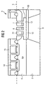
- the micromechanical sensor according to FIG. 1 is produced by first applying a sacrificial layer, which preferably consists of silicon oxide, to an SOI substrate, and then growing an epitaxial layer 4.
- the thickness of layer 4 is relatively much greater than the thickness of layer 3, so that a flat surface 5 results after this step. Possibly. it is necessary to polish this surface to improve smoothness.
- the epitaxial layer 4 grows single-crystal in the area of the wafer 2, and polycrystalline silicon is formed in the area of the material of the sacrificial layer.
- a seed layer can preferably be applied to the sacrificial layer 3, which can consist, for example, of polycrystalline silicon.
- trenches 7 are etched into the epitaxial layer 4 in the usual way, so that channels are formed which extend up to the sacrificial layer 12. These channels are then preferably filled with silicon oxide.
- an electronic semiconductor circuit using thin-film technology can be applied in a conventional manner as a further constructional feature. This can be, for example, a CMOS, Bi-CMOS or bipolar process known per se.
- the back of the substrate is then electrolessly etched, for example with KOH or TMAH, so that an opening 8 is created.
- a further etching step which can be carried out after or before the backside etching, the oxides in the channels and in the sacrificial layer are removed.
- the membrane 13 which arises during the rear side etching, is so thin that it can be excited to vibrate, for example, under the influence of a sound wave.
- the thickness of the membrane is preferably between 0.2 ⁇ m and 1 ⁇ m. It is possible to make the membrane 13 thinner in the side area of the support, so that the vibration of the membrane can take place even with smaller sound amplitudes.
- the membrane preferably has an overall length in the range from 100 ⁇ m to 2000 ⁇ m.
- the backside etching is expediently carried out without current, in particular with a KOH etching solution.
- the sacrificial layer 3 is preferably removed by Wet etching.
- the invention also relates to the use of the invention Sensors for the production of pressure sensors, in particular Relative pressure sensors, and microphones. With sensors for the Use in microphones results in advantages when the membrane is arranged in the direction of the underside of the chip area.
- an essential advantage of the arrangement according to the invention is that the membrane can consist of single-crystal material. This results in an improved mechanical resistance compared to membranes made of polycrystalline material. Compared to methods known from the prior art for Manufacture of micromechanical sensors is the inventive one Manufacturing process in a simplified manner feasible. For example, on the production of Intermediate layers, as for example in the German Patent application 196 48 424.3 are described, waived become.
- the method of the present invention also offers the advantage of a flat chip area. For example at the manufacture of circuits on the chip of the sensor after or during the manufacture of the sensor structure the process steps simplified by a flat chip area.
Landscapes
- Engineering & Computer Science (AREA)
- Manufacturing & Machinery (AREA)
- Mechanical Engineering (AREA)
- Microelectronics & Electronic Packaging (AREA)
- Physics & Mathematics (AREA)
- General Physics & Mathematics (AREA)
- Measuring Fluid Pressure (AREA)
- Pressure Sensors (AREA)
- Micromachines (AREA)
Abstract
Description
Ein weiterer Nachteil der vorstehenden Anordnung ist es, daß die Membran aus polykristallinem Silizium besteht. Polykristallines Silizium weist nicht befriedigende Eigenschaften hinsichtlich der mechanischen Festigkeit auf, was beispielsweise bei der Fertigung Probleme mit sich bringt. So muß das halbfertige Sensorelement wesentlich vorsichtiger gehandhabt werden, um Beschädigungen der empfindlichen Sensorfläche zu vermeiden. Weiterhin ergeben sich Nachteile bei der Fertigung von bekannten mikromechanischen Sensoren mit einer in Richtung der Oberseite ausgerichteter Membran. So kann es beispielsweise bei der Montage oder beim Sägen des Wafers zu Einbußen in der Produktqualität kommen.
- Figur 1
- zeigt einen mikromechanischen Sensor gemäß der Erfindung, welcher auf einem SOI-Substrat hergestellt worden ist.
- Figur 2
- zeigt einen mikromechanischen Sensor, welcher auf einem herkömmlichen Siliziumsubstrat hergestellt worden ist.
Die Rückseitenätzung wird zweckmäßigerweise stromlos, insbesondere mit einer KOH-Ätzlösung, durchgeführt.
Claims (11)
- Mikromechanischer Sensor (1) auf einem Halbleitersubstrat (2), mit auf dem Chip integriertem elektronischen Schaltkreis (11) umfassend einen Hohlraum (12), eine Membran (13), eine Gegenelektrode (14) und Ventilationsöffnungen (7), welche das Volumen des Hohlraums mit der Umgebung verbinden,
dadurch gekennzeichnet, daß
die Ventilationsöffnungen in Richtung der Oberseite des Wafers (15) auserichtet sind und die Gegenelektrode Bestandteil einer Beschichtungsebene (5) ist, die über die gesamte Chipfläche reicht, so daß auf diese Beschichtungsebene eine elektronische Halbleiter-Schaltung (11) in an sich bekannter Halbleiter-Technologie aufgebracht werden kann. - Mikromechanischer Sensor nach Anspruch 1,
dadurch gekennzeichnet, daß
die Membran aus einkristallinem Material besteht. - Sensor nach Anspruch 1,
dadurch gekennzeichnet, daß
die Gegenelektrode leitfähig ausgebildet oder mit einer leitfähigen Schicht versehen ist. - Verfahren zur Herstellung eines mikromechanischen Sensors umfassend die Schritte:a) Herstellung einer Opferschicht (3) auf einem Halbleiter-Substrat (2) in einem Bereich der Substratoberfläche,b) epitaktisches Aufwachsen lassen eines halbleitenden Materials in der Weise, daß eine ebene Schicht (5) entsteht, die den Bereich der Opferschicht überragt, wobei diese Schicht im Bereich der Opferschicht polykristallin aufwächst,c) ggf. Glätten dieser ebenen Schicht,d) Ätzen von Öffnungen (7) und Füllen der Öffnungen mit einem geeigneten Material,e) Entfernen des Materials in den Öffnungen und der Opferschicht und Rückseitenätzung des Wafers zur Freilegung der Membran und Erzeugung einer Sensor-Öffnung.
- Verfahren nach Anspruch 4,
dadurch gekennzeichnet, daß
das Substrat ein Wafer mit einer Oxid-Zwischenschicht (SOI) ist, wobei die Oxid-Zwischenschicht als Ätzstopp bei der Rückseitenätzung wirkt. - Verfahren nach einem der Ansprüche 4 oder 5,
dadurch gekennzeichnet, daß
das Stoppen der Rückseitenätzung durch geeignete Dotierung des Wafers erreicht wird. - Verfahren nach mindestens einem der Ansprüche 4 bis 6,
dadurch gekennzeichnet, daß
nach Schritt a) eine Seed-Schicht auf die Opferschicht aufgebracht wird, die beim Wachstum der ebenen Schicht, die in Schritt b) hergestellt wird, für verbesserte Wachstumsbedingungen sorgt. - Verfahren nach mindestens einem der Ansprüche 4 bis 7,
dadurch gekennzeichnet, daß
die Rückseitenätzung in Abhängigkeit von der verwendeten Schicht für den Ätzstopp entweder stromlos oder elektrochemisch naßgeätzt wird. - Verfahren nach mindestens einem der Ansprüche 4 bis 8,
dadurch gekennzeichnet, daß
die Opferschicht und das Füllmaterial, welches sich in den Öffnungen (7) befindet, Siliziumoxid ist. - Verfahren nach mindestens einem der Ansprüche 4 bis 9,
dadurch gekennzeichnet, daß
nach Schritt d) vor Schritt e) ein an sich bekanntes Verfahren zur Herstellung einer elektronischen Halbleiterschaltung durchgeführt wird. - Verwendung des mikromechanischen Sensors nach Anspruch 1 als Mikrofon oder Drucksensor.
Applications Claiming Priority (2)
| Application Number | Priority Date | Filing Date | Title |
|---|---|---|---|
| DE19836341 | 1998-08-11 | ||
| DE19836341 | 1998-08-11 |
Publications (2)
| Publication Number | Publication Date |
|---|---|
| EP0979992A1 true EP0979992A1 (de) | 2000-02-16 |
| EP0979992B1 EP0979992B1 (de) | 2003-10-08 |
Family
ID=7877180
Family Applications (1)
| Application Number | Title | Priority Date | Filing Date |
|---|---|---|---|
| EP99112978A Expired - Lifetime EP0979992B1 (de) | 1998-08-11 | 1999-07-05 | Verfahren zur Herstellung eines Mikromechanischen Sensors |
Country Status (4)
| Country | Link |
|---|---|
| US (1) | US6357299B1 (de) |
| EP (1) | EP0979992B1 (de) |
| JP (1) | JP3447625B2 (de) |
| DE (1) | DE59907268D1 (de) |
Cited By (3)
| Publication number | Priority date | Publication date | Assignee | Title |
|---|---|---|---|---|
| WO2003055271A1 (de) * | 2001-12-11 | 2003-07-03 | Infineon Technologies Ag | Mikromechanische sensoren und verfahren zur herstellung derselben |
| US6940564B2 (en) | 2001-03-23 | 2005-09-06 | Koninklijke Philips Electronics N.V. | Display substrate and display device |
| DE102007042101B4 (de) * | 2006-09-20 | 2015-11-19 | Denso Corporation | Durchflussmesselement und Massendurchflussmesser |
Families Citing this family (14)
| Publication number | Priority date | Publication date | Assignee | Title |
|---|---|---|---|---|
| JP2001326367A (ja) * | 2000-05-12 | 2001-11-22 | Denso Corp | センサおよびその製造方法 |
| JP2002131161A (ja) * | 2000-10-27 | 2002-05-09 | Denso Corp | 半導体圧力センサ |
| DE10231727A1 (de) * | 2002-07-13 | 2004-01-22 | Robert Bosch Gmbh | Mikromechanische Drucksensorvorrichtung und entsprechende Messanordnung |
| ATE466456T1 (de) * | 2003-05-26 | 2010-05-15 | Sensfab Pte Ltd | Herstellung von silicium-mikrophonen |
| JP4569322B2 (ja) * | 2005-03-02 | 2010-10-27 | 株式会社デンソー | 可動センサ素子 |
| US7449356B2 (en) * | 2005-04-25 | 2008-11-11 | Analog Devices, Inc. | Process of forming a microphone using support member |
| DE102007026445A1 (de) * | 2007-06-06 | 2008-12-11 | Robert Bosch Gmbh | Mikromechanisches Bauelement und Verfahren zur Herstellung eines mikromechanischen Bauelements |
| DE102009000416A1 (de) | 2009-01-27 | 2010-07-29 | Robert Bosch Gmbh | Mikromechanischer Drucksensor mit vertikaler Membranaufhängung |
| US8703517B2 (en) * | 2010-10-29 | 2014-04-22 | Denso Corporation | Method of Manufacturing a Semiconductor Device Including Removing a Reformed Layer |
| US20120211805A1 (en) | 2011-02-22 | 2012-08-23 | Bernhard Winkler | Cavity structures for mems devices |
| DE102012206531B4 (de) | 2012-04-17 | 2015-09-10 | Infineon Technologies Ag | Verfahren zur Erzeugung einer Kavität innerhalb eines Halbleitersubstrats |
| CN103011057A (zh) * | 2012-12-03 | 2013-04-03 | 东南大学 | 一种微电子机械系统电容式气压传感器的制备方法 |
| US9136136B2 (en) | 2013-09-19 | 2015-09-15 | Infineon Technologies Dresden Gmbh | Method and structure for creating cavities with extreme aspect ratios |
| CN106744651A (zh) * | 2017-01-11 | 2017-05-31 | 河海大学常州校区 | 一种电容式微电子气压传感器及其制备方法 |
Citations (3)
| Publication number | Priority date | Publication date | Assignee | Title |
|---|---|---|---|---|
| DE4318466A1 (de) * | 1993-06-03 | 1994-12-08 | Bosch Gmbh Robert | Mikromechanischer Sensor und Verfahren zu dessen Herstellung |
| US5677560A (en) * | 1990-05-29 | 1997-10-14 | Fraunhofer Gesellschaft Zur Forderung Der Angewandten Forschung E.V. | Micromechanical component and process for the fabrication thereof |
| DE19648424C1 (de) * | 1996-11-22 | 1998-06-25 | Siemens Ag | Mikromechanischer Sensor |
Family Cites Families (3)
| Publication number | Priority date | Publication date | Assignee | Title |
|---|---|---|---|---|
| JPS60138434A (ja) * | 1983-12-27 | 1985-07-23 | Fuji Electric Co Ltd | 半導体形静電容量式圧力センサの製造方法 |
| US5146435A (en) | 1989-12-04 | 1992-09-08 | The Charles Stark Draper Laboratory, Inc. | Acoustic transducer |
| JP3657079B2 (ja) | 1997-03-19 | 2005-06-08 | 富士通株式会社 | エンハンスメント型トランジスタ回路のバイアス回路を有する集積回路装置 |
-
1999
- 1999-07-05 DE DE59907268T patent/DE59907268D1/de not_active Expired - Lifetime
- 1999-07-05 EP EP99112978A patent/EP0979992B1/de not_active Expired - Lifetime
- 1999-08-11 US US09/372,306 patent/US6357299B1/en not_active Expired - Lifetime
- 1999-08-11 JP JP22774699A patent/JP3447625B2/ja not_active Expired - Fee Related
Patent Citations (3)
| Publication number | Priority date | Publication date | Assignee | Title |
|---|---|---|---|---|
| US5677560A (en) * | 1990-05-29 | 1997-10-14 | Fraunhofer Gesellschaft Zur Forderung Der Angewandten Forschung E.V. | Micromechanical component and process for the fabrication thereof |
| DE4318466A1 (de) * | 1993-06-03 | 1994-12-08 | Bosch Gmbh Robert | Mikromechanischer Sensor und Verfahren zu dessen Herstellung |
| DE19648424C1 (de) * | 1996-11-22 | 1998-06-25 | Siemens Ag | Mikromechanischer Sensor |
Cited By (4)
| Publication number | Priority date | Publication date | Assignee | Title |
|---|---|---|---|---|
| US6940564B2 (en) | 2001-03-23 | 2005-09-06 | Koninklijke Philips Electronics N.V. | Display substrate and display device |
| WO2003055271A1 (de) * | 2001-12-11 | 2003-07-03 | Infineon Technologies Ag | Mikromechanische sensoren und verfahren zur herstellung derselben |
| US7190038B2 (en) | 2001-12-11 | 2007-03-13 | Infineon Technologies Ag | Micromechanical sensors and methods of manufacturing same |
| DE102007042101B4 (de) * | 2006-09-20 | 2015-11-19 | Denso Corporation | Durchflussmesselement und Massendurchflussmesser |
Also Published As
| Publication number | Publication date |
|---|---|
| EP0979992B1 (de) | 2003-10-08 |
| JP2000065665A (ja) | 2000-03-03 |
| US6357299B1 (en) | 2002-03-19 |
| JP3447625B2 (ja) | 2003-09-16 |
| DE59907268D1 (de) | 2003-11-13 |
Similar Documents
| Publication | Publication Date | Title |
|---|---|---|
| EP0979992A1 (de) | Mikromechanischer Sensor | |
| DE4332843C2 (de) | Verfahren zur Herstellung einer mikromechanischen Vorrichtung und mikromechanische Vorrichtung | |
| DE19718370B4 (de) | Verfahren zum Herstellen einer Membran eines Drucksensors oder akustischen Wandlers und akustischer Wandler oder Drucksensor | |
| DE69934841T2 (de) | Druckwandler und Herstellungsverfahren | |
| DE3743080C2 (de) | Verfahren zur Herstellung eines Halbleiter-Druckfühlers | |
| DE19826317B4 (de) | Verfahren zum Herstellen eines Halbleitersubstrats, Halbleiterdrucksensor und sein Herstellungsverfahren | |
| EP0720748B1 (de) | Integrierte mikromechanische sensorvorrichtung und verfahren zu deren herstellung | |
| DE3345988A1 (de) | Halbleitervorrichtung mit einem druckfuehler sowie verfahren zu ihrer herstellung | |
| EP1105344B1 (de) | Mikromechanischer sensor und verfahren zu seiner herstellung | |
| DE4309206C1 (de) | Halbleitervorrichtung mit einem Kraft- und/oder Beschleunigungssensor | |
| DE4410631A1 (de) | Kapazitiver Sensor bzw. Wandler sowie Verfahren zu dessen Herstellung | |
| EP0367750A2 (de) | Verfahren zur Herstellung einer Siliziummenbran mit kontrollierter Spannung | |
| DE19903380B4 (de) | Halbleitersensoren für eine physikalische Grösse und ihre Herstellungsverfahren | |
| DE4318466B4 (de) | Verfahren zur Herstellung eines mikromechanischen Sensors | |
| DE4030466C2 (de) | Piezo-Widerstandsvorrichtung | |
| DE3918769C2 (de) | Halbleiterdrucksensor und Verfahren zu seiner Herstellung | |
| DE10001361A1 (de) | Verfahren zum Herstellen eines Mikroträgheitssensors | |
| DE4203833A1 (de) | Verfahren zur herstellung von siliziumhalbleiter-beschleunigungsmesser-bauelementen | |
| DE4003473C2 (de) | ||
| DE69836813T2 (de) | Verfahren zur Herstellung von Winkelgeschwindigkeitsmessern | |
| EP2125607A1 (de) | Verfahren zur herstellung eines bauteils und sensorelement | |
| DE2305902A1 (de) | Verfahren zur erzielung eines genau eingestellten hohen widerstandswerts in einem in einer einkristallinen basis gebildeten widerstand | |
| DE10161921A1 (de) | Halbleitersensor zum Erfassen einer dynamischen Grösse und Verfahren zum Herstellen desselben | |
| WO2022078771A1 (de) | Herstellungsverfahren für ein mikromechanisches bauteil für eine sensor- oder mikrofonvorrichtung | |
| DE4303423C2 (de) | Sensor und Verfahren zu dessen Herstellung |
Legal Events
| Date | Code | Title | Description |
|---|---|---|---|
| PUAI | Public reference made under article 153(3) epc to a published international application that has entered the european phase |
Free format text: ORIGINAL CODE: 0009012 |
|
| AK | Designated contracting states |
Kind code of ref document: A1 Designated state(s): DE FR GB IT NL |
|
| AX | Request for extension of the european patent |
Free format text: AL;LT;LV;MK;RO;SI |
|
| 17P | Request for examination filed |
Effective date: 20000317 |
|
| AKX | Designation fees paid |
Free format text: DE FR GB IT NL |
|
| RAP1 | Party data changed (applicant data changed or rights of an application transferred) |
Owner name: INFINEON TECHNOLOGIES AG |
|
| 17Q | First examination report despatched |
Effective date: 20020704 |
|
| GRAH | Despatch of communication of intention to grant a patent |
Free format text: ORIGINAL CODE: EPIDOS IGRA |
|
| RTI1 | Title (correction) |
Free format text: METHOD OF MANUFACTURING A MICROMECHANICAL SENSOR |
|
| GRAH | Despatch of communication of intention to grant a patent |
Free format text: ORIGINAL CODE: EPIDOS IGRA |
|
| GRAA | (expected) grant |
Free format text: ORIGINAL CODE: 0009210 |
|
| AK | Designated contracting states |
Kind code of ref document: B1 Designated state(s): DE FR GB IT NL |
|
| REG | Reference to a national code |
Ref country code: GB Ref legal event code: FG4D Free format text: NOT ENGLISH |
|
| REF | Corresponds to: |
Ref document number: 59907268 Country of ref document: DE Date of ref document: 20031113 Kind code of ref document: P |
|
| GBT | Gb: translation of ep patent filed (gb section 77(6)(a)/1977) |
Effective date: 20031223 |
|
| PG25 | Lapsed in a contracting state [announced via postgrant information from national office to epo] |
Ref country code: GB Free format text: LAPSE BECAUSE OF NON-PAYMENT OF DUE FEES Effective date: 20040705 |
|
| ET | Fr: translation filed | ||
| PLBE | No opposition filed within time limit |
Free format text: ORIGINAL CODE: 0009261 |
|
| STAA | Information on the status of an ep patent application or granted ep patent |
Free format text: STATUS: NO OPPOSITION FILED WITHIN TIME LIMIT |
|
| 26N | No opposition filed |
Effective date: 20040709 |
|
| PG25 | Lapsed in a contracting state [announced via postgrant information from national office to epo] |
Ref country code: NL Free format text: LAPSE BECAUSE OF NON-PAYMENT OF DUE FEES Effective date: 20050201 |
|
| GBPC | Gb: european patent ceased through non-payment of renewal fee |
Effective date: 20040705 |
|
| PG25 | Lapsed in a contracting state [announced via postgrant information from national office to epo] |
Ref country code: FR Free format text: LAPSE BECAUSE OF NON-PAYMENT OF DUE FEES Effective date: 20050331 |
|
| NLV4 | Nl: lapsed or anulled due to non-payment of the annual fee |
Effective date: 20050201 |
|
| REG | Reference to a national code |
Ref country code: FR Ref legal event code: ST |
|
| PG25 | Lapsed in a contracting state [announced via postgrant information from national office to epo] |
Ref country code: IT Free format text: LAPSE BECAUSE OF NON-PAYMENT OF DUE FEES Effective date: 20050705 |
|
| PGFP | Annual fee paid to national office [announced via postgrant information from national office to epo] |
Ref country code: DE Payment date: 20170912 Year of fee payment: 19 |
|
| REG | Reference to a national code |
Ref country code: DE Ref legal event code: R119 Ref document number: 59907268 Country of ref document: DE |
|
| PG25 | Lapsed in a contracting state [announced via postgrant information from national office to epo] |
Ref country code: DE Free format text: LAPSE BECAUSE OF NON-PAYMENT OF DUE FEES Effective date: 20190201 |