EP0966741B1 - Dram mit integralem sram sowie systeme und verfahren zu deren benutzung - Google Patents
Dram mit integralem sram sowie systeme und verfahren zu deren benutzung Download PDFInfo
- Publication number
- EP0966741B1 EP0966741B1 EP98911655A EP98911655A EP0966741B1 EP 0966741 B1 EP0966741 B1 EP 0966741B1 EP 98911655 A EP98911655 A EP 98911655A EP 98911655 A EP98911655 A EP 98911655A EP 0966741 B1 EP0966741 B1 EP 0966741B1
- Authority
- EP
- European Patent Office
- Prior art keywords
- address bits
- array
- accessing
- address
- bank
- Prior art date
- Legal status (The legal status is an assumption and is not a legal conclusion. Google has not performed a legal analysis and makes no representation as to the accuracy of the status listed.)
- Expired - Lifetime
Links
Images
Classifications
-
- G—PHYSICS
- G06—COMPUTING OR CALCULATING; COUNTING
- G06F—ELECTRIC DIGITAL DATA PROCESSING
- G06F12/00—Accessing, addressing or allocating within memory systems or architectures
- G06F12/02—Addressing or allocation; Relocation
- G06F12/0215—Addressing or allocation; Relocation with look ahead addressing means
-
- G—PHYSICS
- G06—COMPUTING OR CALCULATING; COUNTING
- G06F—ELECTRIC DIGITAL DATA PROCESSING
- G06F12/00—Accessing, addressing or allocating within memory systems or architectures
- G06F12/02—Addressing or allocation; Relocation
- G06F12/08—Addressing or allocation; Relocation in hierarchically structured memory systems, e.g. virtual memory systems
- G06F12/0802—Addressing of a memory level in which the access to the desired data or data block requires associative addressing means, e.g. caches
- G06F12/0893—Caches characterised by their organisation or structure
-
- G—PHYSICS
- G11—INFORMATION STORAGE
- G11C—STATIC STORES
- G11C8/00—Arrangements for selecting an address in a digital store
Definitions
- the present invention relates in general to electronic memories and in particular to a dynamic random access memory (DRAM) with integral static random access memory (SRAM. and systems and methods using the same.
- DRAM dynamic random access memory
- SRAM integral static random access memory
- DRAMs dynamic random access memories
- the typical general purpose DRAM has a single data port for writing and reading data to and from addressed storage locations ("dual ported" DRAMs are available which provide two data ports, typically one random and one serial port, however, these devices are normally limited to special memory applications).
- data writes and reads are only made on a location by location basis, with each location typically being one bit, one byte or one word wide.
- PCs personal computers
- CPU central processing unit
- All other subsystems, such as the display controller, disk drive controller, and audio controller then operate as slaves to the CPU.
- This master/slave organization is normally used no matter whether the CPU is a complex instruction set computer (CISC), reduced instruction set computer (RISC), Silicon Graphics MIPS device or Digital Equipment ALPHA device.
- CISC complex instruction set computer
- RISC reduced instruction set computer
- Silicon Graphics MIPS device Silicon Graphics MIPS device
- Digital Equipment ALPHA device Digital Equipment ALPHA
- Multiprocessing architectures are not yet cost effective for application in the PC environment.
- memory contention and bus contention are still significant concerns in any multiprocessing system, let alone in a multiprocessing PC environment.
- a dynamic random access memory having built-in cache is disclosed in United States Patent No. 5,226,139 issued to Fujishima et al., July 6, 1993 and entitled "Semiconductor Memory Device With Built-in Cache And Operating Method Thereof.”
- a memory device is partitioned into a number of banks each including a DRAM array and a SRAM cache.
- the SRAM cache is accessed, otherwise the DRAM array is accessed.
- This memory has the disadvantage of not being capable of maintaining spatial or temporal locality between banks since the latches are only updated using the last received address, such that the associated data may or may not have any locality with the data previously accessed.
- a memory which includes a plurality of banks each including first and second arrays of memory cells, first accessing circuitry for selectively accessing cells in the first array and second accessing circuitry for selectively accessing cells in the second array.
- Each bank further includes storage circuitry for storing address bits and circuitry for comparing received address bits with stored address bits in the storage circuitry.
- the first accessing circuitry accesses cells in the first array in response to the stored address bits when the stored address bits and the received address bits match.
- the second accessing circuitry accesses cells in the second array when the stored address bits and the received address bits differ.
- the global access control circuitry enables comparison of the stored address bits and the received address bits in a selected one of the plurality of banks.
- a memory subsystem including a plurality of memory banks each comprising an array of rows and columns of dynamic random access memory cells, a row decoder for selecting one of the dynamic random access memory cells for access, an array of static random access memory cells coupled to the array of dynamic random access memory cells, and a latch for storing a selected number of row address bit.
- Each bank further includes comparator circuitry for selectively comparing received row address bits and row address bits stored in the latch of the bank, the comparator circuitry initiating an access to selected cells in the static random access array when the received bits and the stored bits match and initiating an access to selected cells in the dynamic random access array when the received row address bits and the stored row address bits differ.
- the memory subsystem further includes a global row assignor for enabling the comparator circuitry of a selected one of the banks in response to selected bits of a received row address.
- an address is received having first and second sets of bits.
- a first of a plurality of banks is selected in response to the first set of bits and the second set of bits are compared with bits previously stored in first one of the banks.
- a selected one of an SRAM array and a DRAM array in the first of the banks is accessed.
- the SRAM array is accessed and if the second set of bits stored in the selected banks differ, the DRAM array is accessed.
- a first address comprising a first plurality of address bits is received.
- First data is written to a location in a first one of the banks addressed by the first plurality of bits.
- the first plurality of bits are also stored in the first bank.
- the first plurality of address bits are also modified to generate a second plurality of address bits.
- Second data is then written to a location in a second one of the banks addressed by the second plurality of address bits.
- the second plurality of address bits are stored in the second bank.
- a second address, including a third plurality of address bits, is received.
- the third plurality of address bits are compared with the first and second plurality of bits and the first bank is accessed if the first plurality of bits matches the third plurality of bits and the second bank is accessed if the second plurality of bits matches the third plurality of bits.
- the principles of the present invention allow for the construction of high speed memory devices.
- the use of SRAM allows data to be clocked out rapidly and with additional drive.
- FIGURES 1-5 of the drawings in which like numbers designate like parts.
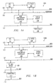
- FIGURES 1A and 1B are block diagrams respectively depicting two basic system architectures 100A and 100B typical of those found in personal computers (PCs). While numerous variations on these basic architectures exist, FIGURES 1A and 1B are suitable for describing the basic structure and operation of most PCs.
- Both systems 100A and 100B include a single central processing unit 101, CPU local data bus 102. CPU local address bus 103. external (L2) cache 104, core logic/memory controller 105, and system memory 106.
- the peripherals 108 are coupled directly to core logic/memory controller 105 via a bus 107.
- Bus 107 in this case is preferably a peripheral controller interface (PCI) bus, although alternatively it could be an ISA, general. or special purpose bus, as known in the art.
- PCI peripheral controller interface
- core logic/memory controller 105 is again coupled to bus 107.
- a PCI bus bridge then interfaces bus 107 with a PCI bus 110, to which the peripherals 111 couple.
- An additional bus 112 which may be a ISA, PCI, VESA, IDE, general, or special purpose bus, is provided for access to peripherals 111 from an external device or system (not shown).
- CPU 101 In single CPU systems 100A and 100B, CPU 101 is the "master" which, in combination with the operating system and applications software, controls the overall operation of system 100. Among other things, CPU 101 performs various data processing functions including numerical and word processing, generates graphics data, and performs overall system management.
- CPU 101 may be for example a complex instruction set computer (CISC), such as an Intel Pentium class microprocessor, a reduced instruction set computer (RISC), such as a Apple PowerPC microprocessor, or a very long instruction word (VLIW) machine.
- CISC complex instruction set computer
- RISC reduced instruction set computer
- VLIW very long instruction word
- CPU 101 communicates with the remainder of system 100 via CPU local address and data buses 102 and 103. each of which may be for example a special bus, or a general bus. as known in the art.
- Core logic/memory controller 105 under the direction of CPU 101, controls the exchange of data, addresses, control signals and instructions between CPU 101, system memory 105, and peripherals 108/111 via bus 107 and/or PCI bus bridge 109. Although the core logic/memory controller allows tasks to be shifted from the CPU, thereby allowing the CPU to attend to other CPU-intensive tasks, the CPU can always override core logic/memory controller 105 to initiate execution of a higher priority task.
- the memory controller can be either a separate device or incorporated into the same chip set as the core logic.
- the memory controller is generally responsible for generating the memory clocks and control signals such as /RAS, /CAS, R/W and bank select, and monitors and controls cell refresh.
- the memory controller may also have some address generation capability for accessing sequences of pages.
- the core logic is typically comprised of a chip-set, with one or more chips typically being “address and system controller intensive” and one or more chips typically being “data intensive.”
- the address intensive chip(s) interfaces CPU 101 with address bus 103; maintains cache memory, including the cache tags, set associative cache tags and other data necessary to insure cache coherency; performs cache "bus snooping"; generates the control signals required for DRAMs in the system memory or cache; and controls general management transactions.
- the data intensive chip(s) generally: interfaces CPU 101 with the data bus 102; issues cycle completion responses; may abort operations if their cycles are incomplete; and arbitrates for the data path of bus 102.
- L2 cache 104 may be for example a 256 KByte fast SRAM device(s).
- the CPU also maintains up to 16 kilobytes of on-chip (L1) cache.
- PCI bus bridges such as PCI bus bridge 109, are also well known to those skilled in the art.
- the CPU is the bus master for the entire system and hence devices such as PCI bus bridge are slave devices which operate under command of the CPU.
- Peripherals 107/111 may include a display controller and associated frame buffer, floppy drive controller, disk driver controller, and/or modem, to name only a few options.
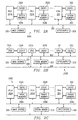
- FIGURES 2A, 2B and 2C respectively depict exemplary multiprocessor architectures 200A, 200B and 200C for discussion purposes.
- Multiprocessing system 200A is based upon n number of CPUs 201.
- Each CPU 201 is associated with a dedicated cache 202 and dedicated (private) system memory 203.
- Common bus 204 allows a given CPU to exchange information with peripherals, including mass storage subsystems 204, such as disk drives, tape drives and cartridge units, and Input/Output subsystems 206, such as printers, displays and keyboards.
- NORMA no read/write memory access
- System 200B also primarily includes n number of CPUs 201, each with an associated cache 202. and coupled to the peripheral devices through a common bus 204.
- system memory 207 is also coupled to bus 204 and is shared by all the CPUs 201.
- a second bus 206 is provided as a second path for accessing system memory 207.
- the memory architecture of system 200B is typically designated as a unified memory access (UMA) architecture. Under the UMA paradigm, all processors have equal access to system memory and all processors have local cache.
- UMA unified memory access
- the unified memory access architecture typically provides the fastest possible interaction between processors and is the common architecture used in PCs, work stations, and other desktop computing devices. UMA based systems are often referred to as "symmetric- multiprocessing" systems.
- System 200C is a system in which both private and system memory are provided. Specifically, in addition to dedicated cache 202, each CPU 201 is also associated with private memory 209. Each CPU is further connected by bus 204 to a shared system memory 210.
- the memory architecture of system 200C falls under the non-uniform memory access (NUMA) paradigm.
- NUMA non-uniform memory access
- each processor has a private memory and additionally shares system memory with the other processors in the system.
- One difficulty in a NUMA based system is the fact that the access times for the private and system memories may be different creating timing problems.
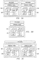
- FIGURES 2A, 2B and 2C there are a number of ways to implement the hardware architectures shown in FIGURES 2A, 2B and 2C in a complete hardware/software system. Three such systems arc shown in FIGURES 3A-3C, respectively.
- FIGURE 3A is a diagram illustrating a "loosely coupled" multiprocessing architecture.
- each processing node 300 maintains a dedicated copy of both the operating system and the application programs.
- Loosely coupled architectures such as that shown in FIGURE 3A. are used often in embedded systems and in real-time systems in which tasks must be partitioned to different processing nodes for synchronization purposes.
- Embedded systems include those in which the CPU is fabricated on the same chip as logic, memory, a signal processor, or the like.
- High speed interconnects are used to share data and pass messages between processing nodes 300. While loosely coupled systems are more fault and error tolerant, their software programming is most often highly complex.
- FIGURE 3B depicts a "tightly coupled" system.
- a single copy of the operating system and a single copy of the application program are shared and executed by a single set of processors.
- writing software programs for a tightly coupled system is normally simpler than for writing programs to a loosely coupled system.
- tightly coupled systems based only on single copies of the application programs and operating system, are less tolerant to errors and failures than the loosely coupled systems.
- FIGURE 3C is a diagram of a "snugly coupled" system in which each processing node 300 maintains a dedicated copy of the operating system and all nodes share a single copy of the applications program.
- the snugly coupled variation is a hybrid which provides the tolerance to failure/ errors found in loosely coupled systems while still providing the simpler program found in tightly coupled systems.
- CISC CPU may be "latency” dominated while a digital signal processor (DSP) based system may be "dataflow” dominated.
- DSP digital signal processor
- pipelined processing algorithms typically are dataflow intensive. since the processors perform operations on streams of data received from other processors in the system and then pass the results on to other processors.
- contention problems can be solved by "memory locking."
- memory locking is a memory management task which may be performed by the memory management unit (MMU) on-board the CPUs themselves or by a stand-alone device or subsystem. In any event. memory locking reduces the efficiency which multiprocessing was intended to increase, since during a contention situation, at least one processor must wait to access data.
- MMU memory management unit
- Symmetric multiprocessing operating systems are preferred, since this type of operating system is capable of seamlessly passing application programs to the CPUs as they become available.
- the selection of between tightly, loosely and snugly coupled software architecture requires substantial trade-offs, and in particular trade offs between ease of programming and fault/error tolerance.
- bus contention problems may also arise. Specifically, when a shared bus is employed, only one processor is normally granted access to the bus to perform a given bus task, while the remainder of the processors coupled to that bus must wait until their priority has been reached.
- One technique for minimizing bus contention problems is to provide a dedicated cache for each CPU, as shown in FIGURES 3A-3C, so that a given CPU need only access the bus at times when required data are not found in the dedicated cache.
- cache coherency is a major concern in the design of a multiprocessing system. In other words, when a given processor modifies a location in memory, some technique must be provided for insuring that the data is modified in the cache memory of each of the other processors using the same data.
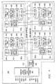
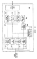
- FIGURE 4 is a functional block diagram of a dynamic random access memory device 400 according to one embodiment of the principles of the present invention.
- Memory 400 includes N number of memory banks or units 401, with four such banks 401a, 401b, 401c, and 401d being shown in FIGURE 4 for discussion; the actual number of banks will vary from application to application, although N is preferably an even number two or greater.
- Banks 401 communicate with external circuitry through control and configuration circuitry 407, discussed further below.
- memory subsystem 400 may be used to construct system memory 106, although many other applications in the single CPU personal computer environment are possible, such as in the display frame buffer, in multiprocessing architectures, such as systems 200a, 200b, and 200c, memory subsystem 400 can be used to construct either the system memories or the local (private) memories.
- subsystem 400 is a monolithic integrated circuit device.
- Each bank 401 includes an array 402 of dynamic random access memory (DRAM) cells arranged in N number rows and M number columns. As is known to those skilled in the art, each array 402 may be partitioned into multiple subarrays, with the columns organized using either an open-bitline or folded-bitline approach.
- Each bank 401 further includes a traditional DRAM row decoder 404 coupled to the array wordlines, and traditional DRAM sense amplifiers/ column decoder circuitry 405 coupled to the array bitlines.
- the row and column decoders are preferably organized in hierarchical fashion in which a main decoder and one or more levels of subdecoders/drivers are used.
- each row decoder 404 in response to a row address, selects one of N rows for access during an active cycle when the row address strobe /RAS is in a logic low state.
- Column decoder selects P number of pages (locations) of C number of columns (bits) from the M total number of columns in response to P number of column addresses for access during an active cycle.
- Global row assignor 406 performs a "coarse granularity decoding" using L number of least significant row address bits from each received row address. Specifically, all banks 401 are active during each /RAS cycle, and global row assignor using the L least significant row address bits to select. Row decoders 404 consequently decode the Y-1 number of remaining most significant address bits to simultaneously select one row per /RAS cycle in each DRAM array during a DRAM access.
- Control circuitry 407 receives conventional DRAM control signals and clocks from an external source, such as processor 101 or core logic 105 in system 100 or CPUs 201 in multiprocessing systems 200A-200C. These signals include a synchronous clock (SCLK). a row address strobe (/RAS), a column address strobe (/CAS), read/write select (R/W) and output enable (/OE). along with data (DQ) and addresses (Add). Control circuitry 407 also inputs a configuration bit (CONFIG). discussed below. In the preferred embodiment, the address input port is multiplexed in a conventional manner wherein row addresses and column addresses are received sequentially at the same pins and latched in with /RAS and /CAS respectively.
- a configuration bit CONFIG
- each bank 401 further includes static random access memory (SRAM)/SRAM column decoder circuitry 408.
- SRAM circuitry 408 will be discussed in further detail in conjunction with FIGURE 5 but can generally be described at this point as follows. First, a linear array of M number of SRAM cells is included for storing a row of data transferred from the corresponding DRAM array 402. Second, SRAM column decoder circuitry is included for page access (reads or writes) of C-bit wide pages of data to the row of data in SRAM array in response to one or more column addresses.
- Data latches 409 interface the DRAM sense amplifiers/ column decoders 405 and the SRAM column decoders 408 with a data bus 410.
- Column addresses are transferred via a column address bus 411 and row addresses by a row address bus 412.
- Address latches and last row read (LRR) compare circuitry 413 includes latches for storing the current row and column addresses received at the address port A dd 0-A dd Y. Also included as part of circuitry 413 are latches for storing the high order (MSB) row address bits of the last row read (LRR) and comparison circuitry for comparing the stored LRR bits to the high order bits (MSB) of the current row address.
- MSB high order row address bits of the last row read
- MSB high order bits
- the least significant row address bits are processed by global assignor 406 and the most significant row address bits are used internal to the banks 401 to select individual rows of cells, other arrangements will just as easily apply. For example, a given number of most significant row address bits could be used by global row assignor 406 and the remaining least significant bits used for individual row select. Further, either big- or little-endian data structures can be used.
- the number of address bits presented to the SRAM cache of a given bank 408 is identical to the number of MSB address bits presented to DRAM row decoder 404.
- FIGURE 5 is a more detailed diagram emphasizing the data and address routing circuitry of a selected bank 401. Addresses are received in a multiplexed fashion at the address port Add0 - AddY. The row address bits are latched on the falling edge of /RAS (which follows the SCLK) into row address latch 501. The most significant bits are presented to the fine granularity row decoders 404 and the least significant bits to the global row assignor 406. The most significant row address bits from the previous (last) /RAS cycle are transferred to last row read address latch 502. Comparison circuitry 503 compares the most significant row address bits latched into row address latch 501 and the last read row address held in latch 502. During each /CAS cycle, one or more column addresses are received at address port Add0 - AddY and latched into column address latch 504 with each falling edge of /CAS.
- /RAS which follows the SCLK
- SRAM registers 506 store data associated with the address bits stored last read address latch 502 (i.e., assuming that row addresses and data are considered together as a data structure, the row address MSBs comprise the row field and the data bits. the data field).
- a second column decoder 507 is provided to access locations in SRAM registers 506.
- a row address is first received at address pins Add0 - AddY.
- the least significant row address bits (in the four bank embodiment, the two least significant bits) are passed to global row assignor 406 and the remaining most significant bits are latched into row address latch 501 of each bank 401.
- the most significant bits stored in each row address latch 501 from the previous /RAS cycle are transferred into the corresponding LRR address latch 502.
- the bit CONFIG at the input to memory 400 is set to a logic low.
- Global row assignor 406 determines from the current least significant row address bits the bank 401 which corresponds to the address space of the received address.
- the comparator 503 of the corresponding bank 401 is enabled such that during the period between the falling edge of /RAS and the first high to low transition of /CAS, that comparator 503 compares the current address most significant bits in the corresponding row address latch 501 and bits stored in LRR address latch 502. If a match occurs for the given bank, the SRAM column address decoders 507 are selected and set-up to access the complete SRAM cell array 506 of that bank.
- each SRAM column decoder 507 accordingly allows access to a C-bit word per each of P number of column addresses latched-in with /CAS.
- the accesses are implemented through a C-bit wide data bus 410: if for example, each bank is organized as a by 16 device, data bus 410 is 16-bits wide and so on.
- the selected (enabled) bank is the only bank 401 accessed via data bus 410, the word of data in the data latches 409 of the other banks is simply not used.
- the address bits in latches 501 and 502 do not match for the bank 401 addressed by the received row address LSBs, access must be made to the corresponding DRAM array. Specifically, for a read to the addressed bank 401. the row is selected by DRAM row decoder 404 from the corresponding DRAM array 402 and an entire row of data transferred to the associated SRAM array 506 for output when the column addresses are presented. For the remaining banks 401, the MSBs are incremented or decremented using the corresponding row address increment circuitry 508. A row of data for these banks is similarly transferred to the corresponding SRAM arrays 507.
- the received row address has LSBs 01 indicating the address space of bank 401b (Bank 1) is to be accessed.
- Global row assignor 406 hence enables Bank1 to make the comparison of the row current address MSBs and the bits stored in the Bank1 LRR latch.
- the row address MSBs as received are not modified for transferring data from the bank 401b DRAM array 402 to the Bank1 SRAM array.
- bank 401a (Bank0) the row address MSBs are decremented by 01 by the corresponding row increment circuitry 508 and the row address MSBs for banks 401c (Bank2) and 401d (Bank3) are incremented by 01 and 10 respectively.
- address A+1 the address to Bank1 (the received row address MSBs) is designated address A+1
- address A+1 is decremented by one such that Bank0 receives address AO and incremented such that Bank2 receives address A+2 and Bank3 receives address A+3.
- These addresses are used to access the associated bank's DRAM array 402 and the accessed data in DRAM transferred to the SRAM arrays.
- the new addresses are stored in address latches 501.
- the DRAM of any bank including in this case the DRAM array 402 of Bank1 can be refreshed.
- the DRAM column decoders 405 isolate the corresponding DRAM arrays 402 from the SRAM arrays 408.
- Refresh is preferably performed by incrementing the row addresses in each bank using increment and refresh circuitry 508 and latching each row of data using the DRAM sense amplifiers 405 in a conventional fashion.
- the /RAS cycle is complete.
- the data in the SRAM arrays 506 of the remaining banks 401 is available through the associated data latches 409, and could be used. but typically is reserved for future /RAS cycles.
- the current row address MSBs for the selected banks and the new row address MSBs are transferred to the LRR registers during the next /RAS cycle.
- the corresponding data remain in the SRAM arrays.
- the CPU and/or operating system typically accesses data within temporally or spacially adjacent areas in memory, the probability is substantial that a match will occur.
- An address is received at address port Add0-AddY.
- global row assignor 406 determines the bank 401 assigned to the corresponding row address space. Assume again for example, the LSBs are 01, addressing bank 401b (Bank 1 ). The received row MSBs are taken as the address to the Bank1 DRAM array 402. As was done above, the row address increment circuitry 508 for Bank0 decrements the received row MSBs to obtain a row address to the Bank0 DRAM array and increments the received MSBs by 01 and 10 to obtain row addresses to the DRAM arrays of Bank2 and Bank3 respectively. The MSB row address bits for each bank 401 is written into the bank's LRR register 502.
- the CONFIG bit at the input to memory 400 is set high.
- the MSBs of a received address are compared by all the comparators 503. If a match occurs in any one or more banks 401, the data from all the banks is taken, although the data from the non-matching banks may be discarded or left in the data latches.
Landscapes
- Engineering & Computer Science (AREA)
- Theoretical Computer Science (AREA)
- Physics & Mathematics (AREA)
- General Engineering & Computer Science (AREA)
- General Physics & Mathematics (AREA)
- Microelectronics & Electronic Packaging (AREA)
- Dram (AREA)
- Memory System Of A Hierarchy Structure (AREA)
- Apparatus For Radiation Diagnosis (AREA)
- Control Of Electric Motors In General (AREA)
- Detergent Compositions (AREA)
Claims (12)
- Speicher (400) mit einer Vielzahl von Bänken (401), jede mit einem ersten und einem zweiten Array aus Speicherzellen (402, 506), einer ersten Zugriffsschaltung (507), um wahlweise auf Zellen in dem ersten Array (506) zuzugreifen, einer zweiten Zugriffsschaltung (405), um wahlweise auf Zellen in dem zweiten Array (402) zuzugreifen, einer Speicherschaltung (502) zum Speichern von Ädressbits, die mit Daten in Beziehung stehen, auf die über das erste Array (506) zugegriffen werden kann, und einer Schaltung (508) zum Vergleichen empfangener Adressbits mit in der Speicherschaltung (502) gespeicherten Adressbits, wobei die erste Zugriffsschaltung (507) auf Zellen in dem ersten Array (506) zugreift, die durch die gespeicherten Adressbits adressiert sind, wenn die gespeicherten Adressbits und die empfangenen Adressbits übereinstimmen, und wobei die zweite Zugriffsschaltung (402) auf Zellen in dem zweiten Array (402) zugreift, die durch die empfangenen Adressbits adressiert sind, wenn die gespeicherten Adressbits und die empfangenen Adressbits verschieden sind, und einer globalen Zugriffssteuerschaltung (406), die steuerbar ist, um einen Vergleich der gespeicherten Adressbits und der empfangenen Adressbits in einer ausgewählten Bank der Vielzahl von Bänken (401) durchzuführen, wobei der Speicher gekennzeichnet ist durch:eine Schaltung (508), um wahlweise die empfangenen Bits zu verarbeiten, um zweite Bits zu erzeugen, die von den empfangenen Bits verschieden sind, um Inhalte der Speicherschaltung (502) und des ersten Arrays (506) aus Speicherzellen von einer zweiten ausgewählten Bank der Bänke (401) zu aktualisieren, wobei durch die zweiten Adressbits auf Zellen in dem zweiten Array (402) der zweiten Bank (401) zugegriffen wird, die eine vorbestimmte Position bezüglich der Zellen in dem zweiten Array (402) der ersten Bank (401) haben, auf die durch die empfangenen Adressbits zugegriffen wird.
- Speicher nach Anspruch 1, bei dem das erste Array (506) ein Array aus statischen Speicherzellen mit wahlfreiem Zugriff enthält.
- Speicher nach Anspruch 1, bei dem das zweite Array (402) ein Array aus dynamischen Speicherzellen mit wahlfreiem Zugriff enthält.
- Speicher nach Anspruch 1, bei dem die erste Zugriffsschaltung (507) einen Spalten-Dekoder zum Auswählen einer Position entlang einer Zeile in dem ersten Array enthält.
- Speicher nach Anspruch 1, bei dem die zweite Zugriffsschaltung (404, 405) einen Zeilen-Dekoder zum Auswählen einer Zeile in dem zweiten Array und einen Spalten-Dekoder zum Zugreifen auf Zellen entlang der ausgewählten Zeile enthält.
- Speicher nach Anspruch 1, bei dem die erste und die zweite Zugriffsschaltung (404, 405, 507) steuerbar ist, um einen ausgewählten Satz von Daten aus dem zweiten Array zu dem ersten Array zu übertragen.
- Speicher nach Anspruch 1, außerdem mit einem Datenspeicher (409), der mit der ersten und der zweiten Zugriffsschaltung gekoppelt ist.
- Verfahren zum Zugreifen auf Daten in einem Speichersystem (400) mit einer Vielzahl von Bänken (401), mit Empfangen einer Adresse mit einem ersten und zweiten Satz von Adressbits, Auswählen einer Bank aus einer Vielzahl von Bänken (401) in Reaktion auf den ersten Satz von Adressbits, Vergleichen des ersten Satzes von Adressbits mit Adressbits, die in der ausgewählten Bank der Bänke (401) gespeichert sind, und, wenn der zweite Satz von Adressbits mit den in der Bank gespeicherten Adressbits übereinstimmt, Zugreifen auf ein SRAM-Array (506) in der ausgewählten Bank, und, wenn der zweite Satz von Adressbits und die in der ausgewählten Bank gespeicherten Adressbits unterschiedlich sind, Zugreifen auf ein DRAM-Array (402) in der ausgewählten Bank, wobei das Verfahren außerdem die Schritte umfasst:Aktualisieren von Daten, die in einem SRAM-Array (506) der zweiten Bank (401) gespeichert sind, gekennzeichnet durch die Unterschritte:Verarbeiten des zweiten Satzes von Adressbits, um einen dritten Satz von Adressbits zu erzeugen, der von dem zweiten Satz von Bits verschieden ist, und Adressieren von Daten in einem DRAM-Array (402) der zweiten Bank (401), wobei die adressierten Daten eine vorbestimmte Position bezüglich der Daten haben, auf die über das DRAM-Array (402) der ersten Bank zugegriffen wird;Übertragen der adressierten Daten von dem DRAM-Array (402) in der zweiten Bank zu einem SRAM-Array (506) in der zweiten Bank (401); undSpeichern des dritten Satzes von Adressbits in der zweiten Bank (401); Empfangen der zweiten Adresse, wobei die zweite Adresse einen ersten und zweiten Satz von Bits enthält;Vergleichen des zweiten Satzes von Adressbits der zweiten Adresse mit dem dritten Satz von Adressbits, der in der zweiten Bank der Bänke (401) gespeichert ist; undin Reaktion auf den Schritt des Vergleichens, Zugreifen auf ein ausgewähltes Array von einem SRAM-Array (506) und einem DRAM-Array (402) in der zweiten Bank der Bänke, mit den Unterschritten:wenn der zweite Satz von Adressbits der zweiten Adresse mit dem dritten Satz von Adressbits übereinstimmt, der in der zweiten Bank (401) gespeichert ist, Zugreifen auf das SRAM-Array (506) der zweiten Bank (401); undwenn der zweite Satz von Adressbits der zweiten Adresse und der dritte Satz von Adressbits, der in der zweiten Bank gespeichert ist, unterschiedlich sind, Zugreifen auf das DRAM-Array (402) der zweiten Bank (401).
- Verfahren nach Anspruch 8, bei dem der Unterschritt des Zugreifens auf das DRAM-Array (402) den Unterschritt des Übertragens ausgewählter Daten von dem DRAM-Array (402) zu dem SRAM-Array (506) der ausgewählten Bank (401) umfasst.
- Verfahren nach Anspruch 8, bei dem der erste Satz von Adressbits niedrigstwertige Zeilen-Adressbits und der zweite Satz von Bits höchstwertige Zeilen-Adressbits enthält.
- Verfahren nach Anspruch 8, bei dem der Unterschritt des Zugreifens auf das SRAM den Unterschritt des Empfangens einer Sequenz von Spalten-Adressen und, in Reaktion, des Zugreifens auf eine Vielzahl von Speicherpositionen in dem SRAM-Array (506) umfasst.
- Verfahren nach Anspruch 11, bei dem der Schritt des Modifizierens des zweiten Satzes von Adressbits den Schritt des Modifizierens des zweiten Satzes von Adressbits umfasst, um einen dritten Satz von Adressbits zu erzeugen, der einen Satz von. Daten in dem DRAM (402) der zweiten Bank (401) in einem Adressraum adressiert, der zu dem Adressraum benachbart ist, der durch den zweiten Satz von Adressbits adressiert ist.
Applications Claiming Priority (3)
| Application Number | Priority Date | Filing Date | Title |
|---|---|---|---|
| US08/816,663 US5835932A (en) | 1997-03-13 | 1997-03-13 | Methods and systems for maintaining data locality in a multiple memory bank system having DRAM with integral SRAM |
| US816663 | 1997-03-13 | ||
| PCT/US1998/005048 WO1998040891A1 (en) | 1997-03-13 | 1998-03-13 | Dram with integral sram and systems and methods using the same |
Publications (2)
| Publication Number | Publication Date |
|---|---|
| EP0966741A1 EP0966741A1 (de) | 1999-12-29 |
| EP0966741B1 true EP0966741B1 (de) | 2003-06-04 |
Family
ID=25221300
Family Applications (1)
| Application Number | Title | Priority Date | Filing Date |
|---|---|---|---|
| EP98911655A Expired - Lifetime EP0966741B1 (de) | 1997-03-13 | 1998-03-13 | Dram mit integralem sram sowie systeme und verfahren zu deren benutzung |
Country Status (8)
| Country | Link |
|---|---|
| US (2) | US5835932A (de) |
| EP (1) | EP0966741B1 (de) |
| JP (1) | JP2001525086A (de) |
| KR (1) | KR20000076226A (de) |
| AT (1) | ATE242536T1 (de) |
| DE (1) | DE69815308D1 (de) |
| TW (1) | TW389903B (de) |
| WO (1) | WO1998040891A1 (de) |
Families Citing this family (41)
| Publication number | Priority date | Publication date | Assignee | Title |
|---|---|---|---|---|
| US6388314B1 (en) | 1995-08-17 | 2002-05-14 | Micron Technology, Inc. | Single deposition layer metal dynamic random access memory |
| US5838631A (en) | 1996-04-19 | 1998-11-17 | Integrated Device Technology, Inc. | Fully synchronous pipelined ram |
| US5835932A (en) * | 1997-03-13 | 1998-11-10 | Silicon Aquarius, Inc. | Methods and systems for maintaining data locality in a multiple memory bank system having DRAM with integral SRAM |
| US5903491A (en) | 1997-06-09 | 1999-05-11 | Micron Technology, Inc. | Single deposition layer metal dynamic random access memory |
| AU9798798A (en) * | 1997-10-10 | 1999-05-03 | Rambus Incorporated | Power control system for synchronous memory device |
| US6173356B1 (en) * | 1998-02-20 | 2001-01-09 | Silicon Aquarius, Inc. | Multi-port DRAM with integrated SRAM and systems and methods using the same |
| US6115320A (en) | 1998-02-23 | 2000-09-05 | Integrated Device Technology, Inc. | Separate byte control on fully synchronous pipelined SRAM |
| US6272594B1 (en) * | 1998-07-31 | 2001-08-07 | Hewlett-Packard Company | Method and apparatus for determining interleaving schemes in a computer system that supports multiple interleaving schemes |
| US6237130B1 (en) * | 1998-10-29 | 2001-05-22 | Nexabit Networks, Inc. | Chip layout for implementing arbitrated high speed switching access of pluralities of I/O data ports to internally cached DRAM banks and the like |
| US6467018B1 (en) * | 1999-01-04 | 2002-10-15 | International Business Machines Corporation | Method and apparatus for addressing individual banks of DRAMs on a memory card |
| JP2000268559A (ja) * | 1999-03-12 | 2000-09-29 | Nec Corp | 半導体集積回路装置 |
| JP2000339954A (ja) | 1999-05-31 | 2000-12-08 | Fujitsu Ltd | 半導体記憶装置 |
| US7069406B2 (en) * | 1999-07-02 | 2006-06-27 | Integrated Device Technology, Inc. | Double data rate synchronous SRAM with 100% bus utilization |
| US6272070B1 (en) | 2000-02-09 | 2001-08-07 | Micron Technology, Inc. | Method and apparatus for setting write latency |
| JP2001243211A (ja) * | 2000-02-29 | 2001-09-07 | Mitsubishi Electric Corp | マイクロコンピュータ |
| US6766431B1 (en) * | 2000-06-16 | 2004-07-20 | Freescale Semiconductor, Inc. | Data processing system and method for a sector cache |
| US6658523B2 (en) * | 2001-03-13 | 2003-12-02 | Micron Technology, Inc. | System latency levelization for read data |
| US7085186B2 (en) | 2001-04-05 | 2006-08-01 | Purple Mountain Server Llc | Method for hiding a refresh in a pseudo-static memory |
| JP4731730B2 (ja) * | 2001-06-04 | 2011-07-27 | ルネサスエレクトロニクス株式会社 | 半導体記憶装置 |
| JP3851865B2 (ja) * | 2001-12-19 | 2006-11-29 | 株式会社東芝 | 半導体集積回路 |
| US6728159B2 (en) * | 2001-12-21 | 2004-04-27 | International Business Machines Corporation | Flexible multibanking interface for embedded memory applications |
| US6751113B2 (en) * | 2002-03-07 | 2004-06-15 | Netlist, Inc. | Arrangement of integrated circuits in a memory module |
| US7254690B2 (en) * | 2003-06-02 | 2007-08-07 | S. Aqua Semiconductor Llc | Pipelined semiconductor memories and systems |
| US7139213B2 (en) | 2003-06-02 | 2006-11-21 | Silicon Aquarius, Inc. | Multiple data path memories and systems |
| US7707330B2 (en) * | 2003-09-18 | 2010-04-27 | Rao G R Mohan | Memories for electronic systems |
| US20050018495A1 (en) * | 2004-01-29 | 2005-01-27 | Netlist, Inc. | Arrangement of integrated circuits in a memory module |
| KR100632946B1 (ko) * | 2004-07-13 | 2006-10-12 | 삼성전자주식회사 | 불 휘발성 메모리 장치 및 그것의 프로그램 방법 |
| US7755961B2 (en) * | 2006-07-07 | 2010-07-13 | Rao G R Mohan | Memories with selective precharge |
| US7724593B2 (en) * | 2006-07-07 | 2010-05-25 | Rao G R Mohan | Memories with front end precharge |
| US7995409B2 (en) * | 2007-10-16 | 2011-08-09 | S. Aqua Semiconductor, Llc | Memory with independent access and precharge |
| US8095853B2 (en) | 2007-10-19 | 2012-01-10 | S. Aqua Semiconductor Llc | Digital memory with fine grain write operation |
| US20090182977A1 (en) * | 2008-01-16 | 2009-07-16 | S. Aqua Semiconductor Llc | Cascaded memory arrangement |
| US8521951B2 (en) * | 2008-01-16 | 2013-08-27 | S. Aqua Semiconductor Llc | Content addressable memory augmented memory |
| US8050080B2 (en) * | 2008-03-05 | 2011-11-01 | S. Aqua Semiconductor Llc | Random access memory with CMOS-compatible nonvolatile storage element in series with storage capacitor |
| US8000140B2 (en) * | 2008-03-24 | 2011-08-16 | S. Aqua Semiconductor, Llc | Random access memory with CMOS-compatible nonvolatile storage element |
| US7885110B2 (en) * | 2008-03-25 | 2011-02-08 | Rao G R Mohan | Random access memory with CMOS-compatible nonvolatile storage element and parallel storage capacitor |
| US7916572B1 (en) | 2008-07-28 | 2011-03-29 | Altera Corporation | Memory with addressable subword support |
| JP5165630B2 (ja) * | 2009-04-09 | 2013-03-21 | 京セラコネクタプロダクツ株式会社 | コネクタ |
| US9384824B2 (en) * | 2012-07-10 | 2016-07-05 | Hewlett Packard Enterprise Development Lp | List sort static random access memory |
| US10020036B2 (en) * | 2012-12-12 | 2018-07-10 | Nvidia Corporation | Address bit remapping scheme to reduce access granularity of DRAM accesses |
| US9824024B1 (en) * | 2014-10-31 | 2017-11-21 | Altera Corporation | Configurable storage blocks with embedded first-in first-out and delay line circuitry |
Family Cites Families (19)
| Publication number | Priority date | Publication date | Assignee | Title |
|---|---|---|---|---|
| JPS5943786B2 (ja) * | 1979-03-30 | 1984-10-24 | パナフアコム株式会社 | 記憶装置のアクセス方式 |
| US4292674A (en) * | 1979-07-27 | 1981-09-29 | Sperry Corporation | One word buffer memory system |
| US4758993A (en) * | 1984-11-19 | 1988-07-19 | Fujitsu Limited | Random access memory device formed on a semiconductor substrate having an array of memory cells divided into sub-arrays |
| US4894770A (en) * | 1987-06-01 | 1990-01-16 | Massachusetts Institute Of Technology | Set associative memory |
| US5226147A (en) * | 1987-11-06 | 1993-07-06 | Mitsubishi Denki Kabushiki Kaisha | Semiconductor memory device for simple cache system |
| US4897770A (en) | 1988-03-04 | 1990-01-30 | Dennis Solomon | Symmetrical color changer system |
| JP2777247B2 (ja) * | 1990-01-16 | 1998-07-16 | 三菱電機株式会社 | 半導体記憶装置およびキャッシュシステム |
| JP2938511B2 (ja) * | 1990-03-30 | 1999-08-23 | 三菱電機株式会社 | 半導体記憶装置 |
| JP2862948B2 (ja) * | 1990-04-13 | 1999-03-03 | 三菱電機株式会社 | 半導体記憶装置 |
| US5269010A (en) * | 1990-08-31 | 1993-12-07 | Advanced Micro Devices, Inc. | Memory control for use in a memory system incorporating a plurality of memory banks |
| EP0492776B1 (de) * | 1990-12-25 | 1998-05-13 | Mitsubishi Denki Kabushiki Kaisha | Halbleiterspeichervorrichtung mit einem grossen Speicher und einem Hochgeschwindigkeitsspeicher |
| JPH04307495A (ja) * | 1991-04-04 | 1992-10-29 | Mitsubishi Electric Corp | 半導体記憶装置 |
| US5680570A (en) * | 1991-06-12 | 1997-10-21 | Quantum Corporation | Memory system with dynamically allocatable non-volatile storage capability |
| EP0552667B1 (de) * | 1992-01-22 | 1999-04-21 | Enhanced Memory Systems, Inc. | DRAM mit integrierten Registern |
| JP3304413B2 (ja) * | 1992-09-17 | 2002-07-22 | 三菱電機株式会社 | 半導体記憶装置 |
| JP3305056B2 (ja) * | 1993-08-31 | 2002-07-22 | 沖電気工業株式会社 | ダイナミックram |
| US5761694A (en) * | 1995-11-30 | 1998-06-02 | Cirrus Logic, Inc. | Multi-bank memory system and method having addresses switched between the row and column decoders in different banks |
| US5787457A (en) * | 1996-10-18 | 1998-07-28 | International Business Machines Corporation | Cached synchronous DRAM architecture allowing concurrent DRAM operations |
| US5835932A (en) * | 1997-03-13 | 1998-11-10 | Silicon Aquarius, Inc. | Methods and systems for maintaining data locality in a multiple memory bank system having DRAM with integral SRAM |
-
1997
- 1997-03-13 US US08/816,663 patent/US5835932A/en not_active Expired - Lifetime
- 1997-05-14 US US08/855,944 patent/US5890195A/en not_active Expired - Lifetime
-
1998
- 1998-03-11 TW TW087103567A patent/TW389903B/zh not_active IP Right Cessation
- 1998-03-13 EP EP98911655A patent/EP0966741B1/de not_active Expired - Lifetime
- 1998-03-13 JP JP53988398A patent/JP2001525086A/ja active Pending
- 1998-03-13 KR KR1019997008320A patent/KR20000076226A/ko not_active Ceased
- 1998-03-13 WO PCT/US1998/005048 patent/WO1998040891A1/en not_active Ceased
- 1998-03-13 AT AT98911655T patent/ATE242536T1/de not_active IP Right Cessation
- 1998-03-13 DE DE69815308T patent/DE69815308D1/de not_active Expired - Lifetime
Also Published As
| Publication number | Publication date |
|---|---|
| EP0966741A1 (de) | 1999-12-29 |
| ATE242536T1 (de) | 2003-06-15 |
| TW389903B (en) | 2000-05-11 |
| JP2001525086A (ja) | 2001-12-04 |
| WO1998040891A1 (en) | 1998-09-17 |
| US5835932A (en) | 1998-11-10 |
| US5890195A (en) | 1999-03-30 |
| DE69815308D1 (de) | 2003-07-10 |
| KR20000076226A (ko) | 2000-12-26 |
Similar Documents
| Publication | Publication Date | Title |
|---|---|---|
| EP0966741B1 (de) | Dram mit integralem sram sowie systeme und verfahren zu deren benutzung | |
| US5953738A (en) | DRAM with integral SRAM and arithmetic-logic units | |
| US6173356B1 (en) | Multi-port DRAM with integrated SRAM and systems and methods using the same | |
| JP3466047B2 (ja) | 複数ポート・インターリーブ・キャッシュ | |
| US6041389A (en) | Memory architecture using content addressable memory, and systems and methods using the same | |
| US6282603B1 (en) | Memory with pipelined accessed and priority precharge | |
| US5319763A (en) | Data processor with concurrent static and dynamic masking of operand information and method therefor | |
| US5815456A (en) | Multibank -- multiport memories and systems and methods using the same | |
| US6256256B1 (en) | Dual port random access memories and systems using the same | |
| JP2001516118A (ja) | 短待ち時間dramセルおよびその方法 | |
| KR100227133B1 (ko) | 보존된 어드레싱을 이용하는 메모리 장치 및 이를 이용한 시스템및 방법 | |
| US6256221B1 (en) | Arrays of two-transistor, one-capacitor dynamic random access memory cells with interdigitated bitlines | |
| USRE38955E1 (en) | Memory device having a relatively wide data bus | |
| US6222786B1 (en) | Dynamic random access memory with write-without-restore and systems and methods using the same | |
| US5761714A (en) | Single-cycle multi-accessible interleaved cache | |
| JP3816110B2 (ja) | 半導体集積回路装置 | |
| US5982696A (en) | Memories with programmable address decoding and systems and methods using the same | |
| US5963468A (en) | Low latency memories and systems using the same | |
| JP2716350B2 (ja) | 電子データ記憶システム | |
| JPH0438014B2 (de) | ||
| CN118525335B (zh) | 用于恢复细粒度dram中的常规访问性能的方法和装置 | |
| CN117789785A (zh) | 存储器件及其操作方法 | |
| US6425020B1 (en) | Systems and methods for passively transferring data across a selected single bus line independent of a control circuitry | |
| JP2684752B2 (ja) | 拡張記憶制御方式 | |
| JP2000066946A (ja) | メモリコントローラ |
Legal Events
| Date | Code | Title | Description |
|---|---|---|---|
| PUAI | Public reference made under article 153(3) epc to a published international application that has entered the european phase |
Free format text: ORIGINAL CODE: 0009012 |
|
| 17P | Request for examination filed |
Effective date: 19991008 |
|
| AK | Designated contracting states |
Kind code of ref document: A1 Designated state(s): AT BE CH DE DK ES FI FR GB GR IE IT LI LU MC NL PT SE |
|
| GRAG | Despatch of communication of intention to grant |
Free format text: ORIGINAL CODE: EPIDOS AGRA |
|
| 17Q | First examination report despatched |
Effective date: 20010719 |
|
| GRAG | Despatch of communication of intention to grant |
Free format text: ORIGINAL CODE: EPIDOS AGRA |
|
| GRAG | Despatch of communication of intention to grant |
Free format text: ORIGINAL CODE: EPIDOS AGRA |
|
| GRAH | Despatch of communication of intention to grant a patent |
Free format text: ORIGINAL CODE: EPIDOS IGRA |
|
| GRAH | Despatch of communication of intention to grant a patent |
Free format text: ORIGINAL CODE: EPIDOS IGRA |
|
| GRAA | (expected) grant |
Free format text: ORIGINAL CODE: 0009210 |
|
| AK | Designated contracting states |
Designated state(s): AT BE CH DE DK ES FI FR GB GR IE IT LI LU MC NL PT SE |
|
| PG25 | Lapsed in a contracting state [announced via postgrant information from national office to epo] |
Ref country code: NL Free format text: LAPSE BECAUSE OF FAILURE TO SUBMIT A TRANSLATION OF THE DESCRIPTION OR TO PAY THE FEE WITHIN THE PRESCRIBED TIME-LIMIT Effective date: 20030604 Ref country code: LI Free format text: LAPSE BECAUSE OF FAILURE TO SUBMIT A TRANSLATION OF THE DESCRIPTION OR TO PAY THE FEE WITHIN THE PRESCRIBED TIME-LIMIT Effective date: 20030604 Ref country code: IT Free format text: LAPSE BECAUSE OF FAILURE TO SUBMIT A TRANSLATION OF THE DESCRIPTION OR TO PAY THE FEE WITHIN THE PRESCRIBED TIME-LIMIT;WARNING: LAPSES OF ITALIAN PATENTS WITH EFFECTIVE DATE BEFORE 2007 MAY HAVE OCCURRED AT ANY TIME BEFORE 2007. THE CORRECT EFFECTIVE DATE MAY BE DIFFERENT FROM THE ONE RECORDED. Effective date: 20030604 Ref country code: FR Free format text: LAPSE BECAUSE OF FAILURE TO SUBMIT A TRANSLATION OF THE DESCRIPTION OR TO PAY THE FEE WITHIN THE PRESCRIBED TIME-LIMIT Effective date: 20030604 Ref country code: FI Free format text: LAPSE BECAUSE OF FAILURE TO SUBMIT A TRANSLATION OF THE DESCRIPTION OR TO PAY THE FEE WITHIN THE PRESCRIBED TIME-LIMIT Effective date: 20030604 Ref country code: CH Free format text: LAPSE BECAUSE OF FAILURE TO SUBMIT A TRANSLATION OF THE DESCRIPTION OR TO PAY THE FEE WITHIN THE PRESCRIBED TIME-LIMIT Effective date: 20030604 Ref country code: BE Free format text: LAPSE BECAUSE OF FAILURE TO SUBMIT A TRANSLATION OF THE DESCRIPTION OR TO PAY THE FEE WITHIN THE PRESCRIBED TIME-LIMIT Effective date: 20030604 Ref country code: AT Free format text: LAPSE BECAUSE OF FAILURE TO SUBMIT A TRANSLATION OF THE DESCRIPTION OR TO PAY THE FEE WITHIN THE PRESCRIBED TIME-LIMIT Effective date: 20030604 |
|
| REG | Reference to a national code |
Ref country code: GB Ref legal event code: FG4D |
|
| REG | Reference to a national code |
Ref country code: CH Ref legal event code: EP |
|
| REG | Reference to a national code |
Ref country code: IE Ref legal event code: FG4D |
|
| REF | Corresponds to: |
Ref document number: 69815308 Country of ref document: DE Date of ref document: 20030710 Kind code of ref document: P |
|
| PG25 | Lapsed in a contracting state [announced via postgrant information from national office to epo] |
Ref country code: SE Free format text: LAPSE BECAUSE OF FAILURE TO SUBMIT A TRANSLATION OF THE DESCRIPTION OR TO PAY THE FEE WITHIN THE PRESCRIBED TIME-LIMIT Effective date: 20030904 Ref country code: PT Free format text: LAPSE BECAUSE OF FAILURE TO SUBMIT A TRANSLATION OF THE DESCRIPTION OR TO PAY THE FEE WITHIN THE PRESCRIBED TIME-LIMIT Effective date: 20030904 Ref country code: GR Free format text: LAPSE BECAUSE OF FAILURE TO SUBMIT A TRANSLATION OF THE DESCRIPTION OR TO PAY THE FEE WITHIN THE PRESCRIBED TIME-LIMIT Effective date: 20030904 Ref country code: DK Free format text: LAPSE BECAUSE OF FAILURE TO SUBMIT A TRANSLATION OF THE DESCRIPTION OR TO PAY THE FEE WITHIN THE PRESCRIBED TIME-LIMIT Effective date: 20030904 |
|
| PG25 | Lapsed in a contracting state [announced via postgrant information from national office to epo] |
Ref country code: DE Free format text: LAPSE BECAUSE OF FAILURE TO SUBMIT A TRANSLATION OF THE DESCRIPTION OR TO PAY THE FEE WITHIN THE PRESCRIBED TIME-LIMIT Effective date: 20030905 |
|
| PG25 | Lapsed in a contracting state [announced via postgrant information from national office to epo] |
Ref country code: ES Free format text: LAPSE BECAUSE OF FAILURE TO SUBMIT A TRANSLATION OF THE DESCRIPTION OR TO PAY THE FEE WITHIN THE PRESCRIBED TIME-LIMIT Effective date: 20030915 |
|
| NLV1 | Nl: lapsed or annulled due to failure to fulfill the requirements of art. 29p and 29m of the patents act | ||
| REG | Reference to a national code |
Ref country code: CH Ref legal event code: PL |
|
| PG25 | Lapsed in a contracting state [announced via postgrant information from national office to epo] |
Ref country code: LU Free format text: LAPSE BECAUSE OF NON-PAYMENT OF DUE FEES Effective date: 20040313 |
|
| PG25 | Lapsed in a contracting state [announced via postgrant information from national office to epo] |
Ref country code: IE Free format text: LAPSE BECAUSE OF NON-PAYMENT OF DUE FEES Effective date: 20040315 |
|
| PG25 | Lapsed in a contracting state [announced via postgrant information from national office to epo] |
Ref country code: MC Free format text: LAPSE BECAUSE OF NON-PAYMENT OF DUE FEES Effective date: 20040331 |
|
| PLBE | No opposition filed within time limit |
Free format text: ORIGINAL CODE: 0009261 |
|
| STAA | Information on the status of an ep patent application or granted ep patent |
Free format text: STATUS: NO OPPOSITION FILED WITHIN TIME LIMIT |
|
| 26N | No opposition filed |
Effective date: 20040305 |
|
| EN | Fr: translation not filed | ||
| REG | Reference to a national code |
Ref country code: IE Ref legal event code: MM4A |
|
| REG | Reference to a national code |
Ref country code: GB Ref legal event code: 732E |
|
| PGFP | Annual fee paid to national office [announced via postgrant information from national office to epo] |
Ref country code: GB Payment date: 20170223 Year of fee payment: 20 |
|
| REG | Reference to a national code |
Ref country code: GB Ref legal event code: PE20 Expiry date: 20180312 |
|
| PG25 | Lapsed in a contracting state [announced via postgrant information from national office to epo] |
Ref country code: GB Free format text: LAPSE BECAUSE OF EXPIRATION OF PROTECTION Effective date: 20180312 |