EP0948057B1 - Semiconductor device and process for manufacturing the same - Google Patents
Semiconductor device and process for manufacturing the same Download PDFInfo
- Publication number
- EP0948057B1 EP0948057B1 EP96938489A EP96938489A EP0948057B1 EP 0948057 B1 EP0948057 B1 EP 0948057B1 EP 96938489 A EP96938489 A EP 96938489A EP 96938489 A EP96938489 A EP 96938489A EP 0948057 B1 EP0948057 B1 EP 0948057B1
- Authority
- EP
- European Patent Office
- Prior art keywords
- region
- layer
- gate electrode
- channel formation
- opposite
- Prior art date
- Legal status (The legal status is an assumption and is not a legal conclusion. Google has not performed a legal analysis and makes no representation as to the accuracy of the status listed.)
- Expired - Lifetime
Links
Images


Classifications
-
- H—ELECTRICITY
- H10—SEMICONDUCTOR DEVICES; ELECTRIC SOLID-STATE DEVICES NOT OTHERWISE PROVIDED FOR
- H10D—INORGANIC ELECTRIC SEMICONDUCTOR DEVICES
- H10D86/00—Integrated devices formed in or on insulating or conducting substrates, e.g. formed in silicon-on-insulator [SOI] substrates or on stainless steel or glass substrates
- H10D86/201—Integrated devices formed in or on insulating or conducting substrates, e.g. formed in silicon-on-insulator [SOI] substrates or on stainless steel or glass substrates the substrates comprising an insulating layer on a semiconductor body, e.g. SOI
-
- H—ELECTRICITY
- H01—ELECTRIC ELEMENTS
- H01L—SEMICONDUCTOR DEVICES NOT COVERED BY CLASS H10
- H01L21/00—Processes or apparatus adapted for the manufacture or treatment of semiconductor or solid state devices or of parts thereof
- H01L21/70—Manufacture or treatment of devices consisting of a plurality of solid state components formed in or on a common substrate or of parts thereof; Manufacture of integrated circuit devices or of parts thereof
- H01L21/71—Manufacture of specific parts of devices defined in group H01L21/70
- H01L21/76—Making of isolation regions between components
- H01L21/762—Dielectric regions, e.g. EPIC dielectric isolation, LOCOS; Trench refilling techniques, SOI technology, use of channel stoppers
- H01L21/76297—Dielectric isolation using EPIC techniques, i.e. epitaxial passivated integrated circuit
-
- H—ELECTRICITY
- H10—SEMICONDUCTOR DEVICES; ELECTRIC SOLID-STATE DEVICES NOT OTHERWISE PROVIDED FOR
- H10D—INORGANIC ELECTRIC SEMICONDUCTOR DEVICES
- H10D30/00—Field-effect transistors [FET]
- H10D30/01—Manufacture or treatment
- H10D30/021—Manufacture or treatment of FETs having insulated gates [IGFET]
- H10D30/031—Manufacture or treatment of FETs having insulated gates [IGFET] of thin-film transistors [TFT]
- H10D30/0321—Manufacture or treatment of FETs having insulated gates [IGFET] of thin-film transistors [TFT] comprising silicon, e.g. amorphous silicon or polysilicon
- H10D30/0323—Manufacture or treatment of FETs having insulated gates [IGFET] of thin-film transistors [TFT] comprising silicon, e.g. amorphous silicon or polysilicon comprising monocrystalline silicon
-
- H—ELECTRICITY
- H10—SEMICONDUCTOR DEVICES; ELECTRIC SOLID-STATE DEVICES NOT OTHERWISE PROVIDED FOR
- H10D—INORGANIC ELECTRIC SEMICONDUCTOR DEVICES
- H10D30/00—Field-effect transistors [FET]
- H10D30/60—Insulated-gate field-effect transistors [IGFET]
- H10D30/67—Thin-film transistors [TFT]
- H10D30/6704—Thin-film transistors [TFT] having supplementary regions or layers in the thin films or in the insulated bulk substrates for controlling properties of the device
- H10D30/6708—Thin-film transistors [TFT] having supplementary regions or layers in the thin films or in the insulated bulk substrates for controlling properties of the device for preventing the kink effect or the snapback effect, e.g. discharging the minority carriers of the channel region for preventing bipolar effect
-
- H—ELECTRICITY
- H10—SEMICONDUCTOR DEVICES; ELECTRIC SOLID-STATE DEVICES NOT OTHERWISE PROVIDED FOR
- H10D—INORGANIC ELECTRIC SEMICONDUCTOR DEVICES
- H10D30/00—Field-effect transistors [FET]
- H10D30/60—Insulated-gate field-effect transistors [IGFET]
- H10D30/67—Thin-film transistors [TFT]
- H10D30/6729—Thin-film transistors [TFT] characterised by the electrodes
- H10D30/673—Thin-film transistors [TFT] characterised by the electrodes characterised by the shapes, relative sizes or dispositions of the gate electrodes
-
- H—ELECTRICITY
- H10—SEMICONDUCTOR DEVICES; ELECTRIC SOLID-STATE DEVICES NOT OTHERWISE PROVIDED FOR
- H10D—INORGANIC ELECTRIC SEMICONDUCTOR DEVICES
- H10D30/00—Field-effect transistors [FET]
- H10D30/60—Insulated-gate field-effect transistors [IGFET]
- H10D30/67—Thin-film transistors [TFT]
- H10D30/6757—Thin-film transistors [TFT] characterised by the structure of the channel, e.g. transverse or longitudinal shape or doping profile
-
- H—ELECTRICITY
- H10—SEMICONDUCTOR DEVICES; ELECTRIC SOLID-STATE DEVICES NOT OTHERWISE PROVIDED FOR
- H10D—INORGANIC ELECTRIC SEMICONDUCTOR DEVICES
- H10D64/00—Electrodes of devices having potential barriers
- H10D64/111—Field plates
-
- H—ELECTRICITY
- H10—SEMICONDUCTOR DEVICES; ELECTRIC SOLID-STATE DEVICES NOT OTHERWISE PROVIDED FOR
- H10D—INORGANIC ELECTRIC SEMICONDUCTOR DEVICES
- H10D86/00—Integrated devices formed in or on insulating or conducting substrates, e.g. formed in silicon-on-insulator [SOI] substrates or on stainless steel or glass substrates
- H10D86/01—Manufacture or treatment
Definitions
- the present invention relates to a semiconductor device and a method of manufacturing thereof, and specifically to a semiconductor device having a semiconductor layer disposed on a substrate with an insulating layer therebetween, and a method of manufacturing the same.
- SOI semiconductor on Insulator
- SOI-MOSFET Metal Oxide Semiconductor Field Effect Transistor
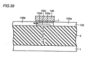
- the SOI-MOSFET is built at a semiconductor layer (hereinafter referred to as SOI layer) 105 deposited on a substrate 1 with an insulating layers 3 therebetween.
- SOI layer semiconductor layer
- the SOI-MOSFET is constituted of a drain region 105a and a source region 105b formed at SOI layer 105, and a gate electrode layer 109 placed on a region 105c (hereinafter referred to as channel formation region) between drain region 105a and source region 105b and opposite to channel formation region 105c with a gate insulating layer 7 therebetween.
- Drain region 105a and source region 105b of the SOI-MOSFET conventionally have a low breakdown voltage since the potential of SOI layer 105 (hereinafter conveniently referred to as body potential) is floating.
- n channel when voltage is applied to gate electrode layer 109 to form a channel at the surface of channel formation region 105c, electrons move from source region 105b toward drain region 105a. Impact ionization caused by the electrons generates a number of electron-hole pairs in the vicinity of the edge of drain region 105a. Although the electrons are removed from drain region 105a to the outside of SOI layer 105, the holes accumulate in SOI layer 105 because of the floating state of SOI layer 105.
- SOI layer 105 in such a state a positive voltage is applied thereto, and source/drain regions 105a and 105b and channel formation region 105c are forward biased. Accordingly, current easily flows between drain region 105a and source region 105b and source ⁇ drain breakdown voltage decreases.
- a proposed element isolation method for improving the source ⁇ drain breakdown voltage is field shield isolation (hereinafter referred to as FS isolation).
- Fig. 33 is a bird's eye view illustrating a structure of an SOI-MOSFET to which the FS isolation structure is applied.
- Fig. 34A is a schematic plan view of the MOSFET portion viewed in the direction of the arrow H of Fig. 33, and
- Fig. 34B is a schematic plan view along the F-F line of Fig. 34A.
- an SOI layer 105 is formed on a silicon substrate 1 with a buried insulating layer 3 interposed.
- an MOSFET constituted of source/drain regions 105a, 105b and a gate electrode layer 109 is formed at SOI layer 105.
- Gate electrode layer 109 extends in a region opposite to SOI layer 105 with a gate insulating layer 7 therebetween while keeping a prescribed gate length (Fig. 34A).
- the FS isolation structure is formed to have an FS plate 11 opposite to SOI layer 105 at an edge of the region where the MOSFET is formed with an intervening insulating layer. According to the method of isolating transistors by the FS isolation method, the potential of SOI layer 105 under FS plate 11 is fixed by applying a prescribed voltage to FS plate 11 for electrically isolating devices such as transistors that are adjacent to each other.
- the voltage applied to FS plate 11 is, for example, 0V for an nMOSFET, and Vcc (power supply voltage) for a pMOSFET.
- a body contact 23 for drawing out potential from SOI layer 105 is provided opposite to the MOSFET formation region with SOI layer 105 under FS plate therebetween.
- body fix an advantage specific to the SOI-MOSFET of a small substrate bias effect is lost. Further, a problem arises that an advantage of the SOI structure of high speed and low power consumption is decreased. The problem is hereinafter described in detail.
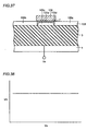
- Fig. 35 is a cross sectional view schematically showing a structure of a transistor formed at a normal semiconductor substrate (hereinafter referred to as bulk ⁇ transistor).
- the bulk ⁇ transistor includes a drain region 205a and a source region 205b formed to define a channel region 205e at a semiconductor substrate 201, and a gate electrode layer 209 formed on the region therebetween with an intervening gate insulating layer 207.
- substrate bias V B is applied to SOI layer 105 via a buried oxide film 3. Therefore, substrate bias V B has little effect on threshold voltage Vth. As shown in Fig. 38, threshold voltage Vth scarcely changes with substrate bias V B .
- threshold voltage Vth increases as described above, drain current Id decreases to make it difficult to operate an LSI (Large Scale Integrated Circuit) at a high speed.
- the high threshold voltage Vth prevents reduction of supply voltage, and power consumption increases
- a semiconductor device in form of a SOI MOSFET comprising a semiconductor layer placed on a substrate with an insulating layer therebetween, a gate insulation type field effect transistor including a pair of source/drain region placed at said semiconductor layer spaced from each other and a gate electrode layer which is opposite to a channel formation region with a gate insulating layer interposed, said channel formation region sandwiched between the paired source/drain regions, and forming a channel in said channel formation region by controlling potential of said gate electrode layer, and an isolation conductive layer electrically insulated from said semiconductor layer, wherein said gate insulation type field effect transistor can be electrically isolated from other elements by controlling potential of said isolation conductive layer to fixed potential of a region of said semiconductor layer opposite to said isolation conductive layer, potential can be applied to said channel formation region from a prescribed region via the region of said semiconductor layer opposite to said isolation conductive layer.
- One object of the present invention is to provide a semiconductor device having an excellent source ⁇ drain breakdown voltage as well as a small substrate bias effect operating at high speed and with low power consumption, and a method of manufacturing such a semiconductor device.
- a semiconductor device according to the present invention is defined in claims 1, 5 and 9.
- the semiconductor device of the present invention is structured such that a region at the edge of the channel formation region is completely depleted before the central portion thereof is depleted when voltage is applied to the gate. If the region at the edge is completely depleted prior to depletion of the central portion, subsequent application of the body potential to the central portion is blocked. Accordingly, extension of a depletion layer at the junction of the source/drain regions and the semiconductor layer in the central portion is prevented, so that threshold voltage Vth can be reduced. Since threshold voltage Vth decreases, drain current Id increases to easily implement high speed operation of the LSI. Further, reduction of threshold voltage Vth provides a reduced supply voltage and thus a reduced power consumption.
- the opposite region is preferably located at the edge portion of,the channel formation region.
- an area of a cross section of the channel formation region in the direction of the channel length defined by (sandwiched between) the front and back surfaces of the semiconductor layer is preferably smaller at the edge portion than at the central portion.
- the edge portion By making the cross sectional area of the edge portion different from that of the central portion, the edge portion can be completely depleted prior to depletion of the central portion. As a result, a gate insulation type field effect transistor which is superior in the source ⁇ drain breakdown voltage, has a small substrate bias effect, and operates at high speed with low power consumption can be obtained.
- a channel length at the edge portion of the channel formation region is preferably smaller than a channel length at the central portion of the channel formation region.
- edge portion and the central portion in the direction of the channel length are different from each other, the edge portion can be completely depleted prior to depletion of the central portion. Consequently, a gate insulation type field effect transistor which is superior in the source ⁇ drain breakdown voltage, has a small substrate bias effect, and operates at high speed with low power consumption can be obtained.
- a gate length of the gate electrode layer is preferably smaller at a location opposite to the edge portion than at a location opposite to the central portion.
- the edge portion and the central portion different from each other in the width in the direction of the channel length can be easily formed by injecting impurities into the semiconductor layer with the gate electrode as a mask.
- the edge portion has a region where a thickness of the semiconductor layer is smaller than that at the central portion.
- the edge portion can be completely depleted prior to depletion of the central portion.
- a gate insulation type field effect transistor having a superior source ⁇ drain breakdown voltage and a small substrate bias effect, and operating at high speed with low power consumption can be obtained.
- a trench having a depth of at least 10 nm, (100 ⁇ ), (1 nm 10 Angström), is formed at the front or back surface of the semiconductor layer.
- the depth of the trench is less than 100 ⁇ , the effect of the complete depletion of the edge portion preceding the central portion cannot be sufficiently achieved.
- the source/drain region has a first impurity region of a relatively high concentration and a second impurity region of a relatively low concentration adjacent to the first impurity region on the channel formation region side.
- the width in the channel length direction of the second impurity region adjacent to the edge portion is larger than that of the second impurity region adjacent to the central portion.
- the second impurity region has a width larger at the edge portion than at the central portion.
- the second impurity region has a high parasitic resistance since the concentration of the impurities therein is relatively small. Therefore, when the transistor is turned on, current chiefly flows in the central portion having a narrow width of the second impurity region and a low parasitic resistance. In other words, the current hardly flows in the edge portion having a narrow width in the channel length direction, and an insulation gate type field effect transistor which is immuned to the short channel effect can be obtained.
- a reflection film having a shape which is matched to that of the gate electrode layer is preferably formed on the gate electrode layer.
- the reflection film is provided on the gate electrode layer, a resist region corresponding to the top of the edge portion can be exposed excessively by irregular reflection of exposure light from the reflection film when the gate electrode layer is exposed for patterning thereof. Accordingly, the gate electrode layer having its length smaller at the edge portion than at the central portion can be formed without changing a gate electrode pattern of a photomask, and the manufacturing process can be simplified.
- a method of manufacturing a semiconductor device is defined in claim 10. .
- the edge portions and the central portion having different widths in the channel length direction can be easily formed by injecting impurities into the semiconductor layer using the gate electrode as a mask.
- the step of forming the gate electrode layer includes a step of exposing a photoresist applied to a conductive layer with exposure light transmitted through a photomask having a gate electrode pattern, followed by developing to form a resist pattern and etching of the conductive layer using the resist pattern as a mask.
- a location corresponding to an edge portion of the gate electrode pattern there is a gap having a width smaller than the limit of resolution of a conventional stepper and isolating the gate electrode pattern.
- the conductive layer is patterned by the photolithography with a reflection film formed on the conductive layer corresponding to the gate electrode layer.
- the reflection film is formed on the gate electrode layer, a resist region corresponding to the top of the edge portion can be exposed excessively by irregular reflection of exposure light from the reflection film when the gate electrode layer is exposed for patterning. Therefore, the gate electrode layer having its length smaller at the edge portions than at the central portion can be obtained without changing the shape of the gate electrode pattern of the photomask, and the manufacturing process can be simplified.
- a step is further provided by which an insulating layer is formed to cover the gate electrode layer, and the insulating layer is left at a sidewall of the gate electrode layer by anisotropically etching the insulating layer.
- the region of the gate electrode layer having a small gate length located on the edge portion is provided to have a prescribed width in the direction of the gate width.
- the thickness of the insulating layer when it is formed is at least two times larger than the prescribed width.
- an insulation gate type field effect transistor having its edge portion which is immuned to the short channel effect can be obtained.
- the step of forming the gate electrode layer includes a step of exposing a photoresist applied onto the conductive layer with exposure light transmitted through a photomask having a gate electrode pattern, forming a resist pattern through development, and etching the conductive layer using the resist pattern as a mask.
- a first line width located correspondingly to the edge portion of the gate electrode pattern is smaller than a second line width located correspondingly to the central portion of the gate electrode pattern.
- a line width located correspondingly to a region sandwiched between the edge portion and the central portion of the gate electrode pattern is larger than the second line width.
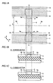
- Fig. 1A is a plan view schematically showing a structure of a semiconductor device according to the first embodiment of the invention.
- Fig. 1B is a schematic cross sectional view along the B-B line of Fig.1A.
- Fig. 1C is a schematic cross sectional view along the C-C line of Fig. 1A.
- Figs. 2-7 are schematic cross sections corresponding to the A-A line of Fig. 1A showing a method of manufacturing the semiconductor device according to the first embodiment of the invention in the order of steps.
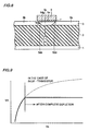
- Fig. 8 is a schematic cross sectional view provided for describing depletion of a region sandwiched between source/drain regions of an SOI-MOSFET.
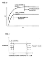
- Fig. 9 is a graph showing a relation between substrate bias V B and threshold value Vth when a region sandwiched between source/drain regions of an SOI-MOSFET is completely depleted.
- Fig. 10 is a graph showing a relation between substrate bias V B and threshold voltage Vth when the gate length of an SOI-MOSFET varies.
- Fig. 11 is a graph showing change of the potential of a semiconductor layer along the A-A line of Fig. 1A when a narrowed portion is completely depleted.
- Fig. 12 is a graph showing a relation between substrate bias V B and source ⁇ drain breakdown voltage BV DS when a narrowed portion is completely depleted.
- Fig. 13 and Fig. 14 are schematic cross sectional views along the A-A line of Fig. 1A showing a method of manufacturing a semiconductor device according to the second embodiment of the invention in the order of steps.
- Fig. 15 is a graph showing a relation between a size of a step of an FS portion and reduction of a pattern width when there is a reflection film on a gate electrode layer and when there is no reflection film thereon.
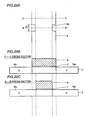
- Fig. 16 is a schematic plan view showing a shape of a gate electrode pattern of a photomask used for forming a gate electrode layer of a semiconductor device according to the third embodiment of the invention.
- Fig. 17 is a schematic plan view showing a shape of a gate electrode layer when the gate electrode layer is formed using the photomask having the pattern shown in Fig. 16.
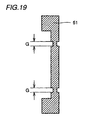
- Fig. 18 and Fig. 19 are schematic plan views showing various shapes of a gate electrode pattern of a photomask when a gate electrode layer of a semiconductor device according to the fourth embodiment of the invention is formed.
- Fig. 20 and Fig. 21 are schematic plan views showing a method of manufacturing a semiconductor device according to the fifth embodiment of the invention in the order of steps.
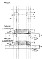
- Fig. 22A is a schematic plan view showing a narrowed portion of a gate electrode layer of a semiconductor device according to the sixth embodiment of the invention by enlarging it.
- Fig. 22B is a schematic cross section along the C-C line of Fig. 22A.
- Fig. 22C is a schematic cross section along the B-B line of Fig. 22A.
- Fig. 23A is a schematic plan view showing that a sidewall insulating layer of the semiconductor device of the sixth embodiment of the invention is formed.
- Fig. 23B is a schematic cross section along the C-C line of Fig. 23A.
- Fig. 23C is a schematic cross section along the B-B line of Fig. 23A.
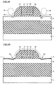
- Figs. 24-26 are partial schematic cross sections along the A-A line of Fig. 1A showing a method of manufacturing a semiconductor device according to the seventh embodiment of the invention in the order of steps.
- Fig. 27 is a schematic plan view of a mask and a gate electrode showing that a narrowed portion of the gate electrode cannot be successfully buried by sidewalls.
- Fig. 28 and Fig. 29 are schematic plan views of a mask and a gate electrode showing that a narrowed portion of a gate electrode layer can be successfully buried by sidewalls of a semiconductor device according to the eighth embodiment of the invention.
- Fig. 30 is a plan view schematically showing a structure of a semiconductor device according to the ninth embodiment of the invention.
- Fig. 31 is a schematic cross section corresponding to the cross section along the D-D line of Fig. 30 showing mesa isolation of a semiconductor layer of a semiconductor device according to the tenth embodiment of the invention.
- Fig. 32 is a cross sectional view schematically showing a structure of a conventional SOI-MOSFET.
- Fig. 33 is a bird's eye view schematically showing a structure of a conventional SOI-MOSFET to which FS separation is applied.
- Fig. 34A is a schematic plan view viewed in the direction of the arrow E of Fig. 33.
- Fig. 34B is a schematic cross section along the F-F line of Fig. 34A.
- Fig. 35 is a schematic cross section provided for describing a substrate bias effect of a bulk ⁇ transistor.
- Fig. 36 is a graph showing a relation between substrate bias V B and threshold voltage Vth of the bulk ⁇ transistor of Fig. 35.
- Fig. 37 is a cross section schematically showing a structure of an SOI-MOSFET to which substrate bias is applied via a buried insulating layer.
- Fig. 38 is a graph showing a relation between substrate bias V B and threshold voltage Vth of a transistor when the substrate bias is applied via a buried insulating layer.
- Fig. 39 is a cross sectional view schematically showing a structure of a body-fixed SOI-MOSFET.
- Fig. 1A is a plan view schematically showing a structure of a semiconductor device according to the first embodiment of the present invention.
- Figs. 1B and 1C are schematic cross sections along the B-B line and C-C line of Fig. 1A.
- a semiconductor device of this embodiment has what is called SOI structure where an SOI layer 5 is formed on a silicon substrate 1 with a buried oxide film 3 therebetween.
- An SOI-MOSFET is formed at SOI layer 5.
- the SOI-MOSFET includes a drain region 5a and a source region 5b arranged to sandwich a channel formation region 5c at SOI layer 5, and a gate electrode layer 9 opposite to channel formation region 5c with a gate oxide film 7 therebetween.
- an FS plate 11 is formed opposite to SOI layer 5 with an insulating layer (not shown) therebetween.
- FS isolation having FS plate 11 electrically isolates the SOI-MOSFET from other elements such as an adjacent transistor.
- isolation is achieved by applying a prescribed potential to FS plate 11 to fix the potential of SOI layer 5 under FS plate 11 as described above.
- Channel formation region 5c includes two edge portions J on both sides in the direction of the channel width (direction of arrow Y) of the SOI-MOSFET, and a central portion K sandwiched between edge portions J and extending with a prescribed width (channel length) maintained.
- channel formation region 5c has a region of a width (channel length) in a direction of the channel length (direction of arrow X) smaller than that of the central portion K (see Fig. 1B: hereinafter referred to as narrowed portion).
- Gate electrode layer 9 also extends with a prescribed width (gate length) maintained on central portion K, and has a narrowed portion 9a having a width (gate length) in a direction of the gate length (direction of arrow X) smaller on the narrowed portion of channel formation region 5c than on the central portion K.
- a prescribed potential is applied via a region under FS plate 11 from a prescribed region (body contact 23) outside the region where MOSFET is formed as shown in Fig. 33.
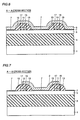
- Figs. 2-7 are schematic cross sections along the A-A line of Fig. 1A showing the method of manufacturing the semiconductor device of the first embodiment of the invention in order of steps.
- a wafer of the SOI structure having SOI layer 5 on silicon substrate 1 with buried oxide film 3 therebetween is prepared.
- an insulating film 15 under the FS plate, a conductive layer 11 to be the FS plate, and insulating film 17 on the FS plate are successively formed with respective thicknesses of 20 nm, 50 nm and 100 nm.
- conductive layer 11 to be the FS plate for example, a polycrystal silicon film which has already doped with impurities when deposited (doped polysilicon) may be used, or a polycrystal silicon film which is not doped with impurities (non-doped polysilicon) and to which impurities are injected after deposited may be used.
- insulating films 15 and 17 on and under the FS plate for example, a silicon oxide film (SiO 2 ), a silicon nitride film (SiN) or a composite film of them is used.
- FS plate 11 by normally used photolithography and etching, FS plate 11, and insulating films 15 and 17 on and under the FS plate are left by patterning at a location where the FS isolation is provided.
- a sidewall insulating layer 13 is formed at a sidewall of an FS isolation structure (including FS plate 11 and insulating films 15 and 17 on and under FS plate 11). Sidewall insulating layer 13 is formed to remain at the sidewall of the FS isolation structure by an anisotropic dry etching of a silicon oxide film deposited with a thickness of approximately 200 nm, for example.
- a gate oxide film 7 is formed at the surface of semiconductor layer 5 with a thickness of approximately 7 nm by thermal oxidation, for example.
- a polysilicon layer 9 to be a gate electrode layer is deposited on the entire surface with a thickness of 250 nm, for example.
- a doped polysilicon to which impurities have been injected already when deposited may be used, or a non-doped polysilicon doped with impurities after deposited may be used.
- gate electrode layer 9 is formed by patterning according to normal photolithography and etching of polysilicon layer 9. At this time, gate electrode layer 9 is patterned to have a narrowed portion in the vicinity of the FS isolation structure as shown in Fig. 1A. A pair of source/drain regions is formed by ion injection of impurities into SOI layer 5 using gate electrode layer 9 and the FS isolation structure as a mask. Accordingly, a narrowed portion at the edge of the channel formation region sandwiched between the source and drain regions is formed to match the narrowed portion of gate electrode layer 9.
- a photoresist on gate electrode layer 9 may be patterned using a photomask (reticle) having a gate electrode pattern with a narrowed portion at a corresponding location, and the conductive layer to be gate electrode layer 9 may be patterned using the resist pattern as a mask in order to form gate electrode layer 9 having the narrowed portion.
- a photomask reticle
- the semiconductor device of this embodiment has a narrowed portion at the edge portion J of channel formation region 5c as described above. Therefore, the semiconductor device has a superior source ⁇ drain breakdown voltage and a small substrate bias effect, and operates at high speed and with low power consumption. This is described in detail below.
- threshold voltage Vth increases with substrate bias V B similarly to the case of the bulk ⁇ transistor (Fig. 35, Fig. 36). However, if substrate bias V B is further increased, channel formation region 5c is entirely depleted (complete depletion) by a depletion layer 5dd extending from drain region 5a, a depletion layer 5ds extending from source region 5b, and a depletion layer 5dg extending from gate electrode layer 9. Even if substrate bias V B is increased to reach substrate bias V B or more causing the complete depletion, threshold voltage Vth is not affected by substrate bias V B and does not increase (saturated).
- depletion layer 5dg extends deeper compared with the case in which only depletion layer 5dg is present since depletion layer 5dg is sandwiched between depletion layers 5dd and 5ds extending from drain region 5a and source region 5b respectively and affected by them.
- depletion layers 5dd and 5ds extending respectively from drain region 5a and source region 5b on depletion layer 5dg extending from gate electrode layer 9 is greater as the gate length is decreased. Therefore, if the thickness of SOI layer 5 is constant, channel formation region 5c is completely depleted faster as the channel length is smaller, and substrate bias V B when threshold voltage Vth is saturated is smaller.
- Fig. 10 shows change of threshold voltage Vth for two cases in which the thickness of SOI layer 5 is the same and the channel length is large and small. As clearly understood by Fig. 10, channel formation region 5c is completely depleted by a smaller substrate bias V B as the channel length is smaller.
- the channel length at the narrowed portion of the edge portion J of channel formation region 5c is smaller than the channel length at the central portion K. Therefore, when substrate bias V B is applied from the body contact, edge portion J is completely depleted preceding depletion of central portion K by a low substrate bias V B . Even if substrate bias V B higher than that us applied, potential from body contact is not transmitted into central portion K of prescribed region 5c. In other words, the potential from the body contact is blocked by the completely depleted edge portion J.
- threshold voltage Vth can be decreased. Since the threshold voltage Vth is decreased, drain current Id increases and high speed operation of an LSI is easily implemented. Further, reduction of supply voltage and power consumption is possible since threshold voltage Vth can be reduced.
- Fig. 11 is a graph showing change of the potential at the bottom portion of the SOI layer corresponding to the cross ection of the A-A line of Fig. 1.
- position a 1 and position a 2 correspond to those shown in Fig. 1.
- the central portion is located in the region between positions a 1 and a 2
- the narrowed portion of the channel formation region is located on the opposite side of the central portion in relation to positions a 1 and a 2 .
- carriers in central portion K move from central portion K to the body contact to some extent by diffusion or recombination even after the narrowed portion is completely depleted. It also contributes to prevention of decrease of the source ⁇ drain breakdown voltage in this embodiment compared with the case in which the SOI layer is completely floating.
- an SOI-MOSFET having a superior source ⁇ drain breakdown voltage and a small substrate bias effect, and operating at high speed and with low power consumption can be obtained.
- narrowed portions are formed at edge portions on both sides of central portion K in this embodiment, the narrowed portion may be formed at one location if the potential from the body contact can be blocked. For example, if the body contact is provided on one side only, the narrowed portion may be provided at one location on the body contact side.
- the second embodiment relates to a method of forming a gate electrode layer having a narrowed portion without changing the conventional shape of the gate electrode pattern of the photomask.
- Figs. 13 and 14 are schematic cross sections along the A-A line of Fig. 1 showing a method of manufacturing a semiconductor device according to the second embodiment of the invention in order of steps.
- the manufacturing method according to this embodiment has manufacturing steps similar to those of the first embodiment shown in Figs. 2-6.
- a reflection film 21 for enhancing reflection intensity is formed at the entire surface of a conductive layer 9 which is to be a gate electrode layer.
- a photoresist 31 of the positive type for example, is applied onto the entire surface of reflection film 21.
- Photoresist 31 is irradiated by exposure light 30 which is passed through a photomask from a stepper.
- Reflection film 21 covers a step portion of the FS isolation structure and causes irregular reflection of exposure light 30 at a step portion of a sidewall of reflection film 21. This irregular reflection increases the intensity of the exposure light at region S 1 in the vicinity of a step portion of photoresist 31.
- the positive photoresist is removed by development in a region which is irradiated by the light, so that photoresist 31 is excessively removed in the vicinity of region S 1 where the intensity of the exposure light is high, and the shape of the resist pattern in the vicinity of region S 1 is narrowed.
- a gate electrode layer 9 having a narrowed portion on the edge portion of channel formation region is thus formed by etching reflection film 21 and conductive layer 9 using resist pattern 31 as a mask.
- the channel length at the edge portion of the channel formation region sandwiched between the source and drain regions becomes smaller than that at the central portion.
- the gate electrode layer and the channel formation region each having the narrowed portion at the edge portion can be formed using a gate pattern shape of a conventional photomask, by providing reflection film 21 on conductive layer 9 that is to be the gate electrode layer.
- Reflection by reflection film 21 is determined by the wavelength of exposure light, the thickness and refractive index of reflection film 21.
- the material of reflection film 21 is a silicon nitride film
- refractive index n of reflection film 21 for a resist is 1.4
- i-line wavelength:365 nm
- the result clearly shows that the pattern can be narrowed further with reflection film 21 than without reflection film 21 if height H FS of the field shield isolation structure is the same.
- gate electrode layer 9 having a gate length which is sufficiently small at the narrowed portion can be obtained by providing reflection film 21 even if height H FS of the field shield isolation structure is decreased.
- the pattern can be narrowed even if the reflection film is not provided, by increasing height H FS of the FS isolation structure, a step at the surface increases to cause problems of disconnection of a conductive layer formed thereon, short circuit due to residue, and the like.
- the third embodiment relates to a method of forming a gate electrode layer having a minute gate length on a narrowed portion by manipulation of a gate electrode pattern of a photomask.
- Fig. 16 is a schematic plan view showing a structure of the gate electrode pattern of the photomask for patterning a gate electrode layer of a semiconductor device according to the third embodiment of the invention.
- a gate electrode pattern 51 has a gap G having resolution equals to or smaller than that of a stepper, at a location corresponding to a narrowed portion of a channel formation region.
- the gap portion of gate electrode pattern 51 disappears due to the proximity effect.
- gate electrode layer 9 having its width narrower at the portion where the gap was present than at other portions can be obtained as shown in Fig. 17.
- Gate electrode layer 9 is patterned using gate electrode pattern 51 having gap G, and a narrowed portion having a minute gate length can be formed.
- Figs. 18 and 19 are schematic plan views each showing a structure of a gate electrode pattern of a photomask for patterning a gate electrode layer of a semiconductor device according to the fourth embodiment of the invention.
- a gate electrode pattern 51 of a photomask may have a narrowed portion formed instead of a gap at a location corresponding a narrowed portion of a channel formation region.
- the shape of a notch to form the narrowed portion may be triangle (Fig. 18) or rectangular (Fig. 19) as shown in Figs. 18 and 19.
- the shape of the notch region is not limited to those shapes, and may be polygonal or a curved shape.
- This embodiment relates to a structure which has a narrowed portion at a channel region but which is immune to short channel effect.
- Fig. 20 is a plan view schematically showing a structure of a semiconductor device according to the fifth embodiment of the invention.
- n - impurity regions 5d of relatively low concentration are formed on both sides of a narrowed portion of a channel formation region located under a gate electrode layer 9.
- n + impurity regions 5a and 5b of relatively high concentration are formed on both sides of a central portion of the channel formation region.
- n - impurity region 5d increases parasitic resistance. Therefore, current flowing between the source/drain when a transistor is turned on chiefly flows between n + impurity regions 5a and 5b, and scarcely flows between n- impurity regions 5d on both sides of the narrowed portion.
- Fig. 21 is a schematic plan view showing a method of manufacturing the semiconductor device according to the fifth embodiment of the invention. According to the method of manufacturing of this embodiment, a step of forming gate electrode layer 9 and preceding steps shown in Fig. 2 to Fig. 7 are executed. Ion implantation of n-type impurities is carried out using gate electrode layer 9, an FS isolation structure, and the like as a mask, and an n- impurity region is formed at an SOI layer.
- a resist pattern 33 is formed on the insulating layer to cover at least a narrowed portion of gate electrode layer 9 and portions on both sides thereof, and the underlying insulating layer is anisotropically etched using resist pattern 33 as a mask. Consequently, a sidewall insulating layer (not shown) covering the narrowed portion and the portions on both sides of gate electrode layer 9 and covering a sidewall of gate electrode layer 9 is formed.
- N + impurity regions 5a and 5b are formed by ion implantation of n-type impurities using the sidewall insulating layer, gate electrode layer 9, the FS isolation structure and the like as a mask. As a result, the semiconductor device of Fig. 20 is obtained.
- portions on both sides of the narrowed portion of the channel formation region are covered with the same film (e.g. SiO 2 ) as that of the sidewall insulating layer of gate electrode layer 9. Therefore, even if silicidation processing causes silicidation of the surface of n + impurity region 5a, silicidation of the surface of n + impurity region 5d never occurs. Accordingly, the resistance of n- impurity region 5d is not reduced by the silicidation and the problem of the short channel effect caused by the reduced resistance is avoided.
- the same film e.g. SiO 2
- N + impurity regions 5a and 5b may be formed by providing a sidewall insulating layer covering a sidewall of gate electrode layer 9, forming resist pattern 33 as shown in Fig. 21 and injecting n-type impurities after formation of n - impurity region 5d.
- This method is applicable to a pMOSFET if the conductivity type is reversed to change n + to p + and n - to p - .
- This embodiment is a modification of the fifth embodiment and does not require an additional photomask.
- Fig. 22A and Fig. 23A are schematic plan views each illustrating an enlarged narrowed portion of a gate electrode layer, showing a method of manufacturing a semiconductor device of the sixth embodiment of the invention in order of steps.
- Figs. 22B and 22C are schematic cross sections respectively along the C-C line and B-B line of Fig. 22A.
- Figs. 23B and 23C are schematic cross sections along the C-C line and B-B line respectively of Fig. 23A.
- n - impurity regions 5a 1 and 5b 1 to be a drain region and a source region are formed at an SOI layer 5 by injection of n-type impurities using a gate electrode layer 9 and the like as a mask.
- an insulating layer 19 is formed to cover the entire surface.
- the thickness of insulating layer 19 is at least 1/2 of the maximum width G of a narrowed portion 9a of gate electrode layer 9.
- a sidewall insulating layer 19 covering a sidewall of gate electrode layer 9 is formed by anisotropically dry etching insulating layer 19.
- N + impurity regions 5a 2 and 5b 2 are formed at SOI layer 5 by injection of n-type impurities using gate electrode layer 9, sidewall insulating layer 19 and the like as a mask.
- a drain region 5a of an LDD (Lightly Doped Drain) structure is formed of n - impurity region 5a 1 and n + impurity region 5a 2
- a source region 5b of the LDD structure is formed of n impurity region 5b 1 and n + impurity region 5b 2 .
- Insulating layer 19 is formed with its thickness of at least 1/2 of the maximum width G of narrowed portion 9a, so that the shape of the plane of sidewall insulating layer 19 formed of insulating layer 19 is almost in a straight line and a narrowed portion is not generated correspondingly to narrowed portion 9a.
- N + impurity regions 5a 2 and 5b 2 are formed using sidewall insulating layer 19 and the like as a mask, so that the widths in the channel length direction of n + impurity regions 5a 1 and 5b 1 is larger at the cross section of narrowed portion 9a (Fig. 23C) than at the cross section of the central portion (Fig. 23B).
- n - impurity regions 5a 1 and 5b 1 in the channel length direction on both sides of narrowed portion 9a are larger to increase parasitic resistance of n - impurity regions 5a 1 and 5b 1 . Therefore, current chiefly flows in a portion other than narrowed portion 9a of the central portion when a transistor is turned on. The transistor is thus never easily affected by the short channel effect. According to this embodiment, an SOI-MOSFET which is immuned to the punch-through is obtained without increasing the number of masks for transistor formation.
- sidewall insulating layer 19 should be made thinner, there is a method of reducing the width of the sidewall insulating layer by wet etching or the like, after forming an insulating film 19 with a thickness of at least 1/2 of the maximum width G of narrowed portion 9a and burying narrowed portion 9a as described above.
- the narrowed portion having a small width in the channel length direction is provided to channel formation region 5c to cause complete depletion of the narrowed portion prior to depletion of any other portion (central portion).
- a technique for completely depleting a part of an SOI layer prior to depletion of other parts by reducing the thickness of the part of the SOI layer to be smaller than that of the other parts.
- Figs. 24-26 are partial schematic cross sections along the A-A line of Fig. 1A showing a method of manufacturing a semiconductor device according to the seventh embodiment of the invention in order of steps.
- steps similar to those of the first embodiment shown in Figs. 2-4 are carried out.
- overetch of at least 50% is performed when anisotropic etching is applied for forming a sidewall insulating layer 13 constituted of a silicon oxide film.
- the etch selectivity (SiO 2: Si) when the anisotropic etching is carried out is approximately 10:1.
- insulating layer 13 for forming sidewall insulating layer 13 is fabricated with a thickness of 2000 A, a trench R 2 having its depth T of at least 100 ⁇ is formed at SOI layer 5 by overetch of 50% carried out for forming sidewall insulating layer 13.
- SOI layer 5 at the edge of the FS isolation is especially deeply overetched to be removed. This is caused by a characteristic that the plasma as the etchant of dry etching concentrates at region R 1 above the edge portion.
- Overetch of anisotropic etching for formation of normal sidewall insulating layer 13 is approximately 10%. Therefore, depth T of trench R 2 formed at SOI layer 5 is normally about 20 ⁇ at most.
- depth T of trench R 2 may be increased by setting the etch rate of SOI layer 5 and sidewall insulating layer 13 to values dose to each other.
- the etch selectivity of sidewall insulating layer 13 and SOI layer 5 may be changed only for the vicinity of the end point of etching for formation of sidewall insulating layer 13.
- trench R 2 is separated from the edge of sidewall insulating layer 13 by applying wet etching to recess sidewall insulating layer 13 and an insulating layer 17 covering an FS plate 11 to a some degree.
- a gate insulating layer 7 is thereafter formed at the surface of SOI layer 5 by thermal oxidation process or the like.
- trench R 2 When trench R 2 is located near the edge of sidewall insulating layer 13 as shown in Fig. 24, stress is likely to concentrate at this portion when gate insulating layer 7 is formed. This may cause leakage current. Therefore, trench R 2 is preferably separated from the edge of sidewall insulating layer 13.
- a gate electrode layer 9 is formed to be opposite to SOI layer 5 with gate insulating layer 7 therebetween.
- the film thickness of SOI layer 5 is partially reduced by providing trench R 2 at a part as described above. As a result, the region having a smaller thickness located at the edge of the channel formation region is first depleted completely when substrate bias is applied, and application of the substrate bias to the central portion is prevented. Increase of threshold voltage of a transistor can be avoided accordingly.
- the body fix is possible via SOI layer 5 under FS plate 11.
- This embodiment relates to a modification of the sixth embodiment.
- a narrowed portion 9ab of a gate electrode layer 9b on the wafer has a blurred shape.
- the shape of an opening end R 31 of narrowed portion 9ab is blurred, and width G of narrowed portion 9ab is substantially increased. Therefore, a narrowed portion of a sidewall insulating layer 19 formed at a sidewall of gate electrode layer 9b tends to be produced at a location corresponding to narrowed portion 9ab of gate electrode layer 9b.
- a transistor is easily affected by the short channel effect as described above.
- a wide portion 52c is provided in the vicinity of the end of the opening of a narrowed portion 51ac of a gate electrode pattern 51c of a photomask as shown in Fig. 28.
- Wide portion 52c has width W1 larger than length W2 of another region.
- narrowed portion 9ac can be successively buried at a sidewall insulating layer 19.
- the length of a wide portion 52d may be extremely increased as shown in Fig. 29. It is only necessary that length W3 of sidewall insulating layer 19 covering narrowed portion 9ad of gate electrode layer 9d is formed to be smaller than length W4 of the main portion of gate electrode layer 9d.
- This embodiment is not limited to the case in which the notch regions forming the narrowed portion are provided on both sides of the gate electrode layer, but is applicable to a case in which a notch region is provided on one side of the gate electrode layer.
- this embodiment can be applied to either an nMOSFET or a pMOSFET.
- This embodiment relates to a structure that achieves both of body fixing and reduction of the substrate bias effect without thinning a gate electrode layer and without thinning an SOI layer.
- Fig. 30 is a plan view schematically showing a structure of a semiconductor device according to the ninth embodiment of the invention.
- an SOI layer 55 is isolated like mesa (mesa isolation), or isolated by a field oxide film according to LOCOS (Local Oxidation of Silicon) to be formed into a prescribed shape.
- SOI layer 55 has an almost fixed width at a region where a drain region 55a and a source region 55b are formed, and includes an extended portion 55d electrically connected to a channel formation region 55c between drain region 55a and source region 55b and extending to the outside of a region where a transistor is formed.
- a body contact 23 is formed at a leading end of extended portion 55d.
- an FS plate 11 is opposite via an insulating layer (not shown).
- a gate electrode layer 9 which is opposite to channel formation region 55c with a gate insulating layer therebetween extends over FS plate 11 and is opposite to a region 55e of extended portion 55d, sandwiched between the region to which body contact 23 is connected and the region opposite to FS plate 11, via an insulating layer.
- Region 55e has an impurity concentration lower than that of another region of extended portion 55d and that of channel formation region 55c.
- a thin portion is not necessary at a part of channel formation region 55c. Therefore, the device is not easily affected by punch-through.
- capacitance between gate electrode layer 9 and FS plate 11 could be increased since gate electrode layer 9 extends over FS plate 11. If it causes a serial problem, the capacitance can be reduced by removing FS plate 11 and using a structure of oxide film isolation formed of only oxide films over and under FS plate 11 and a sidewall.
- This embodiment relates to a modification of the ninth embodiment.
- Fig. 31 is a schematic cross section along the D-D line of Fig. 30.
- this embodiment relates to mesa isolation of SOI layer 55 of the ninth embodiment.
- gate electrode layer 9 can cover not only the top surface of region 55e but both side surfaces thereof.
- a depletion layer can be extended from the three surfaces (top surface and both side surfaces) to region 55e by gate electrode layer 9, so that complete depletion can be achieved more speedily and the influence of the substrate bias effect can be reduced further when substrate bias is applied.
- the semiconductor device of the present invention has a structure which allows a region on the body contact side to be completely depleted prior to depletion of a central portion. Specifically, the cross sectional area of the edge portion of the channel formation region is made smaller than that of the central portion, or the impurity concentration of a region closer to the body contact than the central portion is made lower than that of the central portion.
- the cross sectional area of the channel formation region refers to a cross section in the direction of the channel length of the channel formation region, the section sandwiched between the front surface and the back surface of the SOI layer.
- the present invention can be applied advantageously to a structure of an SOI-MOSFET having the FS isolation structure and a method of manufacturing the same.
Landscapes
- Engineering & Computer Science (AREA)
- Physics & Mathematics (AREA)
- Condensed Matter Physics & Semiconductors (AREA)
- General Physics & Mathematics (AREA)
- Manufacturing & Machinery (AREA)
- Computer Hardware Design (AREA)
- Microelectronics & Electronic Packaging (AREA)
- Power Engineering (AREA)
- Thin Film Transistor (AREA)
Applications Claiming Priority (1)
| Application Number | Priority Date | Filing Date | Title |
|---|---|---|---|
| PCT/JP1996/003369 WO1998022983A1 (en) | 1996-11-15 | 1996-11-15 | Semiconductor device and process for manufacturing the same |
Publications (3)
| Publication Number | Publication Date |
|---|---|
| EP0948057A1 EP0948057A1 (en) | 1999-10-06 |
| EP0948057A4 EP0948057A4 (show.php) | 1999-10-06 |
| EP0948057B1 true EP0948057B1 (en) | 2002-10-16 |
Family
ID=14154104
Family Applications (1)
| Application Number | Title | Priority Date | Filing Date |
|---|---|---|---|
| EP96938489A Expired - Lifetime EP0948057B1 (en) | 1996-11-15 | 1996-11-15 | Semiconductor device and process for manufacturing the same |
Country Status (4)
| Country | Link |
|---|---|
| EP (1) | EP0948057B1 (show.php) |
| KR (1) | KR100287399B1 (show.php) |
| DE (1) | DE69624386T2 (show.php) |
| WO (1) | WO1998022983A1 (show.php) |
Families Citing this family (3)
| Publication number | Priority date | Publication date | Assignee | Title |
|---|---|---|---|---|
| KR100626009B1 (ko) | 2004-06-30 | 2006-09-20 | 삼성에스디아이 주식회사 | 박막 트랜지스터 구조체 및 이를 구비하는 평판디스플레이 장치 |
| JP4826127B2 (ja) * | 2005-04-25 | 2011-11-30 | ソニー株式会社 | 固体撮像装置及びその製造方法 |
| KR100722106B1 (ko) * | 2006-06-09 | 2007-05-25 | 삼성에스디아이 주식회사 | 박막 트랜지스터 및 그 제조방법 |
Family Cites Families (4)
| Publication number | Priority date | Publication date | Assignee | Title |
|---|---|---|---|---|
| JP2507567B2 (ja) * | 1988-11-25 | 1996-06-12 | 三菱電機株式会社 | 絶縁体基板上の半導体層に形成されたmos型電界効果トランジスタ |
| JP2547663B2 (ja) * | 1990-10-03 | 1996-10-23 | 三菱電機株式会社 | 半導体装置 |
| JP2636963B2 (ja) * | 1990-11-28 | 1997-08-06 | 三菱電機株式会社 | 半導体装置 |
| JPH08125187A (ja) * | 1994-10-24 | 1996-05-17 | Nippon Telegr & Teleph Corp <Ntt> | Soi構造mos型半導体装置およびその製造方法 |
-
1996
- 1996-11-15 KR KR1019980710963A patent/KR100287399B1/ko not_active Expired - Fee Related
- 1996-11-15 DE DE69624386T patent/DE69624386T2/de not_active Expired - Fee Related
- 1996-11-15 EP EP96938489A patent/EP0948057B1/en not_active Expired - Lifetime
- 1996-11-15 WO PCT/JP1996/003369 patent/WO1998022983A1/ja not_active Ceased
Also Published As
| Publication number | Publication date |
|---|---|
| KR20000022518A (ko) | 2000-04-25 |
| KR100287399B1 (ko) | 2001-05-02 |
| WO1998022983A1 (en) | 1998-05-28 |
| DE69624386D1 (de) | 2002-11-21 |
| EP0948057A1 (en) | 1999-10-06 |
| DE69624386T2 (de) | 2003-06-12 |
| EP0948057A4 (show.php) | 1999-10-06 |
Similar Documents
| Publication | Publication Date | Title |
|---|---|---|
| US6551870B1 (en) | Method of fabricating ultra shallow junction CMOS transistors with nitride disposable spacer | |
| US6864135B2 (en) | Semiconductor fabrication process using transistor spacers of differing widths | |
| US6611023B1 (en) | Field effect transistor with self alligned double gate and method of forming same | |
| US5406111A (en) | Protection device for an intergrated circuit and method of formation | |
| US6191446B1 (en) | Formation and control of a vertically oriented transistor channel length | |
| EP0596468A2 (en) | MOSFET of LDD type and a method for fabricating the same | |
| US6818536B2 (en) | Semiconductor device and method of manufacturing the same | |
| KR940001392B1 (ko) | 반도체 장치 제조방법 | |
| US6424010B2 (en) | Method of manufacturing a semiconductor device having reduced power consumption without a reduction in the source/drain breakdown voltage | |
| KR19990069048A (ko) | 반도체 소자 및 그 제조방법 | |
| US7531880B2 (en) | Semiconductor device and manufacturing method thereof | |
| KR100211635B1 (ko) | 반도체장치 및 그 제조방법 | |
| US7514747B2 (en) | Silicon-on-insulator semiconductor device | |
| EP0948057B1 (en) | Semiconductor device and process for manufacturing the same | |
| KR100239422B1 (ko) | 반도체 소자 및 제조 방법 | |
| US5672890A (en) | Field effect transistor with lightly doped drain regions | |
| KR100261165B1 (ko) | 반도체소자 및 그의 제조방법 | |
| US5918128A (en) | Reduced channel length for a high performance CMOS transistor | |
| JPH04251980A (ja) | 高耐圧トランジスタおよびその製造方法 | |
| KR100906051B1 (ko) | 반도체 소자의 제조 방법 | |
| KR960013947B1 (ko) | 저농도 드레인(ldd) 영역을 갖는 모스(mos) 트랜지스터 제조방법 | |
| US7638837B2 (en) | Stress enhanced semiconductor device and methods for fabricating same | |
| KR0161118B1 (ko) | 반도체 소자 제조방법 | |
| JPWO1998022983A1 (ja) | 半導体装置およびその製造方法 | |
| KR19980067670A (ko) | 더블 게이트 트랜지스터 제조방법 |
Legal Events
| Date | Code | Title | Description |
|---|---|---|---|
| PUAI | Public reference made under article 153(3) epc to a published international application that has entered the european phase |
Free format text: ORIGINAL CODE: 0009012 |
|
| 17P | Request for examination filed |
Effective date: 19981117 |
|
| A4 | Supplementary search report drawn up and despatched |
Effective date: 19990426 |
|
| AK | Designated contracting states |
Kind code of ref document: A4 Designated state(s): DE FR GB Kind code of ref document: A1 Designated state(s): DE FR GB |
|
| 17Q | First examination report despatched |
Effective date: 19991229 |
|
| GRAG | Despatch of communication of intention to grant |
Free format text: ORIGINAL CODE: EPIDOS AGRA |
|
| GRAG | Despatch of communication of intention to grant |
Free format text: ORIGINAL CODE: EPIDOS AGRA |
|
| GRAH | Despatch of communication of intention to grant a patent |
Free format text: ORIGINAL CODE: EPIDOS IGRA |
|
| GRAH | Despatch of communication of intention to grant a patent |
Free format text: ORIGINAL CODE: EPIDOS IGRA |
|
| GRAA | (expected) grant |
Free format text: ORIGINAL CODE: 0009210 |
|
| AK | Designated contracting states |
Kind code of ref document: B1 Designated state(s): DE FR GB |
|
| REG | Reference to a national code |
Ref country code: GB Ref legal event code: FG4D |
|
| REF | Corresponds to: |
Ref document number: 69624386 Country of ref document: DE Date of ref document: 20021121 |
|
| ET | Fr: translation filed | ||
| PLBE | No opposition filed within time limit |
Free format text: ORIGINAL CODE: 0009261 |
|
| STAA | Information on the status of an ep patent application or granted ep patent |
Free format text: STATUS: NO OPPOSITION FILED WITHIN TIME LIMIT |
|
| 26N | No opposition filed |
Effective date: 20030717 |
|
| PGFP | Annual fee paid to national office [announced via postgrant information from national office to epo] |
Ref country code: FR Payment date: 20061108 Year of fee payment: 11 |
|
| PGFP | Annual fee paid to national office [announced via postgrant information from national office to epo] |
Ref country code: DE Payment date: 20061109 Year of fee payment: 11 |
|
| PGFP | Annual fee paid to national office [announced via postgrant information from national office to epo] |
Ref country code: GB Payment date: 20061115 Year of fee payment: 11 |
|
| GBPC | Gb: european patent ceased through non-payment of renewal fee |
Effective date: 20071115 |
|
| PG25 | Lapsed in a contracting state [announced via postgrant information from national office to epo] |
Ref country code: DE Free format text: LAPSE BECAUSE OF NON-PAYMENT OF DUE FEES Effective date: 20080603 |
|
| REG | Reference to a national code |
Ref country code: FR Ref legal event code: ST Effective date: 20080930 |
|
| PG25 | Lapsed in a contracting state [announced via postgrant information from national office to epo] |
Ref country code: GB Free format text: LAPSE BECAUSE OF NON-PAYMENT OF DUE FEES Effective date: 20071115 |
|
| PG25 | Lapsed in a contracting state [announced via postgrant information from national office to epo] |
Ref country code: FR Free format text: LAPSE BECAUSE OF NON-PAYMENT OF DUE FEES Effective date: 20071130 |