EP0946979B1 - Procede destine a l'aplanissement chimique-mecanique d'un substrat sur un tampon de polissage a abrasif fixe - Google Patents
Procede destine a l'aplanissement chimique-mecanique d'un substrat sur un tampon de polissage a abrasif fixe Download PDFInfo
- Publication number
- EP0946979B1 EP0946979B1 EP97946280A EP97946280A EP0946979B1 EP 0946979 B1 EP0946979 B1 EP 0946979B1 EP 97946280 A EP97946280 A EP 97946280A EP 97946280 A EP97946280 A EP 97946280A EP 0946979 B1 EP0946979 B1 EP 0946979B1
- Authority
- EP
- European Patent Office
- Prior art keywords
- abrasive
- planarizing solution
- fixed
- substrate
- solution
- Prior art date
- Legal status (The legal status is an assumption and is not a legal conclusion. Google has not performed a legal analysis and makes no representation as to the accuracy of the status listed.)
- Expired - Lifetime
Links
Images
Classifications
-
- B—PERFORMING OPERATIONS; TRANSPORTING
- B24—GRINDING; POLISHING
- B24B—MACHINES, DEVICES, OR PROCESSES FOR GRINDING OR POLISHING; DRESSING OR CONDITIONING OF ABRADING SURFACES; FEEDING OF GRINDING, POLISHING, OR LAPPING AGENTS
- B24B37/00—Lapping machines or devices; Accessories
- B24B37/04—Lapping machines or devices; Accessories designed for working plane surfaces
- B24B37/07—Lapping machines or devices; Accessories designed for working plane surfaces characterised by the movement of the work or lapping tool
- B24B37/10—Lapping machines or devices; Accessories designed for working plane surfaces characterised by the movement of the work or lapping tool for single side lapping
-
- B—PERFORMING OPERATIONS; TRANSPORTING
- B24—GRINDING; POLISHING
- B24B—MACHINES, DEVICES, OR PROCESSES FOR GRINDING OR POLISHING; DRESSING OR CONDITIONING OF ABRADING SURFACES; FEEDING OF GRINDING, POLISHING, OR LAPPING AGENTS
- B24B37/00—Lapping machines or devices; Accessories
- B24B37/11—Lapping tools
- B24B37/20—Lapping pads for working plane surfaces
- B24B37/24—Lapping pads for working plane surfaces characterised by the composition or properties of the pad materials
- B24B37/245—Pads with fixed abrasives
-
- B—PERFORMING OPERATIONS; TRANSPORTING
- B24—GRINDING; POLISHING
- B24B—MACHINES, DEVICES, OR PROCESSES FOR GRINDING OR POLISHING; DRESSING OR CONDITIONING OF ABRADING SURFACES; FEEDING OF GRINDING, POLISHING, OR LAPPING AGENTS
- B24B37/00—Lapping machines or devices; Accessories
- B24B37/005—Control means for lapping machines or devices
-
- H—ELECTRICITY
- H01—ELECTRIC ELEMENTS
- H01L—SEMICONDUCTOR DEVICES NOT COVERED BY CLASS H10
- H01L21/00—Processes or apparatus adapted for the manufacture or treatment of semiconductor or solid state devices or of parts thereof
- H01L21/02—Manufacture or treatment of semiconductor devices or of parts thereof
- H01L21/02002—Preparing wafers
- H01L21/02005—Preparing bulk and homogeneous wafers
- H01L21/02008—Multistep processes
- H01L21/0201—Specific process step
- H01L21/02024—Mirror polishing
-
- H—ELECTRICITY
- H01—ELECTRIC ELEMENTS
- H01L—SEMICONDUCTOR DEVICES NOT COVERED BY CLASS H10
- H01L21/00—Processes or apparatus adapted for the manufacture or treatment of semiconductor or solid state devices or of parts thereof
- H01L21/02—Manufacture or treatment of semiconductor devices or of parts thereof
- H01L21/04—Manufacture or treatment of semiconductor devices or of parts thereof the devices having potential barriers, e.g. a PN junction, depletion layer or carrier concentration layer
- H01L21/18—Manufacture or treatment of semiconductor devices or of parts thereof the devices having potential barriers, e.g. a PN junction, depletion layer or carrier concentration layer the devices having semiconductor bodies comprising elements of Group IV of the Periodic Table or AIIIBV compounds with or without impurities, e.g. doping materials
- H01L21/30—Treatment of semiconductor bodies using processes or apparatus not provided for in groups H01L21/20 - H01L21/26
- H01L21/302—Treatment of semiconductor bodies using processes or apparatus not provided for in groups H01L21/20 - H01L21/26 to change their surface-physical characteristics or shape, e.g. etching, polishing, cutting
- H01L21/304—Mechanical treatment, e.g. grinding, polishing, cutting
-
- H—ELECTRICITY
- H01—ELECTRIC ELEMENTS
- H01L—SEMICONDUCTOR DEVICES NOT COVERED BY CLASS H10
- H01L21/00—Processes or apparatus adapted for the manufacture or treatment of semiconductor or solid state devices or of parts thereof
- H01L21/02—Manufacture or treatment of semiconductor devices or of parts thereof
- H01L21/04—Manufacture or treatment of semiconductor devices or of parts thereof the devices having potential barriers, e.g. a PN junction, depletion layer or carrier concentration layer
- H01L21/18—Manufacture or treatment of semiconductor devices or of parts thereof the devices having potential barriers, e.g. a PN junction, depletion layer or carrier concentration layer the devices having semiconductor bodies comprising elements of Group IV of the Periodic Table or AIIIBV compounds with or without impurities, e.g. doping materials
- H01L21/30—Treatment of semiconductor bodies using processes or apparatus not provided for in groups H01L21/20 - H01L21/26
- H01L21/31—Treatment of semiconductor bodies using processes or apparatus not provided for in groups H01L21/20 - H01L21/26 to form insulating layers thereon, e.g. for masking or by using photolithographic techniques; After treatment of these layers; Selection of materials for these layers
- H01L21/3105—After-treatment
- H01L21/31051—Planarisation of the insulating layers
- H01L21/31053—Planarisation of the insulating layers involving a dielectric removal step
-
- H—ELECTRICITY
- H01—ELECTRIC ELEMENTS
- H01L—SEMICONDUCTOR DEVICES NOT COVERED BY CLASS H10
- H01L21/00—Processes or apparatus adapted for the manufacture or treatment of semiconductor or solid state devices or of parts thereof
- H01L21/02—Manufacture or treatment of semiconductor devices or of parts thereof
- H01L21/04—Manufacture or treatment of semiconductor devices or of parts thereof the devices having potential barriers, e.g. a PN junction, depletion layer or carrier concentration layer
- H01L21/18—Manufacture or treatment of semiconductor devices or of parts thereof the devices having potential barriers, e.g. a PN junction, depletion layer or carrier concentration layer the devices having semiconductor bodies comprising elements of Group IV of the Periodic Table or AIIIBV compounds with or without impurities, e.g. doping materials
- H01L21/30—Treatment of semiconductor bodies using processes or apparatus not provided for in groups H01L21/20 - H01L21/26
- H01L21/31—Treatment of semiconductor bodies using processes or apparatus not provided for in groups H01L21/20 - H01L21/26 to form insulating layers thereon, e.g. for masking or by using photolithographic techniques; After treatment of these layers; Selection of materials for these layers
- H01L21/3205—Deposition of non-insulating-, e.g. conductive- or resistive-, layers on insulating layers; After-treatment of these layers
- H01L21/321—After treatment
- H01L21/32115—Planarisation
- H01L21/3212—Planarisation by chemical mechanical polishing [CMP]
Definitions
- the present invention relates to chemical-mechanical planarization of semiconductor substrates, and more particularly to planarizing semiconductor substrates with fixed-abrasive polishing pads.
- CMP Chemical-mechanical planarization
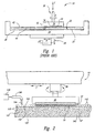
- Figure 1 schematically illustrates a CMP machine 10 with a platen 20, a wafer carrier 30, a polishing pad 40, and a planarization liquid 44 on the polishing pad 40.
- the polishing pad may be a conventional polishing pad made from a non-abrasive material (e.g ., polyurethane), or it may be a new generation fixed-abrasive polishing pad made from abrasive particles fixedly dispersed in a suspension medium.
- the planarization liquid may be a conventional CMP slurry with abrasive particles and chemicals that remove material from the surface of the wafer, or it may be a solution without abrasive particles.
- conventional CMP slurries with abrasive particles are used on conventional polishing pads, and planarizing liquids without abrasive particles are used on fixed-abrasive polishing pads.
- the CMP machine 10 also has an under-pad 25 attached to an upper surface 22 of the platen 20 and the lower surface of the polishing pad 40.
- a drive assembly 26 rotates the platen 20 as indicated by arrow A.
- the drive assembly reciprocates that platen back and forth as indicated by arrow B. Because the polishing pad 40 is attached to the under-pad 25, the polishing pad 40 moves with the platen.
- the wafer carrier 30 has a lower surface 32 to which a wafer 12 may be attached, or the wafer 12 may be attached to a resilient pad 34 positioned between the wafer 12 and the wafer carrier 30.
- the wafer carrier 30 may be a weighted, free-floating wafer carrier or an actuator assembly 36 may be attached to the wafer carrier 30 to impart axial motion, rotational motion, or a combination of axial and rotational motion (indicated by arrows C and D, respectively).
- the wafer carrier 30 presses the wafer 12 face-downward against the polishing pad 40. While the face of the wafer 12 presses against the polishing pad 40, at least one of the platen 20 or the wafer carrier 30 moves relative to the other to move the wafer 12 across the planarizing surface 42. As the face of the wafer 12 moves across the planarizing surface 42, the polishing pad 40 and the planarizing solution 44 continually remove material from the face of the wafer.
- One objective of CMP processing is to produce a uniformly planar surface on the semiconductor wafers.
- the uniformity of the planarized surface is a function of several factors, one of which is the distribution of abrasive particles between the wafer and the polishing pad.
- Fixed-abrasive polishing pads provide a substantially uniform distribution of particles between the wafer and the polishing pad because the abrasive particles are fixedly dispersed in the pad.
- CMP slurries with abrasive particles may not provide a uniform distribution of particles because the slurry builds up at the perimeter of the wafer leaving less slurry under other parts of the wafer. Thus, it is desirable to use fixed-abrasive polishing pads.
- fixed-abrasive polishing pads tend to have a relatively low polishing rate compared to conventional pads and slurries.
- Fixed-abrasive pads are often used without a slurry because conventional planarization slurries with abrasive particles damage the planarizing surface of fixed-abrasive polishing pads.
- the abrasive particles in the slurry generally damage the abrasive particles of the polished pad.
- planarization processes using a polishing pad made from a non-abrasive material in combination with a planarization liquid containing abrasive particles are disclosed in US-A-5,340,370 and WO 96/16436 .
- US-A-5,340,370 teaches polishing of thin films used in integrated circuit manufacturing, e.g. tungsten, tungsten silicide, copper and titanium nitride.
- the planarization liquid contains an abrasive, such as silica, alumina, or ceria, and an oxidant, such as potassium ferricyanide, potassium dichromate, potassium iodate, potassium bromate, and vanadium trioxide.
- the planarization liquid passivates or oxidizes the thin film being polished and then abrasively removes or polishes off the passivated surface.
- WO 96/16436 teaches planarization of silicon semiconductor wafers having tungsten lines and vias.
- the planarization liquid contains abrasives such as alumina, silicon carbide, silicon nitride, silicon dioxide, and ceria. It also contains a ferric salt oxidizer, preferably a ferric salt selected from the group consisting of Fe(NO 3 ) 3 ⁇ 9H 2 O, FeCl 3 ⁇ 6H 2 O, Fe 2 (SO 4 ) 3 ⁇ 5H 2 O and FeNH 4 (SO 4 ) 2 ⁇ 12H 2 O.
- the oxidizer oxidizes the tungsten surface, and then mechanical abrasion of the tungsten oxide by the abrasive particles present in the planarization liquid takes place.
- US-A-3,638,366 discloses a lapping method for metallic workpieces wherein abrasive particles are contained both in the lap itself and in the lapping fluid. Then the working surface is flooded with a non-abrasive cleaning fluid to produce a clean lapped surface.
- the document also mentions a process for lapping metallic workpieces with a bonded abrasive lap, but without loose abrasives. Such processes do not employ any liquid.
- US-A-4,466,218 teaches ultrafinishing magnetic disk substrates with a fixed abrasive polishing pad made from polyurethane foam and hard particles. During polishing a liquid vehicle is supplied in order to remove debris, protect the workpiece and prevent loading or clogging of the workpiece surface. The process also comprises rinse cycles.
- JP-A-6 179 155 teaches polishing with a polishing plate having grooves on the upper surface thereof and having diamond abrasive grains embedded in the surface thereof . During polishing a lubricating fluid is supplied.
- None of the above documents discloses a chemical-mechanical planarization method making use of a combination of an abrasive-free planarizing solution and a fixed-abrasive polishing pad, wherein the material of the surface layer of the substrate to be polished is oxidized and the oxidized material is mechanically removed.
- the inventive CMP process preferably increases the polishing rate and reduces defects in fixed-abrasive pad CMP.
- an abrasive-free planarizing solution is dispensed onto a fixed-abrasive polishing pad.
- the abrasive-free planarizing solution has an oxidant that oxidizes the metal on the surface of the substrate without passing the metal into solution.
- the fixed-abrasive pad has a suspension medium and a substantially uniform distribution of abrasive particles fixedly bonded to the suspension medium.
- the surface layer of the substrate is then pressed against the fixed-abrasive pad in the presence of the planarizing solution, and at least one of the fixed-abrasive pad or the substrate moves relative to the other.
- the planarizing solution forms a rough, scabrous layer of non-soluble oxides on the surface layer that is removed by the abrasive particles of the polishing pad.
- the non-soluble oxides are generally easier to detach from the substrate with mechanical force than the non-oxidized material.
- the planarizing solution has an oxidant, and the pH of the planarizing solution is controlled to oxidize the material of the surface layer without passing it into solution.
- the inventive CMP process may be used to form electrically isolated conductive features on a semiconductor wafer by depositing an upper layer of conductive material onto a top surface of an insulating layer and into depressions in the insulating layer. A portion of the upper conductive layer is removed with the inventive CMP process until the insulating layer is exposed between the depressions in the insulating layer. More specifically, the upper conductive layer is removed by dispensing an abrasive-free, oxidizing planarizing solution onto a fixed-abrasive pad; pressing the upper conductive layer against the fixed-abrasive pad in the presence of the planarizing solution; and moving the upper conductive layer and the fixed-abrasive pad relative to each other. The remaining portions of the upper conductive layer in the depressions of the insulating layer form electrically isolated conductive features.
- the present invention is a method for quickly planarizing a surface layer on a semiconductor wafer with a fixed-abrasive polishing pad.
- An important aspect of the invention is to planarize the surface layer on a fixed-abrasive polishing pad covered with an abrasive-free planarizing solution that oxidizes the material of the surface layer without dissolving the material of the surface layer.
- the thin, oxidized layer on the wafer is readily removed by the abrasive particles in the fixed-abrasive polishing pad, which increases the polishing rate of fixed-abrasive pad CMP.
- the method of the invention therefore, increases the throughput of CMP processes using fixed-abrasive pads.
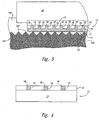
- FIG. 2 is a schematic cross-sectional view of a wafer 12 being planarized on a CMP machine 10 in accordance with a method of the invention.
- the wafer 12 is mounted to a wafer carrier 30 and pressed against a planarizing surface 142 of a fixed-abrasive polishing pad 140 coated with a planarizing solution 144.
- the planarizing solution 144 is preferably dispersed onto the fixed-abrasive polishing pad 140 through a dispenser 146 positioned over the polishing pad and operatively connected to a supply 148 of planarizing solution 144.
- the planarizing solution 144 oxidizes, the material of the surface layer at the front face 14 of the wafer 12 to form a thin layer on the wafer that is easily removed by mechanical force.
- the fixed-abrasive pad 140 has a suspension medium 145 and a plurality of abrasive particles 147 fixedly dispersed in the suspension medium 145.
- the planarizing surface 142 preferably has a number of raised features 143 formed thereon to further abrade the wafer 12.
- the wafer carrier 30 and/or the fixed-abrasive pad 140 move relative to one another while the wafer 12 is pressed against the planarizing surface 142 of the fixed-abrasive pad 140.
- the abrasive particles 147 abrade the thin, oxidized layer (not shown) on the front face 14 of the wafer 12 to remove material from the wafer 12.
- the abrasive particles 147 remove the oxidized surface of the front face 14 of the wafer 12 faster than non-oxidized material.
- the planarizing solution 144 forms an oxide with the material at the surface of the front face 14 of the wafer 12 without dissolving the material.
- the front face 14 of the wafer 12 is a metal that does not oxidize in the presence of air without the assistance of a catalyst, and the planarizing solution is a liquid with an oxidant that causes the particular metal to react with oxygen and form an oxide.
- the specific oxidants in the planarizing solution 144 therefore, depend upon the material of the surface layer at the front face 14 of the wafer 12.
- the material is tungsten, aluminum or copper.
- the planarizing solution has an oxidant in a pH-controlled solution. Accordingly, the particular planarizing solution has a pH that reacts with the material at the front face 14 of the wafer 12 without passing the material into solution.
- the material at the front-face of the wafer may be a single layer of material or a multi-level film stack with several layers of material.
- the planarizing solution 144 forms an oxide with at least some of the layers of a multi-level film stack, and preferably with all of the layers of a multi-level film stack.
- the present invention preferably applies to planarization of single-level and multi-level film formations.
- the present invention is used for planarizing tungsten, aluminum and copper metal layers from the front face 14 of the wafer 12 to form conductive features such as damascene lines and interlayer plugs.
- the planarizing solution preferably has a pH below 5.0 and contains at least one of the following oxidants: hydrogen peroxide and bromine.
- the method of the invention may also be used to planarize aluminum and copper.
- the planarizing solution preferably has a pH of between approximately 3.0 and 10.0, and includes one of the following oxidants: hydrogen peroxide, potassium iodate, or ferric nitrate.
- the planarizing solution preferably has a pH of less than approximately 2.5 or more than approximately 10.5, and has one of the following mixtures: deionized water with 0.1%-5.0% nitric acid and 0.1%-10.0% ethanol; deionized water with 0.1%-5.0% nitric acid and 0.1%-1.0% benzotriazole; deionized water with 0.5%-3.0% ammonium hydroxide; or deionized water with 0.5%-3.0% ammonia ferricyanide.
- Figure 3 illustrates electrically isolated conductive features being formed on the wafer 12 by an embodiment of the method of the invention.
- the wafer 12 generally has a substrate 13, an insulating layer 15 with depressions or vias 16, and an upper conductive layer 17 deposited over the insulating layer 15 and into the vias 16.
- the material of the upper conductive layer 17 fills the vias 16 to form contact plugs 18.
- Several layers of insulating, semi-insulating, semiconducting, and conducting layers may be deposited on the wafer 12 between the substrate 13 and the upper conductive layer 17.
- the wafer 12 is mounted to the wafer carrier 30 and a planarizing solution 144 in accordance with the invention is deposited onto the fixed-abrasive polishing pad 140.
- the planarizing solution does not contain abrasive particles and it oxidizes the material of the upper conductive layer 17 without passing the material of the upper conductive layer 17 into solution.
- the wafer carrier 30 subsequently presses the wafer 12 against the raised features 143 of the fixed-abrasive polishing pad 140. Since the planarizing solution 144 oxidizes the material of the upper conductive layer 17, the planarizing solution 144 forms a thin, scabrous layer 19 across the front face 14 of the wafer 12.
- the scabrous layer 19 has a rough surface with relatively brittle features compared to the surface of non-oxidized material of the upper conductive layer 17.
- the wafer 12 After the wafer 12 is pressed against the fixed-abrasive polishing pad 140, at least one of the wafer 12 or the fixed-abrasive polishing pad 140 moves relative to the other so that the raised features 143 of the fixed-abrasives polishing pad 140 scrape across the scabrous layer 19 of the wafer 12.
- the abrasive particles 147 in the fixed-abrasive polishing pad 140 break the rough, brittle features of the scabrous surface 19 away from the remaining portion of the upper conductive layer 17.
- the planarizing solution 144 continuously oxidizes the newly exposed portions of the upper conductive layer 17 to continuously form a scabrous layer 19 across the surface of the upper conductive layer 17.
- Figure 4 illustrates the wafer 12 after it has been planarized by an embodiment of the chemical-mechanical planarization method of the invention.
- the wafer is planarized until the contiguous portion of the upper conductive layer 17 is removed so that the insulating layer 15 electrically isolates the conductive plugs 18 in the vias 16.
- the planarizing solution 144 is selective to the material of the conductive layer 17 by using chemicals that oxidize the material of the conductive layer 17 without oxidizing or dissolving the material of the insulating layer 15.
- the insulating layer 15 may act as a polish-stop layer to enhance the accuracy of endpointing the CMP process.
- the planarizing solution 144 oxidizes the material of the conductive layer without passing it into solution, the top surface of the contact plugs 18 is substantially flush with the top surface of the insulating layer 15. This is in contrast to slurries and planarizing solutions that dissolve the material of the conductive layer 17. When slurries dissolve the conductive layer 17, they effectively etch the conductive layer 17 and cause the top surface of the contact plugs 18 to be below the top surface of the insulating layer 15. Therefore, unlike CMP methods using planarizing solutions and slurries that etch the material of the conductive layer, the method of the invention generally produces a uniformly planar surface even at the micro level between the contact plugs 18 and the conductive layer 15.
- One advantage of the present invention is that it enhances the throughput of wafers planarized with fixed-abrasive polishing pads without sacrificing the planarity of the wafers.
- the present invention uses an abrasive-free planarizing solution that oxidizes the material of the surface layer without passing it into solution.
- the abrasive particles in the fixed-abrasive polishing pad remove scabrous, oxidized material faster than non-oxidized material.
- the planarizing solution merely oxidizes the material of the surface layer without passing it into solution, the top surface of conductive features are not etched below the top surface of an insulating layer. Therefore, the method of the invention increases throughput and produces highly planar surfaces.
- Another advantage of the present invention is that the fixed-abrasive pad is not damaged by the planarizing solution.
- Conventional slurries with abrasive particles wear down fixed-abrasive pads, and thus they reduce the effectiveness and the useful life of fixed-abrasive pads.
- the planarizing solution used in accordance with the method of the invention does not contain abrasive particles or chemicals that otherwise damage the fixed-abrasive pads.
- the planarizing solution used in accordance with the method of the invention preferably does not damage or otherwise reduce the useful life of fixed-abrasive pads.
- Still another advantage of the present invention is that it reduces the number of defects on wafers planarized with a fixed-abrasive polishing pad. Since conventional slurries with abrasive particles quickly wear down fixed-abrasive polishing pads, many fixed-abrasive pad CMP processes planarize wafers without a solution. However, as discussed above, particles may break away from the fixed-abrasive pads and scratch the surface of the wafer.
- the planarizing solution used in accordance with the method of the invention preferably reduces defects by providing a liquid buffer between a wafer and a fixed-abrasive polishing pad to carry away small particles that may otherwise scratch the surface of the wafer. Therefore, the planarizing solution used in accordance with the method of the invention reduces the number of defects on the surface of the wafer.
- Still another advantage of the present invention is that it enhances the selectivity in planarizing one material with respect to another.
- CMP processes that planarize a wafer on a fixed-abrasive polishing pad without a planarizing solution are not selective to a specific type of material because they do not rely on chemical reactions to remove material from the surface of the wafer.
- the present invention may provide selective planarization because the planarizing solution may be formulated to chemically react with one material differently than another material. Therefore, the present invention preferably enhances the ability to control the removal of a material on specific semiconductor wafer structures.
Landscapes
- Engineering & Computer Science (AREA)
- Physics & Mathematics (AREA)
- Condensed Matter Physics & Semiconductors (AREA)
- General Physics & Mathematics (AREA)
- Manufacturing & Machinery (AREA)
- Computer Hardware Design (AREA)
- Microelectronics & Electronic Packaging (AREA)
- Power Engineering (AREA)
- Mechanical Engineering (AREA)
- Mechanical Treatment Of Semiconductor (AREA)
- Finish Polishing, Edge Sharpening, And Grinding By Specific Grinding Devices (AREA)
- Polishing Bodies And Polishing Tools (AREA)
Claims (16)
- Procédé d'aplanissement chimique/mécanique destiné à éliminer de la matière d'une surface d'un substrat semiconducteur, consistant à :- prévoir une solution d'aplanissement exempte d'abrasif,- prévoir un tampon à abrasif fixe possédant des particules abrasives dispersées dans un milieu de suspension, les particules abrasives fixes étant reliées de manière fixe au milieu de suspension,- placer la solution d'aplanissement sur le tampon à abrasif fixe,- oxyder la matière de la couche de surface du substrat, procédé dans lequel la matière de la couche de surface comprend un métal choisi dans le groupe consistant en du tungstène, de l'aluminium et du cuivre, la solution d'aplanissement comprend un oxydant et forme des oxydes non solubles sur la surface du substrat, et le pH de la solution d'aplanissement est contrôlé afin d'oxyder la matière de la couche de surface sans le faire passer dans la solution, et dans lequel, si le métal est du tungstène, l'oxydant est constitué d'au moins l'un du peroxyde d'hydrogène et du brome, si le métal est de l'aluminium, l'oxydant est constitué d'au moins l'un du peroxyde d'hydrogène, de l'iodate de potassium et du nitrate ferrique, si le métal est du cuivre, la solution d'aplanissement possède un mélange choisi parmi le groupe consistant en un mélange d'eau déminéralisée avec 0,1% à 5,0% d'acide nitrique et 0,1% à 10% d'éthanol, un mélange d'eau déminéralisée avec 0,1% à 5,0% d'acide nitrique et 0,1 à 1,0% de benzotriazole, un mélange d'eau déminéralisée et de 0,5% à 3,0% d'hydroxyde d'ammonium, et un mélange d'eau déminéralisée et de 0,5% à 3,0% de ferricyanure d'ammonium,- éliminer la couche de surface oxydée par les particules abrasives dans le tampon de polissage à abrasif fixe, l'étape d'élimination de la couche de surface oxydée du substrat étant effectuée en pressant la couche de surface contre le patin à abrasif fixe en présence de la solution d'aplanissement, et en déplaçant au moins l'un du tampon à abrasif fixe ou du substrat l'un par rapport à l'autre.
- Procédé selon la revendication 1, dans lequel la surface du substrat comprend du tungstène, et dans lequel l'étape consistant à prévoir la solution d'aplanissement exempte d'abrasif comprend le maintien d'un pH de la solution d'aplanissement au-dessous de 5,0.
- Procédé selon la revendication 2, dans lequel l'étape consistant à prévoir la solution d'aplanissement exempte d'abrasif comprend le maintien du pH de la solution entre 4,0 et 5,0.
- Procédé selon la revendication 2 ou 3, dans lequel la solution d'aplanissement contient du peroxyde d'hydrogène.
- Procédé selon la revendication 2 ou 3, dans lequel la solution d'aplanissement contient du brome.
- Procédé selon la revendication 1, dans lequel la surface du substrat comprend du cuivre, et dans lequel l'étape consistant à prévoir la solution d'aplanissement exempte d'abrasif comprend le maintien d'un pH de la solution inférieur à 2,5 ou supérieur à 10,5.
- Procédé selon la revendication 6, dans lequel la solution d'aplanissement possède un mélange d'eau déminéralisée et de 0,5% à 3,0% d'hydroxyde d'ammonium.
- Procédé selon la revendication 6, dans lequel la solution d'aplanissement possède un mélange d'eau déminéralisée et de 0,5% à 3,0% de ferricyanure d'ammonium.
- Procédé selon la revendication 6, dans lequel la solution d'aplanissement possède un mélange d'eau déminéralisée et de 0,1% à 5,0% d'acide nitrique et de 0,1% à 10,0% d'éthanol.
- Procédé selon la revendication 6, dans lequel la solution d'aplanissement possède un mélange d'eau déminéralisée et de 0,1% à 5,0% d'acide nitrique et de 0,1% à 1,0% de benzotriazole.
- Procédé selon la revendication 1, dans lequel la surface du substrat comprend de l'aluminium, et dans lequel l'étape consistant à prévoir la solution d'aplanissement comprend le maintien d'un pH de la solution entre 3 et 10.
- Procédé selon la revendication 11, dans lequel la solution d'aplanissement contient du peroxyde d'hydrogène.
- Procédé selon la revendication 11, dans lequel la solution d'aplanissement contient de l'iodate de potassium.
- Procédé selon la revendication 11, dans lequel la solution d'aplanissement contient du nitrate ferrique.
- Procédé selon l'une quelconque des revendications 1 à 14, dans lequel des éléments conducteurs électriquement isolés sont formés sur un substrat possédant une couche de matériau conducteur déposée sur une couche d'isolation sur le substrat et dans des creux situés dans la couche d'isolation, en retirant la couche de surface oxydée de la couche conductrice.
- Procédé selon la revendication 15, dans lequel le retrait de la couche de surface oxydée est poursuivi jusqu'à ce que la couche d'isolation soit exposée et isole électriquement le matériau conducteur dans les creux de la couche d'isolation.
Applications Claiming Priority (3)
| Application Number | Priority Date | Filing Date | Title |
|---|---|---|---|
| US732691 | 1985-05-10 | ||
| US08/732,691 US5972792A (en) | 1996-10-18 | 1996-10-18 | Method for chemical-mechanical planarization of a substrate on a fixed-abrasive polishing pad |
| PCT/US1997/019054 WO1998018159A1 (fr) | 1996-10-18 | 1997-10-17 | Procede destine a l'aplanissement chimique-mecanique d'un substrat sur un tampon de polissage a abrasif fixe |
Publications (2)
| Publication Number | Publication Date |
|---|---|
| EP0946979A1 EP0946979A1 (fr) | 1999-10-06 |
| EP0946979B1 true EP0946979B1 (fr) | 2007-09-12 |
Family
ID=24944607
Family Applications (1)
| Application Number | Title | Priority Date | Filing Date |
|---|---|---|---|
| EP97946280A Expired - Lifetime EP0946979B1 (fr) | 1996-10-18 | 1997-10-17 | Procede destine a l'aplanissement chimique-mecanique d'un substrat sur un tampon de polissage a abrasif fixe |
Country Status (8)
| Country | Link |
|---|---|
| US (1) | US5972792A (fr) |
| EP (1) | EP0946979B1 (fr) |
| JP (2) | JP3984296B2 (fr) |
| KR (1) | KR100489458B1 (fr) |
| AT (1) | ATE373317T1 (fr) |
| AU (1) | AU5148198A (fr) |
| DE (1) | DE69738133T2 (fr) |
| WO (1) | WO1998018159A1 (fr) |
Families Citing this family (125)
| Publication number | Priority date | Publication date | Assignee | Title |
|---|---|---|---|---|
| US6258137B1 (en) * | 1992-02-05 | 2001-07-10 | Saint-Gobain Industrial Ceramics, Inc. | CMP products |
| US6075606A (en) | 1996-02-16 | 2000-06-13 | Doan; Trung T. | Endpoint detector and method for measuring a change in wafer thickness in chemical-mechanical polishing of semiconductor wafers and other microelectronic substrates |
| US8092707B2 (en) | 1997-04-30 | 2012-01-10 | 3M Innovative Properties Company | Compositions and methods for modifying a surface suited for semiconductor fabrication |
| US6068879A (en) * | 1997-08-26 | 2000-05-30 | Lsi Logic Corporation | Use of corrosion inhibiting compounds to inhibit corrosion of metal plugs in chemical-mechanical polishing |
| JP3371775B2 (ja) * | 1997-10-31 | 2003-01-27 | 株式会社日立製作所 | 研磨方法 |
| US20040229468A1 (en) * | 1997-10-31 | 2004-11-18 | Seiichi Kondo | Polishing method |
| US6200896B1 (en) | 1998-01-22 | 2001-03-13 | Cypress Semiconductor Corporation | Employing an acidic liquid and an abrasive surface to polish a semiconductor topography |
| US5897426A (en) | 1998-04-24 | 1999-04-27 | Applied Materials, Inc. | Chemical mechanical polishing with multiple polishing pads |
| US6220934B1 (en) | 1998-07-23 | 2001-04-24 | Micron Technology, Inc. | Method for controlling pH during planarization and cleaning of microelectronic substrates |
| JP2000040679A (ja) * | 1998-07-24 | 2000-02-08 | Hitachi Ltd | 半導体集積回路装置の製造方法 |
| JP3858462B2 (ja) * | 1998-07-30 | 2006-12-13 | 株式会社日立製作所 | 半導体装置の製造方法 |
| US5972124A (en) | 1998-08-31 | 1999-10-26 | Advanced Micro Devices, Inc. | Method for cleaning a surface of a dielectric material |
| US6232231B1 (en) * | 1998-08-31 | 2001-05-15 | Cypress Semiconductor Corporation | Planarized semiconductor interconnect topography and method for polishing a metal layer to form interconnect |
| US6566249B1 (en) | 1998-11-09 | 2003-05-20 | Cypress Semiconductor Corp. | Planarized semiconductor interconnect topography and method for polishing a metal layer to form wide interconnect structures |
| US6276996B1 (en) | 1998-11-10 | 2001-08-21 | Micron Technology, Inc. | Copper chemical-mechanical polishing process using a fixed abrasive polishing pad and a copper layer chemical-mechanical polishing solution specifically adapted for chemical-mechanical polishing with a fixed abrasive pad |
| US6206756B1 (en) | 1998-11-10 | 2001-03-27 | Micron Technology, Inc. | Tungsten chemical-mechanical polishing process using a fixed abrasive polishing pad and a tungsten layer chemical-mechanical polishing solution specifically adapted for chemical-mechanical polishing with a fixed abrasive pad |
| AU1804300A (en) * | 1998-12-28 | 2000-07-31 | Hitachi Chemical Company, Ltd. | Materials for polishing liquid for metal, polishing liquid for metal, method forpreparation thereof and polishing method using the same |
| JP2000311876A (ja) * | 1999-04-27 | 2000-11-07 | Hitachi Ltd | 配線基板の製造方法および製造装置 |
| US6419554B2 (en) * | 1999-06-24 | 2002-07-16 | Micron Technology, Inc. | Fixed abrasive chemical-mechanical planarization of titanium nitride |
| US6306012B1 (en) * | 1999-07-20 | 2001-10-23 | Micron Technology, Inc. | Methods and apparatuses for planarizing microelectronic substrate assemblies |
| JP4554011B2 (ja) | 1999-08-10 | 2010-09-29 | ルネサスエレクトロニクス株式会社 | 半導体集積回路装置の製造方法 |
| AU6537000A (en) * | 1999-08-13 | 2001-03-13 | Cabot Microelectronics Corporation | Polishing system with stopping compound and method of its use |
| TW501197B (en) * | 1999-08-17 | 2002-09-01 | Hitachi Chemical Co Ltd | Polishing compound for chemical mechanical polishing and method for polishing substrate |
| US6383934B1 (en) | 1999-09-02 | 2002-05-07 | Micron Technology, Inc. | Method and apparatus for chemical-mechanical planarization of microelectronic substrates with selected planarizing liquids |
| US6306768B1 (en) | 1999-11-17 | 2001-10-23 | Micron Technology, Inc. | Method for planarizing microelectronic substrates having apertures |
| US6379223B1 (en) * | 1999-11-29 | 2002-04-30 | Applied Materials, Inc. | Method and apparatus for electrochemical-mechanical planarization |
| US6358850B1 (en) | 1999-12-23 | 2002-03-19 | International Business Machines Corporation | Slurry-less chemical-mechanical polishing of oxide materials |
| US6294470B1 (en) | 1999-12-22 | 2001-09-25 | International Business Machines Corporation | Slurry-less chemical-mechanical polishing |
| US6498101B1 (en) | 2000-02-28 | 2002-12-24 | Micron Technology, Inc. | Planarizing pads, planarizing machines and methods for making and using planarizing pads in mechanical and chemical-mechanical planarization of microelectronic device substrate assemblies |
| US6313038B1 (en) | 2000-04-26 | 2001-11-06 | Micron Technology, Inc. | Method and apparatus for controlling chemical interactions during planarization of microelectronic substrates |
| JP2003533023A (ja) * | 2000-04-28 | 2003-11-05 | スリーエム イノベイティブ プロパティズ カンパニー | 半導体ウェハの表面を改質する方法 |
| US6387289B1 (en) | 2000-05-04 | 2002-05-14 | Micron Technology, Inc. | Planarizing machines and methods for mechanical and/or chemical-mechanical planarization of microelectronic-device substrate assemblies |
| US6612901B1 (en) | 2000-06-07 | 2003-09-02 | Micron Technology, Inc. | Apparatus for in-situ optical endpointing of web-format planarizing machines in mechanical or chemical-mechanical planarization of microelectronic-device substrate assemblies |
| US6524168B2 (en) | 2000-06-15 | 2003-02-25 | Rodel Holdings, Inc | Composition and method for polishing semiconductors |
| US6646348B1 (en) * | 2000-07-05 | 2003-11-11 | Cabot Microelectronics Corporation | Silane containing polishing composition for CMP |
| US6520834B1 (en) * | 2000-08-09 | 2003-02-18 | Micron Technology, Inc. | Methods and apparatuses for analyzing and controlling performance parameters in mechanical and chemical-mechanical planarization of microelectronic substrates |
| US6602436B2 (en) | 2000-08-11 | 2003-08-05 | Rodel Holdings, Inc | Chemical mechanical planarization of metal substrates |
| US6736869B1 (en) | 2000-08-28 | 2004-05-18 | Micron Technology, Inc. | Method for forming a planarizing pad for planarization of microelectronic substrates |
| US6838382B1 (en) | 2000-08-28 | 2005-01-04 | Micron Technology, Inc. | Method and apparatus for forming a planarizing pad having a film and texture elements for planarization of microelectronic substrates |
| US7160176B2 (en) | 2000-08-30 | 2007-01-09 | Micron Technology, Inc. | Methods and apparatus for electrically and/or chemically-mechanically removing conductive material from a microelectronic substrate |
| US7192335B2 (en) | 2002-08-29 | 2007-03-20 | Micron Technology, Inc. | Method and apparatus for chemically, mechanically, and/or electrolytically removing material from microelectronic substrates |
| US6592443B1 (en) | 2000-08-30 | 2003-07-15 | Micron Technology, Inc. | Method and apparatus for forming and using planarizing pads for mechanical and chemical-mechanical planarization of microelectronic substrates |
| US7134934B2 (en) | 2000-08-30 | 2006-11-14 | Micron Technology, Inc. | Methods and apparatus for electrically detecting characteristics of a microelectronic substrate and/or polishing medium |
| US6602117B1 (en) * | 2000-08-30 | 2003-08-05 | Micron Technology, Inc. | Slurry for use with fixed-abrasive polishing pads in polishing semiconductor device conductive structures that include copper and tungsten and polishing methods |
| US7129160B2 (en) * | 2002-08-29 | 2006-10-31 | Micron Technology, Inc. | Method for simultaneously removing multiple conductive materials from microelectronic substrates |
| US7153410B2 (en) | 2000-08-30 | 2006-12-26 | Micron Technology, Inc. | Methods and apparatus for electrochemical-mechanical processing of microelectronic workpieces |
| US7078308B2 (en) * | 2002-08-29 | 2006-07-18 | Micron Technology, Inc. | Method and apparatus for removing adjacent conductive and nonconductive materials of a microelectronic substrate |
| US7112121B2 (en) | 2000-08-30 | 2006-09-26 | Micron Technology, Inc. | Methods and apparatus for electrical, mechanical and/or chemical removal of conductive material from a microelectronic substrate |
| US7220166B2 (en) * | 2000-08-30 | 2007-05-22 | Micron Technology, Inc. | Methods and apparatus for electromechanically and/or electrochemically-mechanically removing conductive material from a microelectronic substrate |
| US6609947B1 (en) | 2000-08-30 | 2003-08-26 | Micron Technology, Inc. | Planarizing machines and control systems for mechanical and/or chemical-mechanical planarization of micro electronic substrates |
| US7074113B1 (en) | 2000-08-30 | 2006-07-11 | Micron Technology, Inc. | Methods and apparatus for removing conductive material from a microelectronic substrate |
| US7094131B2 (en) | 2000-08-30 | 2006-08-22 | Micron Technology, Inc. | Microelectronic substrate having conductive material with blunt cornered apertures, and associated methods for removing conductive material |
| US6551935B1 (en) * | 2000-08-31 | 2003-04-22 | Micron Technology, Inc. | Slurry for use in polishing semiconductor device conductive structures that include copper and tungsten and polishing methods |
| US7153195B2 (en) * | 2000-08-30 | 2006-12-26 | Micron Technology, Inc. | Methods and apparatus for selectively removing conductive material from a microelectronic substrate |
| US6867448B1 (en) | 2000-08-31 | 2005-03-15 | Micron Technology, Inc. | Electro-mechanically polished structure |
| US6623329B1 (en) | 2000-08-31 | 2003-09-23 | Micron Technology, Inc. | Method and apparatus for supporting a microelectronic substrate relative to a planarization pad |
| US6652764B1 (en) | 2000-08-31 | 2003-11-25 | Micron Technology, Inc. | Methods and apparatuses for making and using planarizing pads for mechanical and chemical-mechanical planarization of microelectronic substrates |
| US6468137B1 (en) * | 2000-09-07 | 2002-10-22 | Cabot Microelectronics Corporation | Method for polishing a memory or rigid disk with an oxidized halide-containing polishing system |
| US6328042B1 (en) | 2000-10-05 | 2001-12-11 | Lam Research Corporation | Wafer cleaning module and method for cleaning the surface of a substrate |
| US20020098784A1 (en) * | 2001-01-19 | 2002-07-25 | Saket Chadda | Abrasive free polishing in copper damascene applications |
| PL363342A1 (en) * | 2001-02-08 | 2004-11-15 | Rem Technologies, Inc. | Chemical mechanical machining and surface finishing |
| US6849547B2 (en) * | 2001-04-05 | 2005-02-01 | Speedfam Ipec Corporation | Apparatus and process for polishing a workpiece |
| JP2002324772A (ja) | 2001-04-25 | 2002-11-08 | Hitachi Ltd | 半導体装置の製造方法及び製造装置 |
| US6969684B1 (en) | 2001-04-30 | 2005-11-29 | Cypress Semiconductor Corp. | Method of making a planarized semiconductor structure |
| US6485355B1 (en) | 2001-06-22 | 2002-11-26 | International Business Machines Corporation | Method to increase removal rate of oxide using fixed-abrasive |
| US6800218B2 (en) | 2001-08-23 | 2004-10-05 | Advanced Technology Materials, Inc. | Abrasive free formulations for chemical mechanical polishing of copper and associated materials and method of using same |
| US6722943B2 (en) | 2001-08-24 | 2004-04-20 | Micron Technology, Inc. | Planarizing machines and methods for dispensing planarizing solutions in the processing of microelectronic workpieces |
| US6866566B2 (en) | 2001-08-24 | 2005-03-15 | Micron Technology, Inc. | Apparatus and method for conditioning a contact surface of a processing pad used in processing microelectronic workpieces |
| US6784018B2 (en) * | 2001-08-29 | 2004-08-31 | Micron Technology, Inc. | Method of forming chalcogenide comprising devices and method of forming a programmable memory cell of memory circuitry |
| US6666749B2 (en) | 2001-08-30 | 2003-12-23 | Micron Technology, Inc. | Apparatus and method for enhanced processing of microelectronic workpieces |
| US6659846B2 (en) | 2001-09-17 | 2003-12-09 | Agere Systems, Inc. | Pad for chemical mechanical polishing |
| US6702866B2 (en) | 2002-01-10 | 2004-03-09 | Speedfam-Ipec Corporation | Homogeneous fixed abrasive polishing pad |
| US6841480B2 (en) * | 2002-02-04 | 2005-01-11 | Infineon Technologies Ag | Polyelectrolyte dispensing polishing pad, production thereof and method of polishing a substrate |
| JPWO2003071593A1 (ja) * | 2002-02-20 | 2005-06-16 | 株式会社荏原製作所 | ポリッシング方法および研磨液 |
| US7131889B1 (en) | 2002-03-04 | 2006-11-07 | Micron Technology, Inc. | Method for planarizing microelectronic workpieces |
| US6828678B1 (en) | 2002-03-29 | 2004-12-07 | Silicon Magnetic Systems | Semiconductor topography with a fill material arranged within a plurality of valleys associated with the surface roughness of the metal layer |
| US6869335B2 (en) | 2002-07-08 | 2005-03-22 | Micron Technology, Inc. | Retaining rings, planarizing apparatuses including retaining rings, and methods for planarizing micro-device workpieces |
| US7341502B2 (en) | 2002-07-18 | 2008-03-11 | Micron Technology, Inc. | Methods and systems for planarizing workpieces, e.g., microelectronic workpieces |
| US6860798B2 (en) | 2002-08-08 | 2005-03-01 | Micron Technology, Inc. | Carrier assemblies, planarizing apparatuses including carrier assemblies, and methods for planarizing micro-device workpieces |
| US7094695B2 (en) | 2002-08-21 | 2006-08-22 | Micron Technology, Inc. | Apparatus and method for conditioning a polishing pad used for mechanical and/or chemical-mechanical planarization |
| US7004817B2 (en) | 2002-08-23 | 2006-02-28 | Micron Technology, Inc. | Carrier assemblies, planarizing apparatuses including carrier assemblies, and methods for planarizing micro-device workpieces |
| US7011566B2 (en) | 2002-08-26 | 2006-03-14 | Micron Technology, Inc. | Methods and systems for conditioning planarizing pads used in planarizing substrates |
| US7235488B2 (en) * | 2002-08-28 | 2007-06-26 | Micron Technology, Inc. | In-situ chemical-mechanical planarization pad metrology using ultrasonic imaging |
| US7008299B2 (en) | 2002-08-29 | 2006-03-07 | Micron Technology, Inc. | Apparatus and method for mechanical and/or chemical-mechanical planarization of micro-device workpieces |
| US6841991B2 (en) | 2002-08-29 | 2005-01-11 | Micron Technology, Inc. | Planarity diagnostic system, E.G., for microelectronic component test systems |
| US7074114B2 (en) | 2003-01-16 | 2006-07-11 | Micron Technology, Inc. | Carrier assemblies, polishing machines including carrier assemblies, and methods for polishing micro-device workpieces |
| US6899597B2 (en) * | 2003-01-29 | 2005-05-31 | Infineon Technologies Ag | Chemical mechanical polishing (CMP) process using fixed abrasive pads |
| US6884152B2 (en) * | 2003-02-11 | 2005-04-26 | Micron Technology, Inc. | Apparatuses and methods for conditioning polishing pads used in polishing micro-device workpieces |
| US7066801B2 (en) | 2003-02-21 | 2006-06-27 | Dow Global Technologies, Inc. | Method of manufacturing a fixed abrasive material |
| US6910951B2 (en) | 2003-02-24 | 2005-06-28 | Dow Global Technologies, Inc. | Materials and methods for chemical-mechanical planarization |
| US6872132B2 (en) | 2003-03-03 | 2005-03-29 | Micron Technology, Inc. | Systems and methods for monitoring characteristics of a polishing pad used in polishing micro-device workpieces |
| US7131891B2 (en) | 2003-04-28 | 2006-11-07 | Micron Technology, Inc. | Systems and methods for mechanical and/or chemical-mechanical polishing of microfeature workpieces |
| US6935929B2 (en) | 2003-04-28 | 2005-08-30 | Micron Technology, Inc. | Polishing machines including under-pads and methods for mechanical and/or chemical-mechanical polishing of microfeature workpieces |
| US7030603B2 (en) | 2003-08-21 | 2006-04-18 | Micron Technology, Inc. | Apparatuses and methods for monitoring rotation of a conductive microfeature workpiece |
| US7112122B2 (en) * | 2003-09-17 | 2006-09-26 | Micron Technology, Inc. | Methods and apparatus for removing conductive material from a microelectronic substrate |
| US7153777B2 (en) | 2004-02-20 | 2006-12-26 | Micron Technology, Inc. | Methods and apparatuses for electrochemical-mechanical polishing |
| US7086927B2 (en) | 2004-03-09 | 2006-08-08 | Micron Technology, Inc. | Methods and systems for planarizing workpieces, e.g., microelectronic workpieces |
| US7195544B2 (en) * | 2004-03-23 | 2007-03-27 | Cabot Microelectronics Corporation | CMP porous pad with component-filled pores |
| US7514016B2 (en) * | 2004-07-30 | 2009-04-07 | Hitachi Global Storage Technologies Netherlands, Bv | Methodology of chemical mechanical nanogrinding for ultra precision finishing of workpieces |
| US7066792B2 (en) | 2004-08-06 | 2006-06-27 | Micron Technology, Inc. | Shaped polishing pads for beveling microfeature workpiece edges, and associate system and methods |
| JP4725767B2 (ja) * | 2004-08-12 | 2011-07-13 | 有限会社岡本光学加工所 | 光学材料の無歪み表面加工装置および表面加工技術 |
| US7033253B2 (en) | 2004-08-12 | 2006-04-25 | Micron Technology, Inc. | Polishing pad conditioners having abrasives and brush elements, and associated systems and methods |
| US7566391B2 (en) | 2004-09-01 | 2009-07-28 | Micron Technology, Inc. | Methods and systems for removing materials from microfeature workpieces with organic and/or non-aqueous electrolytic media |
| US7264539B2 (en) | 2005-07-13 | 2007-09-04 | Micron Technology, Inc. | Systems and methods for removing microfeature workpiece surface defects |
| US7438626B2 (en) | 2005-08-31 | 2008-10-21 | Micron Technology, Inc. | Apparatus and method for removing material from microfeature workpieces |
| US7326105B2 (en) | 2005-08-31 | 2008-02-05 | Micron Technology, Inc. | Retaining rings, and associated planarizing apparatuses, and related methods for planarizing micro-device workpieces |
| US7294049B2 (en) | 2005-09-01 | 2007-11-13 | Micron Technology, Inc. | Method and apparatus for removing material from microfeature workpieces |
| US7201634B1 (en) * | 2005-11-14 | 2007-04-10 | Infineon Technologies Ag | Polishing methods and apparatus |
| US7849281B2 (en) * | 2006-04-03 | 2010-12-07 | Emc Corporation | Method and system for implementing hierarchical permission maps in a layered volume graph |
| JP5151133B2 (ja) * | 2006-12-11 | 2013-02-27 | 富士通株式会社 | 配線形成方法 |
| US7754612B2 (en) | 2007-03-14 | 2010-07-13 | Micron Technology, Inc. | Methods and apparatuses for removing polysilicon from semiconductor workpieces |
| JP4618267B2 (ja) * | 2007-04-12 | 2011-01-26 | 株式会社日立製作所 | 半導体装置の製造方法 |
| KR20090002506A (ko) * | 2007-06-29 | 2009-01-09 | 제일모직주식회사 | 상변화 메모리 소자 연마용 cmp 슬러리 조성물 및 이를이용한 연마 방법 |
| US7678605B2 (en) * | 2007-08-30 | 2010-03-16 | Dupont Air Products Nanomaterials Llc | Method for chemical mechanical planarization of chalcogenide materials |
| US7915071B2 (en) * | 2007-08-30 | 2011-03-29 | Dupont Air Products Nanomaterials, Llc | Method for chemical mechanical planarization of chalcogenide materials |
| KR20090127707A (ko) * | 2008-06-09 | 2009-12-14 | 삼성전자주식회사 | 화학 기계적 연마 공정을 이용한 반도체 소자의 트랜치소자 분리 방법 |
| EP2192609A1 (fr) * | 2008-11-28 | 2010-06-02 | SUMCO Corporation | Procédé de fabrication d'une tranche pour une couche active |
| JP5343250B2 (ja) * | 2009-02-19 | 2013-11-13 | 国立大学法人 熊本大学 | 触媒支援型化学加工方法及びそれを用いた加工装置 |
| US8500515B2 (en) * | 2010-03-12 | 2013-08-06 | Wayne O. Duescher | Fixed-spindle and floating-platen abrasive system using spherical mounts |
| US8740668B2 (en) * | 2010-03-12 | 2014-06-03 | Wayne O. Duescher | Three-point spindle-supported floating abrasive platen |
| US8647171B2 (en) * | 2010-03-12 | 2014-02-11 | Wayne O. Duescher | Fixed-spindle floating-platen workpiece loader apparatus |
| US8602842B2 (en) * | 2010-03-12 | 2013-12-10 | Wayne O. Duescher | Three-point fixed-spindle floating-platen abrasive system |
| US20110275216A1 (en) * | 2010-05-04 | 2011-11-10 | Macronix International Co., Ltd. | Two step chemical-mechanical polishing process |
| DE102010042040A1 (de) | 2010-10-06 | 2012-04-12 | Siltronic Ag | Verfahren zum Schleifen einer Halbleiterscheibe |
| US20140364041A1 (en) * | 2011-12-16 | 2014-12-11 | Lg Siltron Inc. | Apparatus and method for polishing wafer |
Family Cites Families (32)
| Publication number | Priority date | Publication date | Assignee | Title |
|---|---|---|---|---|
| US3638366A (en) * | 1969-12-03 | 1972-02-01 | Norton Co | Lapping method for metallic workpieces |
| US3957553A (en) * | 1972-08-09 | 1976-05-18 | Pennwalt Corporation | Non-chromated alkaline etching bath and etching process for aluminum |
| US4927432A (en) * | 1986-03-25 | 1990-05-22 | Rodel, Inc. | Pad material for grinding, lapping and polishing |
| JPH01193166A (ja) * | 1988-01-28 | 1989-08-03 | Showa Denko Kk | 半導体ウェハ鏡面研磨用パッド |
| US4879258A (en) * | 1988-08-31 | 1989-11-07 | Texas Instruments Incorporated | Integrated circuit planarization by mechanical polishing |
| US4910155A (en) * | 1988-10-28 | 1990-03-20 | International Business Machines Corporation | Wafer flood polishing |
| US4903440A (en) * | 1988-11-23 | 1990-02-27 | Minnesota Mining And Manufacturing Company | Abrasive product having binder comprising an aminoplast resin |
| US4954142A (en) * | 1989-03-07 | 1990-09-04 | International Business Machines Corporation | Method of chemical-mechanical polishing an electronic component substrate and polishing slurry therefor |
| US4992135A (en) * | 1990-07-24 | 1991-02-12 | Micron Technology, Inc. | Method of etching back of tungsten layers on semiconductor wafers, and solution therefore |
| JPH05177523A (ja) * | 1991-06-06 | 1993-07-20 | Commiss Energ Atom | 張設された微小研磨剤小板、および改良されたウエハー支持ヘッドを備えた研磨装置 |
| US5262354A (en) * | 1992-02-26 | 1993-11-16 | International Business Machines Corporation | Refractory metal capped low resistivity metal conductor lines and vias |
| US5209816A (en) * | 1992-06-04 | 1993-05-11 | Micron Technology, Inc. | Method of chemical mechanical polishing aluminum containing metal layers and slurry for chemical mechanical polishing |
| US5225034A (en) * | 1992-06-04 | 1993-07-06 | Micron Technology, Inc. | Method of chemical mechanical polishing predominantly copper containing metal layers in semiconductor processing |
| MY114512A (en) * | 1992-08-19 | 2002-11-30 | Rodel Inc | Polymeric substrate with polymeric microelements |
| US5300155A (en) * | 1992-12-23 | 1994-04-05 | Micron Semiconductor, Inc. | IC chemical mechanical planarization process incorporating slurry temperature control |
| US5482497A (en) * | 1992-12-30 | 1996-01-09 | International Business Machines Corporation | Method and apparatus for texturing zones of a magnetic disk |
| US5392950A (en) * | 1993-04-20 | 1995-02-28 | Continental Plastic Containers, Inc. | Plastic container with a completely sealed handle |
| US5318927A (en) * | 1993-04-29 | 1994-06-07 | Micron Semiconductor, Inc. | Methods of chemical-mechanical polishing insulating inorganic metal oxide materials |
| US5391258A (en) * | 1993-05-26 | 1995-02-21 | Rodel, Inc. | Compositions and methods for polishing |
| US5453312A (en) * | 1993-10-29 | 1995-09-26 | Minnesota Mining And Manufacturing Company | Abrasive article, a process for its manufacture, and a method of using it to reduce a workpiece surface |
| US5340370A (en) * | 1993-11-03 | 1994-08-23 | Intel Corporation | Slurries for chemical mechanical polishing |
| US5575885A (en) * | 1993-12-14 | 1996-11-19 | Kabushiki Kaisha Toshiba | Copper-based metal polishing solution and method for manufacturing semiconductor device |
| JP2894209B2 (ja) * | 1994-06-03 | 1999-05-24 | 信越半導体株式会社 | シリコンウェーハ研磨用パッド及び研磨方法 |
| JPH0864562A (ja) * | 1994-08-24 | 1996-03-08 | Matsushita Electric Ind Co Ltd | 半導体研磨方法及び装置 |
| US5527423A (en) * | 1994-10-06 | 1996-06-18 | Cabot Corporation | Chemical mechanical polishing slurry for metal layers |
| JPH08112740A (ja) * | 1994-10-13 | 1996-05-07 | Olympus Optical Co Ltd | 窒化アルミニウムの研磨方法 |
| US5643044A (en) * | 1994-11-01 | 1997-07-01 | Lund; Douglas E. | Automatic chemical and mechanical polishing system for semiconductor wafers |
| EP0792515A1 (fr) * | 1994-11-18 | 1997-09-03 | Advanced Micro Devices, Inc. | Procede de fabrication d'une suspension chimio-mecanique destinee au polissage et la suspension elle-meme |
| US5534462A (en) * | 1995-02-24 | 1996-07-09 | Motorola, Inc. | Method for forming a plug and semiconductor device having the same |
| US5707492A (en) * | 1995-12-18 | 1998-01-13 | Motorola, Inc. | Metallized pad polishing process |
| US5624303A (en) * | 1996-01-22 | 1997-04-29 | Micron Technology, Inc. | Polishing pad and a method for making a polishing pad with covalently bonded particles |
| US5759427A (en) * | 1996-08-28 | 1998-06-02 | International Business Machines Corporation | Method and apparatus for polishing metal surfaces |
-
1996
- 1996-10-18 US US08/732,691 patent/US5972792A/en not_active Expired - Lifetime
-
1997
- 1997-10-17 JP JP51958998A patent/JP3984296B2/ja not_active Expired - Fee Related
- 1997-10-17 WO PCT/US1997/019054 patent/WO1998018159A1/fr not_active Ceased
- 1997-10-17 AU AU51481/98A patent/AU5148198A/en not_active Abandoned
- 1997-10-17 AT AT97946280T patent/ATE373317T1/de not_active IP Right Cessation
- 1997-10-17 DE DE69738133T patent/DE69738133T2/de not_active Expired - Lifetime
- 1997-10-17 EP EP97946280A patent/EP0946979B1/fr not_active Expired - Lifetime
- 1997-10-17 KR KR10-1999-7003413A patent/KR100489458B1/ko not_active Expired - Lifetime
-
2006
- 2006-02-28 JP JP2006054151A patent/JP2006148174A/ja active Pending
Also Published As
| Publication number | Publication date |
|---|---|
| EP0946979A1 (fr) | 1999-10-06 |
| JP2006148174A (ja) | 2006-06-08 |
| JP2001502610A (ja) | 2001-02-27 |
| US5972792A (en) | 1999-10-26 |
| AU5148198A (en) | 1998-05-15 |
| ATE373317T1 (de) | 2007-09-15 |
| KR100489458B1 (ko) | 2005-05-16 |
| KR20000052645A (ko) | 2000-08-25 |
| DE69738133D1 (de) | 2007-10-25 |
| DE69738133T2 (de) | 2008-06-12 |
| WO1998018159A1 (fr) | 1998-04-30 |
| JP3984296B2 (ja) | 2007-10-03 |
Similar Documents
| Publication | Publication Date | Title |
|---|---|---|
| EP0946979B1 (fr) | Procede destine a l'aplanissement chimique-mecanique d'un substrat sur un tampon de polissage a abrasif fixe | |
| US7104869B2 (en) | Barrier removal at low polish pressure | |
| US6039633A (en) | Method and apparatus for mechanical and chemical-mechanical planarization of microelectronic-device substrate assemblies | |
| US6589101B2 (en) | Method and apparatus for mechanical and chemical-mechanical planarization of microelectronic substrates with metal compound abrasives | |
| US6254460B1 (en) | Fixed abrasive polishing pad | |
| US6368190B1 (en) | Electrochemical mechanical planarization apparatus and method | |
| JP4095731B2 (ja) | 半導体装置の製造方法及び半導体装置 | |
| US5755979A (en) | Application of semiconductor IC fabrication techniques to the manufacturing of a conditioning head for pad conditioning during chemical-mechanical polish | |
| US6783432B2 (en) | Additives for pressure sensitive polishing compositions | |
| US20050189235A1 (en) | Multi-phase polishing pad | |
| KR20000058021A (ko) | 화학적 기계적 연마 처리 및 부품 | |
| US7012025B2 (en) | Tantalum removal during chemical mechanical polishing | |
| US6677239B2 (en) | Methods and compositions for chemical mechanical polishing | |
| US20020173221A1 (en) | Method and apparatus for two-step polishing | |
| US7244168B2 (en) | Methods for reducing delamination during chemical mechanical polishing | |
| WO2008058200A2 (fr) | Procédés et appareils destinés au polissage électrochimico-mécanique de substrats nip | |
| JP4756814B2 (ja) | ルテニウムcmp用溶液及びこれらを利用するルテニウムパターン形成方法 | |
| US6599837B1 (en) | Chemical mechanical polishing composition and method of polishing metal layers using same | |
| JP2004128112A (ja) | 半導体装置の製造方法 | |
| Jin et al. | Advanced front end CMP and integration solutions | |
| JP2005260185A (ja) | 研磨パッド | |
| WO2005058543A1 (fr) | Methode s'appliquant a un processus de planarisation electro-chimio-mecanique |
Legal Events
| Date | Code | Title | Description |
|---|---|---|---|
| PUAI | Public reference made under article 153(3) epc to a published international application that has entered the european phase |
Free format text: ORIGINAL CODE: 0009012 |
|
| 17P | Request for examination filed |
Effective date: 19990512 |
|
| AK | Designated contracting states |
Kind code of ref document: A1 Designated state(s): AT BE CH DE DK ES FI FR GB GR IE IT LI LU MC NL PT SE |
|
| RIN1 | Information on inventor provided before grant (corrected) |
Inventor name: HUDSON, GUY, F. |
|
| 17Q | First examination report despatched |
Effective date: 20010517 |
|
| APBR | Date of receipt of statement of grounds of appeal recorded |
Free format text: ORIGINAL CODE: EPIDOSNNOA3E |
|
| APAZ | Date of receipt of statement of grounds of appeal deleted |
Free format text: ORIGINAL CODE: EPIDOSDNOA3E |
|
| APBR | Date of receipt of statement of grounds of appeal recorded |
Free format text: ORIGINAL CODE: EPIDOSNNOA3E |
|
| APAF | Appeal reference modified |
Free format text: ORIGINAL CODE: EPIDOSCREFNE |
|
| APBT | Appeal procedure closed |
Free format text: ORIGINAL CODE: EPIDOSNNOA9E |
|
| APBV | Interlocutory revision of appeal recorded |
Free format text: ORIGINAL CODE: EPIDOSNIRAPE |
|
| GRAP | Despatch of communication of intention to grant a patent |
Free format text: ORIGINAL CODE: EPIDOSNIGR1 |
|
| GRAS | Grant fee paid |
Free format text: ORIGINAL CODE: EPIDOSNIGR3 |
|
| GRAA | (expected) grant |
Free format text: ORIGINAL CODE: 0009210 |
|
| AK | Designated contracting states |
Kind code of ref document: B1 Designated state(s): AT BE CH DE DK ES FI FR GB GR IE IT LI LU MC NL PT SE |
|
| REG | Reference to a national code |
Ref country code: GB Ref legal event code: FG4D |
|
| REG | Reference to a national code |
Ref country code: CH Ref legal event code: EP |
|
| REF | Corresponds to: |
Ref document number: 69738133 Country of ref document: DE Date of ref document: 20071025 Kind code of ref document: P |
|
| REG | Reference to a national code |
Ref country code: IE Ref legal event code: FG4D |
|
| ET | Fr: translation filed | ||
| PG25 | Lapsed in a contracting state [announced via postgrant information from national office to epo] |
Ref country code: FI Free format text: LAPSE BECAUSE OF FAILURE TO SUBMIT A TRANSLATION OF THE DESCRIPTION OR TO PAY THE FEE WITHIN THE PRESCRIBED TIME-LIMIT Effective date: 20070912 |
|
| PG25 | Lapsed in a contracting state [announced via postgrant information from national office to epo] |
Ref country code: AT Free format text: LAPSE BECAUSE OF FAILURE TO SUBMIT A TRANSLATION OF THE DESCRIPTION OR TO PAY THE FEE WITHIN THE PRESCRIBED TIME-LIMIT Effective date: 20070912 Ref country code: LI Free format text: LAPSE BECAUSE OF FAILURE TO SUBMIT A TRANSLATION OF THE DESCRIPTION OR TO PAY THE FEE WITHIN THE PRESCRIBED TIME-LIMIT Effective date: 20070912 Ref country code: CH Free format text: LAPSE BECAUSE OF FAILURE TO SUBMIT A TRANSLATION OF THE DESCRIPTION OR TO PAY THE FEE WITHIN THE PRESCRIBED TIME-LIMIT Effective date: 20070912 |
|
| NLV1 | Nl: lapsed or annulled due to failure to fulfill the requirements of art. 29p and 29m of the patents act | ||
| PG25 | Lapsed in a contracting state [announced via postgrant information from national office to epo] |
Ref country code: BE Free format text: LAPSE BECAUSE OF FAILURE TO SUBMIT A TRANSLATION OF THE DESCRIPTION OR TO PAY THE FEE WITHIN THE PRESCRIBED TIME-LIMIT Effective date: 20070912 |
|
| REG | Reference to a national code |
Ref country code: CH Ref legal event code: PL |
|
| PG25 | Lapsed in a contracting state [announced via postgrant information from national office to epo] |
Ref country code: NL Free format text: LAPSE BECAUSE OF FAILURE TO SUBMIT A TRANSLATION OF THE DESCRIPTION OR TO PAY THE FEE WITHIN THE PRESCRIBED TIME-LIMIT Effective date: 20070912 Ref country code: GR Free format text: LAPSE BECAUSE OF FAILURE TO SUBMIT A TRANSLATION OF THE DESCRIPTION OR TO PAY THE FEE WITHIN THE PRESCRIBED TIME-LIMIT Effective date: 20071213 Ref country code: ES Free format text: LAPSE BECAUSE OF FAILURE TO SUBMIT A TRANSLATION OF THE DESCRIPTION OR TO PAY THE FEE WITHIN THE PRESCRIBED TIME-LIMIT Effective date: 20071223 |
|
| PG25 | Lapsed in a contracting state [announced via postgrant information from national office to epo] |
Ref country code: PT Free format text: LAPSE BECAUSE OF FAILURE TO SUBMIT A TRANSLATION OF THE DESCRIPTION OR TO PAY THE FEE WITHIN THE PRESCRIBED TIME-LIMIT Effective date: 20080212 Ref country code: MC Free format text: LAPSE BECAUSE OF NON-PAYMENT OF DUE FEES Effective date: 20071031 |
|
| PG25 | Lapsed in a contracting state [announced via postgrant information from national office to epo] |
Ref country code: SE Free format text: LAPSE BECAUSE OF FAILURE TO SUBMIT A TRANSLATION OF THE DESCRIPTION OR TO PAY THE FEE WITHIN THE PRESCRIBED TIME-LIMIT Effective date: 20071212 |
|
| PLBE | No opposition filed within time limit |
Free format text: ORIGINAL CODE: 0009261 |
|
| STAA | Information on the status of an ep patent application or granted ep patent |
Free format text: STATUS: NO OPPOSITION FILED WITHIN TIME LIMIT |
|
| PG25 | Lapsed in a contracting state [announced via postgrant information from national office to epo] |
Ref country code: DK Free format text: LAPSE BECAUSE OF FAILURE TO SUBMIT A TRANSLATION OF THE DESCRIPTION OR TO PAY THE FEE WITHIN THE PRESCRIBED TIME-LIMIT Effective date: 20070912 |
|
| 26N | No opposition filed |
Effective date: 20080613 |
|
| PG25 | Lapsed in a contracting state [announced via postgrant information from national office to epo] |
Ref country code: IE Free format text: LAPSE BECAUSE OF NON-PAYMENT OF DUE FEES Effective date: 20071017 |
|
| PG25 | Lapsed in a contracting state [announced via postgrant information from national office to epo] |
Ref country code: LU Free format text: LAPSE BECAUSE OF NON-PAYMENT OF DUE FEES Effective date: 20071017 |
|
| PGFP | Annual fee paid to national office [announced via postgrant information from national office to epo] |
Ref country code: DE Payment date: 20141014 Year of fee payment: 18 Ref country code: FR Payment date: 20141008 Year of fee payment: 18 |
|
| PGFP | Annual fee paid to national office [announced via postgrant information from national office to epo] |
Ref country code: IT Payment date: 20141024 Year of fee payment: 18 |
|
| PGFP | Annual fee paid to national office [announced via postgrant information from national office to epo] |
Ref country code: GB Payment date: 20150107 Year of fee payment: 18 |
|
| REG | Reference to a national code |
Ref country code: DE Ref legal event code: R119 Ref document number: 69738133 Country of ref document: DE |
|
| GBPC | Gb: european patent ceased through non-payment of renewal fee |
Effective date: 20151017 |
|
| PG25 | Lapsed in a contracting state [announced via postgrant information from national office to epo] |
Ref country code: GB Free format text: LAPSE BECAUSE OF NON-PAYMENT OF DUE FEES Effective date: 20151017 Ref country code: DE Free format text: LAPSE BECAUSE OF NON-PAYMENT OF DUE FEES Effective date: 20160503 Ref country code: IT Free format text: LAPSE BECAUSE OF NON-PAYMENT OF DUE FEES Effective date: 20151017 |
|
| REG | Reference to a national code |
Ref country code: FR Ref legal event code: ST Effective date: 20160630 |
|
| PG25 | Lapsed in a contracting state [announced via postgrant information from national office to epo] |
Ref country code: FR Free format text: LAPSE BECAUSE OF NON-PAYMENT OF DUE FEES Effective date: 20151102 |