EP0944243B1 - Color image forming apparatus and scanning optical apparatus - Google Patents
Color image forming apparatus and scanning optical apparatus Download PDFInfo
- Publication number
- EP0944243B1 EP0944243B1 EP99105248.1A EP99105248A EP0944243B1 EP 0944243 B1 EP0944243 B1 EP 0944243B1 EP 99105248 A EP99105248 A EP 99105248A EP 0944243 B1 EP0944243 B1 EP 0944243B1
- Authority
- EP
- European Patent Office
- Prior art keywords
- scanning
- optical element
- diffracting
- optical
- optical device
- Prior art date
- Legal status (The legal status is an assumption and is not a legal conclusion. Google has not performed a legal analysis and makes no representation as to the accuracy of the status listed.)
- Expired - Lifetime
Links
- 230000003287 optical effect Effects 0.000 title claims description 212
- 238000003384 imaging method Methods 0.000 claims description 6
- 238000006073 displacement reaction Methods 0.000 claims description 2
- 238000010586 diagram Methods 0.000 description 25
- 239000003086 colorant Substances 0.000 description 15
- 238000001514 detection method Methods 0.000 description 14
- 239000010410 layer Substances 0.000 description 11
- 230000000694 effects Effects 0.000 description 8
- 239000002184 metal Substances 0.000 description 7
- 230000006870 function Effects 0.000 description 6
- 238000000034 method Methods 0.000 description 6
- 239000000463 material Substances 0.000 description 5
- 230000007246 mechanism Effects 0.000 description 5
- 239000011347 resin Substances 0.000 description 5
- 229920005989 resin Polymers 0.000 description 5
- 239000000758 substrate Substances 0.000 description 5
- 230000008859 change Effects 0.000 description 2
- 230000001105 regulatory effect Effects 0.000 description 2
- 239000004065 semiconductor Substances 0.000 description 2
- 230000005540 biological transmission Effects 0.000 description 1
- 230000015572 biosynthetic process Effects 0.000 description 1
- 238000011161 development Methods 0.000 description 1
- 230000018109 developmental process Effects 0.000 description 1
- 239000011521 glass Substances 0.000 description 1
- 238000001746 injection moulding Methods 0.000 description 1
- 230000015654 memory Effects 0.000 description 1
- 230000008569 process Effects 0.000 description 1
- 239000002356 single layer Substances 0.000 description 1
- 230000001360 synchronised effect Effects 0.000 description 1
Images


Classifications
-
- H—ELECTRICITY
- H04—ELECTRIC COMMUNICATION TECHNIQUE
- H04N—PICTORIAL COMMUNICATION, e.g. TELEVISION
- H04N1/00—Scanning, transmission or reproduction of documents or the like, e.g. facsimile transmission; Details thereof
- H04N1/46—Colour picture communication systems
- H04N1/50—Picture reproducers
- H04N1/506—Reproducing the colour component signals picture-sequentially, e.g. with reproducing heads spaced apart from one another in the subscanning direction
Definitions
- the present invention relates to a color image forming apparatus and a scanning optical apparatus and, more particularly, to those arranged to record color image information or the like with suppressing scanning line deviation among colors and with suppressing asymmetric magnification (component of slope of magnification) (image height deviation), for example, such as those suitably applicable to such apparatus as laser beam printers, color digital copiers, etc. having the color electrophotographic process.
- asymmetric magnification component of slope of magnification
- image height deviation for example, such as those suitably applicable to such apparatus as laser beam printers, color digital copiers, etc. having the color electrophotographic process.
- light emitted from light source means while optically being modulated according to an image signal is deflected periodically by an optical deflector, for example, by a rotary polygon mirror (polygon mirror), and a scanning optical element (imaging element) having the f ⁇ characteristics focuses the deflected light in a spot shape on a surface of a photosensitive recording medium (photosensitive drum) so as to optically scan the surface, thereby carrying out image recording.
- an optical deflector for example, by a rotary polygon mirror (polygon mirror), and a scanning optical element (imaging element) having the f ⁇ characteristics focuses the deflected light in a spot shape on a surface of a photosensitive recording medium (photosensitive drum) so as to optically scan the surface, thereby carrying out image recording.
- Fig. 1 is a schematic diagram to show the main part of a conventional scanning optical apparatus of this type.
- divergent light emitted from light source means 91 is collimated into a nearly parallel beam by collimator lens 92 and the beam (amount of light) is limited by stop 93 to enter a cylinder lens (cylindrical lens) 94 having a predetermined refractive power only in the sub-scanning direction.
- the nearly parallel beam incident to the cylinder lens 94 is emergent in the state of the nearly parallel beam in the main scanning cross section as it is.
- the beam is converged to be focused as an almost line image on a deflection surface (reflective surface) 95a of an optical deflector 95 comprised of the rotary polygon mirror (polygon mirror).
- the beam deflected and reflected by the deflection surface 95a of the optical deflector 95 is guided through a scanning optical element (f ⁇ lens) 96 having the f ⁇ characteristics onto a photosensitive drum surface 98 as a surface to be scanned and the photosensitive drum surface 98 is optically scanned with the beam in the direction of arrow F by rotating the optical deflector 95 in the direction of arrow E.
- Fig. 2 is a schematic diagram to show the main part of a color image forming apparatus for forming a color image by simultaneously using a plurality of such scanning optical devices described above to record image information of colors on respective photosensitive drum surfaces different from each other.
- FIG. 2 has the four scanning optical devices described above (111, 112, 113, 114), which correspond to the colors C (cyan), M (magenta), Y (yellow), and B (black) respectively, and the apparatus is arranged to record image signals on the respective surfaces of the photosensitive drums 131, 132, 133, 134 in tandem, thereby printing the color image at high speed.
- the color image forming apparatus of this type forms the image by superposition of plural scanning lines, it is particularly important to reduce the scanning line deviation (which will also be referred to as "registration deviation") among the colors.
- a method for regulating (correcting) this scanning line deviation is, for example, a method for forming registration detection images of the respective colors (cyan, magenta, yellow, and black) on a transfer medium accurately conveyed on the transfer belt, detecting positions of the respective registration detection images by a detecting device, and electrically regulating the deviation, based on the signals thus detected.
- US 5,422,753 discloses a scanning optical device with a light source (laser 12), a rotating scanning deflector (16, 34), and an optical means (lens 38 and element 20) having f ⁇ characteristics (scan lens 38).
- the optical means comprises, sequentially arranged, at least one refracting optical element (said f ⁇ lens system 38, see col. 5, lines 31-37) and a separate diffracting section with a diffracting element (binary diffractive optical element 20, col. 5, lines 64ff) that is elongated in a longitudinal direction parallel to the main scanning direction ( Fig. 1 and 2 ).
- An object of the present invention is to provide a compact color image forming apparatus suitable for high-resolution printing, the color image forming apparatus having a plurality of scanning optical devices, wherein slant deviation of a scanning line and curving of a scanning line in each scanning optical device is adjusted by displacing a diffracting optical element of a diffraction section of each scanning optical device whereby the registration deviation in the sub-scanning direction among the colors can be suppressed by the simple structure and wherein the asymmetric magnification (component of slope of magnification) in the main scanning direction on the surface of the image carrying member in each scanning optical device is adjusted by displacing a refraction section or a scanning section comprising the refraction section and a deflecting element or/and the diffraction section in each scanning optical device in the main scanning direction whereby the image height deviation can be suppressed by the simple structure, and also to provide the scanning optical device.
- Fig. 3 is a schematic diagram to show the main part of the color image forming apparatus in Embodiment 1 of the present invention.
- numerals 51, 52, 53, and 54 each represent the scanning optical devices constructed in the structure described hereinafter, and symbols 1C, 1M, 1Y, and 1BK each represent the photosensitive drums as image carrying members.
- each beam (laser light) LC, LM, LY, or LBK optically modulated based on image information is emitted from a scanning section 3C, 3M, 3Y, or 3BK described hereinafter, passes through a diffracting optical element 10C, 10M, 10Y, or 10BK described hereinafter, and thereafter irradiates the surface of each corresponding photosensitive drum 1C, 1M, 1Y, or 1BK to form a latent image thereon.
- This latent image is formed on the photosensitive drum 1C, 1M, 1Y, or 1BK each being charged uniformly by a primary charger 2C, 2M, 2Y, or 2BK and is developed into a visible image of cyan, magenta, yellow, or black by a developing unit 4C, 4M, 4Y, or 4BK.
- the images are electrostatically transferred in order onto a transfer medium P conveyed on a transfer belt 7, by transfer rollers 5C, 5M, 5Y, and 5BK, thereby forming a color image.
- the residual toner remaining thereafter on the surfaces of the photosensitive drums 1C, 1M, 1Y, and 1BK is removed by cleaners 6C, 6M, 6Y, and 6BK and the photosensitive drums are again charged uniformly by the primary chargers 2C, 2M, 2Y, and 2BK for formation of the next color image.
- Transfer sheets P are stacked on a sheet supply tray 21 and are fed one by one in order by a sheet feed roller 22. Each transfer sheet is fed onto the transfer belt 7 with being timed with write start timing of image by registration rollers 23. While the transfer sheet is accurately conveyed on the transfer belt 7, the image of cyan, the image of magenta, the image of yellow, and the image of black formed on the surfaces of the photosensitive drums 1C, 1M, 1Y, 1BK are transferred in order onto the transfer sheet P to form a color image thereon.
- a driving roller 24 is arranged to perform accurate feeding of the transfer belt and is connected to a driving motor with small rotation irregularities (not illustrated).
- the color image formed on the transfer sheet P is thermally fixed by a fixing device 25 and thereafter the transfer sheet is discharged out of the apparatus while being conveyed by discharge rollers 26 etc.
- the color image forming apparatus of the present embodiment has the function to adjust the registration by forming registration detection images and providing a detecting device 20 for reading the registration detection images.
- the registration detection images C1 (cyan), M1 (magenta), Y1 (yellow), and BK1 (black) are formed in order on the transfer sheet P accurately conveyed, on the transfer belt 7.
- These registration detection images C1, M1, Y1, BK1 are preferably images in each of which vertical lines are formed left and right and a horizontal line connects them, for example, as illustrated in Fig. 4 .
- the detecting device 20 comprised of detection sensor portions 20a, 20b, 20c disposed at the left edge, at the center, and at the right edge, respectively, can detect positional deviation in the traveling direction (an arrow) of the transfer sheet P (positional deviation of the leading edge), lateral positional deviation (positional deviation of the left edge), overall magnification deviation appearing as different line lengths in the lateral direction, slant deviation appearing as a slant of a horizontal line drawn at right angles with the traveling direction of the transfer sheet, a curve of a scanning line appearing as curving of the horizontal line, and so on.
- Each of the detection sensor portions 20a, 20b, 20c is provided with a light source 201 and an image pickup section 202 (CCD or the like) for detecting a position of the registration detection image, and is arranged to detect how much the vertical line and horizontal line of the registration detection image deviate from a reference position, whereby the sensor portions can detect which deviation out of the aforementioned deviations occurs, separately.
- a light source 201 and an image pickup section 202 (CCD or the like) for detecting a position of the registration detection image, and is arranged to detect how much the vertical line and horizontal line of the registration detection image deviate from a reference position, whereby the sensor portions can detect which deviation out of the aforementioned deviations occurs, separately.
- CCD image pickup section
- the positional deviation in the traveling direction of the transfer sheet P can be corrected by adjusting the write start timing of each color image.
- the positional deviation in the lateral direction can also be corrected by generating a horizontal synchronous signal of beam and adjusting the write start timing of image so as to eliminate deviation among the colors, thereby achieving synchronism.
- the overall magnification deviation can be corrected by changing a modulation frequency for optical modulation of the light of each color so as to achieve magnification correction.
- the above slant deviation of scanning line and curve of scanning line are adjusted by displacing the diffracting optical element of the diffraction section forming an imaging system as will be described hereinafter, so as to adjust the irradiation position of the beam on the surface of photosensitive drum, whereby the registration deviation in the sub-scanning direction among the colors is suppressed to the low level.
- Fig. 5 is a schematic diagram of main part to show one scanning optical device 51 and the image carrying member 1C corresponding thereto and Fig. 6 is a sectional view of the main part along the main scanning direction of the optical system illustrated in Fig. 5 .
- reference numeral 1 represents a light source unit, which is comprised, for example, of a semiconductor laser.
- Numeral 2 denotes a collimator lens as the first optical element, which converts a divergent beam (a light beam) emitted from the light source unit 1 into a nearly parallel beam.
- Numeral 3 designates an aperture stop which limits a beam of passing light (the amount of light).
- Numeral 4 indicates a cylindrical lens (cylinder lens) as the second optical element, which has a predetermined refractive power only in the sub-scanning direction and which focuses the beam passing through the aperture stop 3 in the form of an almost line image on a deflection surface 5a of an optical deflector 5 described hereinafter in the sub-scanning cross section.
- Numeral 5 stands for the optical deflector, for example comprised of a polygon mirror (rotary polygon mirror), as a deflecting element, which is rotated at constant speed in the direction of arrow E in the figure by a driving unit such as a motor or the like (not illustrated).
- a polygon mirror rotary polygon mirror
- a driving unit such as a motor or the like
- Numeral 6 designates a scanning optical element as the third optical element (imaging system) having the f ⁇ characteristics, which has a refraction section having at least one refracting optical element and a diffraction section having at least one diffracting optical element.
- the refraction section is comprised of a single plastic toric lens 61 having a power in the main scanning direction and a power in the sub-scanning direction, the powers being different from each other, and the two lens surfaces of the toric lens 61 are aspherical in the main scanning direction.
- the diffraction section has a long diffracting optical element 10c having a power in the main scanning direction and a power in the sub-scanning direction, the powers being different from each other.
- the aforementioned slant deviation of scanning line and curve of scanning line are adjusted in such a manner that the diffracting optical element 10c is displaced based on a signal from the detecting device 20 for detecting the registration, so as to adjust the irradiation position (the incident position) of the beam on the surface of the photosensitive drum (the surface to be scanned), whereby the registration deviation in the sub-scanning direction among the colors is suppressed to the low level.
- the same effect can also be achieved by printing the registration detection images and making an operator adjust the position of the diffracting optical element 10c, based on the printed information, instead of using the aforementioned detecting device 20.
- the toric lens 61 is located on the optical deflector 5 side while the diffracting optical element 10c on the photosensitive drum 1C surface side with respect to the middle point between the rotational axis of the optical deflector 5 and the surface of the photosensitive drum 1C (the surface to be scanned).
- the scanning optical element 6 focuses the beam based on the image information, deflected by the optical deflector 5, on the surface of the photosensitive drum 1C and also correct face inclination of the deflection surface 5a of the optical deflector 5 in the sub-scanning cross section.
- the diffracting optical element 10c is made of a plastic material by injection molding, but, without having to be limited to this, the like effect can also be achieved, for example, by forming a diffraction grating on a glass substrate with a replica.
- Each of the elements denoted by reference numerals 1, 2, 3, 4, 5, and 61 constitutes an element of the scanning section 3c. In the present embodiment this scanning section 3c and the diffracting optical element 10c are fixed separately to the body chassis.
- the divergent beam emitted from the semiconductor laser 1 is converted into a nearly parallel beam by the collimator lens 2 and the beam (light amount) is limited by the aperture stop 3 to be incident to the cylindrical lens 4.
- the nearly parallel beam incident to the cylindrical lens 4 is emergent therefrom as it is, in the main scanning cross section.
- the beam is converged to be focused as a nearly line image (a line image longitudinal in the main scanning direction) on the deflection surface 5a of the optical deflector 5.
- the beam deflected by the deflection surface 5a of the optical deflector 5 is guided through the toric lens 61 and diffracting optical element 10c onto the surface of the photosensitive drum 1C, and the beam optically scans the surface of the photosensitive drum 1C in the direction of arrow F by rotating the optical deflector 5 in the direction of arrow E.
- latent images for example, of C (cyan), M (magenta), Y (yellow), and B (black) are formed on the surfaces of the corresponding photosensitive drums 1C, 1M, 1Y, and 1BK as described above and thereafter the images of the colors are transferred as a superimposed image on the transfer sheet P to form a single full color image thereon.
- each of shapes of the toric lens 61 and the diffracting optical element 10c forming the third optical element (imaging system) 6 of the scanning optical device 51 can be expressed as follows.
- Table 1 shows the optical arrangement, the aspherical coefficients of the toric lens 61, and the phase terms of the diffracting optical element 10c in the present embodiment.
- Figs. 7A and 7B The adjustment (correction) of the slant deviation of scanning line in the scanning optical device will be described referring to Figs. 7A and 7B .
- Fig. 7A the same elements as those illustrated in Fig. 5 are denoted by the same reference symbols.
- the light L source unit, the collimator lens, and the aperture stop passes through the cylindrical lens 4 having the predetermined refractive power in the sub-scanning direction, is deflected and reflected by the optical deflector 5 to pass through the toric lens 61 and the diffracting optical element 10c, and thereafter illuminates the surface of the photosensitive drum 1C.
- the diffracting optical element is rotated (rotationally moved) in the direction of arrows A about the optical axis whereby the light L to scan the surface of the photosensitive drum is inclined as indicated by the dashed line C in Fig. 7A to scan the surface.
- the diffracting optical element when the diffracting optical element is rotated by 10' in the direction of arrows A in the figure, the right end of the scanning line is raised by approximately 0.3 mm while the left end is lowered by approximately 0.3 mm on the surface of the photosensitive drum as illustrated in Fig. 7B .
- the slant of scanning line can be adjusted by rotating the diffracting optical element by an amount necessary for correction for the slant deviation. Namely, in the present embodiment, the slant of scanning line can be adjusted by rotating the diffracting optical element about the optical axis by a predetermined amount, based on a signal (detection result) obtained by the aforementioned detecting device.
- Figs. 8A and 8B The adjustment (correction) of the curve of scanning line will be described below referring to Figs. 8A and 8B .
- Fig. 8A the same elements as those illustrated in Fig. 5 are denoted by the same reference symbols.
- the diffracting optical element when the diffracting optical element is rotated (rotationally moved) in the direction of arrows B in the figure about the center axis (chain line) along the longitudinal direction of the diffracting optical element, the light L to scan the surface of the photosensitive drum is curved as indicated by the dashed line C in Fig. 8A to scan the surface of the photosensitive drum.
- the diffracting optical element when the diffracting optical element is rotated by 1° in the direction of arrows B in the figure, the both ends of the scanning line are raised by approximately 0.2 mm on the surface of the photosensitive drum as illustrated in Fig. 7B , thus curving the scanning line.
- the scanning line is curved so as to lower the both ends of the scanning line.
- the curve of scanning line can be adjusted by rotating the diffracting optical element by an amount necessary for correction for the curve of scanning line. Namely, the curve of scanning line can be adjusted by rotating the diffracting optical element about the center axis along the longitudinal direction of the diffracting optical element by a predetermined amount based on a signal (detection result) obtained by the aforementioned detecting device.
- the diffracting optical element is arranged so as to be rotatable independently in each of the two displacement directions (rotation directions).
- Fig. 9 is a structural diagram of the main part to show the structure for rotating the diffracting optical element 10c in the directions of arrows B in the figure in order to adjust the curve (curving deviation) of scanning line.
- the diffracting optical element 10c is held by a spring member 11 and this spring member 11 is further held by rotation supports 140 so as to be rotatable with respect to a holding member 14. Further, an adjuster screw securing member 13 holding an adjuster screw 12 is also fixed to the holding member 14.
- the diffracting optical element is positioned in the rotation directions B by the adjuster screw 12 and a press portion 110 provided in the spring member 11, and thus the diffracting optical element 10c can be rotated by moving the adjuster screw 12.
- Fig. 10 is a structural diagram of the main part to show the structure for rotating the diffracting optical element 10c in the directions of arrows A in order to adjust the slant deviation of scanning line.
- the holding member 14 is held by rotation supports 80 so as to be rotatable with respect to the body chassis 8 to which the scanning section 3c etc. is fixed.
- the rotational position of the diffracting optical element in the directions of arrows A in the figure can be determined by angle adjusting member 15 and spring 16 disposed at the both ends of the holding member 14.
- the angle adjusting member 15 is moved to the left or to the right to fix the diffracting optical element to the body chassis 8, thereby adjusting the diffracting optical element 10c.
- the scanning section and the diffracting optical element are fixed separately to the body chassis as described previously.
- a small inclination or the like of the body chassis directly results in the slant deviation on the image in each of the four colors, and thus delicate adjustment has to be carried out based on the registration detected among the four colors as described previously.
- a preferred structure is thus one as illustrated in Fig. 11 in which the angle adjusting member 150 is moved left and right by use of a stepping motor 151 or the like, so as to rotate the holding member 14 holding the diffracting optical element 10c. Provision of this adjusting function improves the operability of rotation and also permits adjustment of the slant deviation by driving the stepping motor when the slant deviation of scanning line is recognized in regular checks of registration.
- the diffracting optical element is rotated about the optical axis or within the plane normal to the optical axis or is rotated about the axis along the longitudinal direction of the diffracting optical element in order to adjust the slant of scanning line and the curve of scanning line as described above, but the present invention can also be applied, similarly to the above embodiment, to adjustment by displacing the diffracting optical element in the horizontal or vertical direction with respect to the photosensitive drum surface, depending upon the shape of the diffracting optical element.
- the present embodiment was described above as to the color image forming apparatus provided with plural sets of the scanning optical device and the image carrying member corresponding thereto, but it is needless to mention that the present invention can also be applied to a single scanning optical device.
- Fig. 12 is a structural diagram to show a mechanism of one scanning optical device in Embodiment 2 of the present invention.
- the same elements as those illustrated in Fig. 3 and Fig. 5 are denoted by the same reference symbols.
- the present embodiment is different from Embodiment 1 described above in that the asymmetric magnification (component of slope of magnification) (image height deviation) in the main scanning direction on the surface of the image carrying member is adjusted by displacing the refraction section or the scanning section including the refraction section and the deflecting element or/and the diffraction section in the main scanning direction.
- the other structure and optical action are almost similar to those in Embodiment 1 described above.
- the scanning section 3C including the refraction section 61 and the optical deflector 5 is arranged to be movable in parallel to the directions GG (the main scanning directions), so as to adjust the asymmetric magnification (component of slope of magnification) in the main scanning direction on the surface of the image carrying member.
- positioning pins 40a, 40b are fit in round long holes 41a, 41b provided on the scanning section 3C, and the length of the round long holes 41a, 41b is a movable range in the directions GG.
- the diffracting optical element 10c is first fixed to a stay (sheet metal stay) 42c made of a sheet metal, and then the scanning section 3C is attached to the stay in a temporarily fixed state with screws 46a, 46b, 46c, 46d. Then the stay 42c is attached to an adjustment jig 47.
- a write start sensor 43 is placed on the image write start side, a center sensor 44 at the center of image, and a write end sensor 45 on the image write end side.
- the center sensor 44 is located at the central position between the write start sensor 44 and the write end sensor 45.
- Table 2 shows asymmetric magnification (component of slope of magnification) correction amounts (image height deviation) that can be corrected when the scanning section 3C is moved in parallel by 0.1 mm in the directions GG in the present embodiment.
- the present embodiment is arranged to move the scanning section 3C in parallel to the directions GG (in the main scanning direction), but, without having to be limited to this, the asymmetric magnification (component of slope of magnification) in the main scanning direction can also be corrected, for example, by rotating the scanning section in the main scanning direction about the optical axis (or about the deflection surface of the deflecting element 5) within a plane (within the main scanning plane) including the main scanning direction.
- Table 3 shows asymmetric magnification (component of slope of magnification) correction amounts (image height deviation) corrected when the scanning section 3C is rotated by 5' in the main scanning direction in the present embodiment.
- Each of the four scanning sections 3C, 3M, 3Y, 3BK and each of the four diffracting optical elements 10C, 10M, 10Y, 10BK adjusted as described above are fixed to each of the four stays 42C, 42M, 42Y, 42BK, respectively.
- these four stays 42C, 42M, 42Y, 42BK are made of a sheet metal as described previously. Since this sheet metal has rigidity, the stays are immune to a phenomenon that the adjusted portions suffer change due to deformation during assembling or the like thereafter, for example. Since the stays made of the sheet metal (the sheet metal stays) undergo little change or thermal expansion due to ambient temperatures, the four stays 42C, 42M, 42Y, 42BK will not be deformed thereby, so as to prevent the adjusted portions from changing.
- the present embodiment is arranged to adjust the magnifications bias in the main scanning direction in each scanning optical device by displacing the scanning section 3C, 3M, 3Y, 3BK of each scanning optical device in the main scanning direction as described above, whereby the image height deviation in the main scanning direction can be suppressed to the low level by the simple structure.
- the present embodiment is arranged to adjust the magnifications bias in the main scanning direction by moving or rotating the scanning section 3C in the directions GG (in the main scanning direction), but, without having to be limited to this, the same effect as above can also be achieved by moving or rotating the diffracting optical element 10c in the directions GG, for example. In addition, the same effect as above can also be achieved by moving or rotating the scanning section 3C and the diffracting optical element 10c relative to each other in the directions GG.
- the present embodiment is arranged to adjust the asymmetric magnification (component of slope of magnification) in the main scanning direction by moving or rotating the whole of the scanning section 3C including the refraction section 61 in the directions GG, but, without having to be limited to this, the same effect as above can also be achieved by moving or rotating only the refraction section 61 in the directions GG.
- the scanning section 3C including the refraction section 61 is fixed to the sheet metal stay 42C, but only the refraction section 61 may be fixed thereto instead.
- the present embodiment was described above as to the color image forming apparatus provided with plural sets of the scanning optical device and the image carrying member corresponding thereto, but it is a matter of course that the.present invention can also be applied to a single scanning optical device.
- the present embodiment may be combined with.Embodiment 1 described previously.
- the color image forming apparatus is constructed with plural scanning optical devices in such structure that the irradiation position of the light on the image carrying member surface is adjusted by displacing the position of the diffracting optical element of each scanning optical device and the asymmetric magnification (component of slope of magnification) in the main scanning direction is adjusted by displacing the refraction section or the scanning section including the refraction section and the deflecting element or/and the diffraction section in the main scanning direction.
- This structure can enjoy the both effects of Embodiments 1, 2 described above, simultaneously.
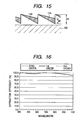
- the structure of the diffracting optical element used in each embodiment can be one selected, for example, from the single-layer structure comprised of one layer of the kinoform type as illustrated in Fig. 13 , the double-layer structure comprised of a stack of two layers having different (or equal) grating thicknesses as illustrated in Fig. 15 , and so on.
- Fig. 14 is a diagram to show wavelength dependence characteristics of diffraction efficiency of first-order diffracted light of the diffracting optical element 101 illustrated in Fig. 13 .
- the diffracting optical element 101 is made by applying an ultraviolet-curing resin onto a surface of substrate 102 and forming a layer 103 in such a grating thickness d that the diffraction efficiency of the first-order diffracted light becomes 100 % at the wavelength 530 nm, in the resin part.
- the diffraction efficiencies of the designed order decrease with departing from the wavelength 530 nm at which the diffraction efficiency is optimized, whereas diffraction efficiencies of the zero-order diffracted light and the second-order diffracted light of the orders close to the designed order increase.
- the increase of diffracted light other than the designed order will result in flares and in turn decrease in the resolution of the optical system.
- Fig. 16 shows the wavelength dependence characteristics of diffraction efficiency of the first-order diffracted light of the stack type diffracting optical element comprised of the stack of two layers 104, 105 illustrated in Fig. 15 .
- the diffracting optical element is of the stack structure, the diffraction efficiencies of the designed order are high, not less than 95 %, throughout the entire region of use wavelengths.
- the materials for the diffracting optical element in the stack structure described above are not limited to the ultraviolet-curing resins, but other plastic materials etc. can also be used, or the first layer 104 may be formed directly in the substrate, though depending upon the substrate.
- the grating thicknesses do not always have to be different from each other, but the grating thicknesses of the two layers 104 and 105 may also be equal to each other as illustrated in Fig. 17 , depending upon the combination of the materials.
- this structure since the grating shape is not formed in the surface of the diffracting optical element, this structure has an excellent dust-proofing property and can improve the assembling operability of the diffracting optical element.
- the present invention can accomplish the compact color image forming apparatus and scanning optical device suitable for high-resolution printing, the color image forming apparatus having a plurality of scanning optical devices, wherein the registration deviation in the sub-scanning direction among the colors can be suppressed by the simple structure to adjust the slant deviation of scanning line and the curve of scanning line in each scanning optical device by displacing the diffracting optical element of the diffraction section of each scanning optical device and wherein the image height deviation can be suppressed by the simple structure to adjust the asymmetric magnification (component of slope of magnification) in the main scanning direction on the image carrying member surface in each scanning optical device by displacing the refraction section or the scanning section including the refraction section and the deflecting element or/and the diffraction section of each scanning optical device in the main scanning direction.
- the simple structure to adjust the slant deviation of scanning line and the curve of scanning line in each scanning optical device by displacing the diffracting optical element of the diffraction section of each scanning optical
Landscapes
- Engineering & Computer Science (AREA)
- Multimedia (AREA)
- Signal Processing (AREA)
- Laser Beam Printer (AREA)
- Facsimile Scanning Arrangements (AREA)
- Mechanical Optical Scanning Systems (AREA)
Applications Claiming Priority (4)
| Application Number | Priority Date | Filing Date | Title |
|---|---|---|---|
| JP8501098 | 1998-03-16 | ||
| JP8501098 | 1998-03-16 | ||
| JP10152006A JPH11326804A (ja) | 1998-03-16 | 1998-05-15 | カラー画像形成装置及び走査光学装置 |
| JP15200698 | 1998-05-15 |
Publications (3)
| Publication Number | Publication Date |
|---|---|
| EP0944243A2 EP0944243A2 (en) | 1999-09-22 |
| EP0944243A3 EP0944243A3 (en) | 2000-11-15 |
| EP0944243B1 true EP0944243B1 (en) | 2014-06-04 |
Family
ID=26426052
Family Applications (1)
| Application Number | Title | Priority Date | Filing Date |
|---|---|---|---|
| EP99105248.1A Expired - Lifetime EP0944243B1 (en) | 1998-03-16 | 1999-03-15 | Color image forming apparatus and scanning optical apparatus |
Country Status (3)
| Country | Link |
|---|---|
| US (1) | US6452687B1 (enExample) |
| EP (1) | EP0944243B1 (enExample) |
| JP (1) | JPH11326804A (enExample) |
Families Citing this family (19)
| Publication number | Priority date | Publication date | Assignee | Title |
|---|---|---|---|---|
| JP2000111821A (ja) * | 1998-10-02 | 2000-04-21 | Konica Corp | 走査光学装置及び画像形成装置 |
| JP2001125027A (ja) * | 1999-10-28 | 2001-05-11 | Canon Inc | 走査光学装置とそれを用いたカラー画像形成装置 |
| JP4240777B2 (ja) * | 2000-08-01 | 2009-03-18 | キヤノン株式会社 | 走査光学装置及びそれを用いた画像形成装置 |
| JP4904617B2 (ja) | 2000-09-11 | 2012-03-28 | コニカミノルタホールディングス株式会社 | 画像形成装置 |
| JP4039797B2 (ja) | 2000-10-03 | 2008-01-30 | 株式会社リコー | 光走査装置および画像形成装置 |
| JP2002351086A (ja) * | 2001-03-22 | 2002-12-04 | Fuji Photo Film Co Ltd | 露光装置 |
| US20030174374A1 (en) * | 2001-12-11 | 2003-09-18 | Pentax Corporation | Scanning optical system |
| JP4027761B2 (ja) | 2002-09-11 | 2007-12-26 | ペンタックス株式会社 | 走査光学系 |
| US7301554B2 (en) * | 2002-09-20 | 2007-11-27 | Ricoh Company, Ltd. | Light scanning device, scanning line adjusting method, scanning line adjusting control method, image forming apparatus, and image forming method |
| JP4107578B2 (ja) * | 2002-12-13 | 2008-06-25 | 株式会社リコー | 画像形成装置 |
| US20040252748A1 (en) * | 2003-06-13 | 2004-12-16 | Gleitman Daniel D. | Fiber optic sensing systems and methods |
| US8824022B2 (en) | 2003-09-18 | 2014-09-02 | Ricoh Company, Ltd. | Optical scanning apparatus and image forming apparatus |
| JP4653404B2 (ja) * | 2004-03-01 | 2011-03-16 | 株式会社リコー | 光走査装置及び画像形成装置 |
| US6967608B1 (en) * | 2004-06-25 | 2005-11-22 | Texas Instruments Incorporated | Sigma-delta analog-to-digital converter (ADC) with truncation error cancellation in a multi-bit feedback digital-to-analog converter (DAC) |
| JP4502121B2 (ja) * | 2004-09-27 | 2010-07-14 | ブラザー工業株式会社 | 画像形成装置、カラー画像形成装置、走査ユニット及び走査レンズ |
| JP4689284B2 (ja) | 2005-01-21 | 2011-05-25 | 株式会社リコー | 光走査装置および画像形成装置 |
| JP2005258450A (ja) * | 2005-03-22 | 2005-09-22 | Ricoh Co Ltd | 光走査装置および画像形成装置 |
| JP5300505B2 (ja) | 2009-01-21 | 2013-09-25 | キヤノン株式会社 | 光走査装置の調整方法 |
| JP5342041B2 (ja) | 2011-07-11 | 2013-11-13 | キヤノン株式会社 | マルチビーム走査光学装置の組立調整方法及び製造方法 |
Family Cites Families (11)
| Publication number | Priority date | Publication date | Assignee | Title |
|---|---|---|---|---|
| EP1111430B1 (en) * | 1991-03-27 | 2005-12-28 | Fujitsu Limited | Light beam scanning apparatus |
| US5212501A (en) | 1991-04-30 | 1993-05-18 | Minolta Camera Kabushiki Kaisha | Image recording apparatus with a laser optical unit |
| US5315427A (en) | 1992-12-14 | 1994-05-24 | Xerox Corporation | Pair of binary diffraction optics for use in overfilled raster output scanning systems |
| US5422753A (en) | 1993-12-23 | 1995-06-06 | Xerox Corporation | Binary diffraction optical element for controlling scanning beam intensity in a raster output scanning (ROS) optical system |
| US5486694A (en) | 1994-12-02 | 1996-01-23 | Xerox Corporation | Wobble correction and focusing optical element with refractive toroidal surface and binary diffractive optical surface |
| US5838480A (en) * | 1996-04-29 | 1998-11-17 | The University Of Rochester | Optical scanning system with diffractive optics |
| US6088134A (en) | 1996-06-17 | 2000-07-11 | Hewlett-Packard Company | Swath scanning system using an optical imager |
| JP3432085B2 (ja) | 1996-08-28 | 2003-07-28 | キヤノン株式会社 | 走査光学装置 |
| JP3559710B2 (ja) | 1998-05-25 | 2004-09-02 | キヤノン株式会社 | 回折光学素子及びそれを用いた走査光学装置 |
| JP2000330050A (ja) | 1999-03-12 | 2000-11-30 | Canon Inc | マルチビーム走査光学装置及びカラー画像形成装置 |
| TW522714B (en) * | 2000-09-20 | 2003-03-01 | Ind Tech Res Inst | Optical scanning device |
-
1998
- 1998-05-15 JP JP10152006A patent/JPH11326804A/ja active Pending
-
1999
- 1999-03-12 US US09/266,826 patent/US6452687B1/en not_active Expired - Lifetime
- 1999-03-15 EP EP99105248.1A patent/EP0944243B1/en not_active Expired - Lifetime
Also Published As
| Publication number | Publication date |
|---|---|
| EP0944243A3 (en) | 2000-11-15 |
| EP0944243A2 (en) | 1999-09-22 |
| JPH11326804A (ja) | 1999-11-26 |
| US6452687B1 (en) | 2002-09-17 |
Similar Documents
| Publication | Publication Date | Title |
|---|---|---|
| EP0944243B1 (en) | Color image forming apparatus and scanning optical apparatus | |
| JP3375196B2 (ja) | 光走査装置およびこの光走査装置に適した画像形成装置 | |
| US7561319B2 (en) | Optical scanning device and image forming apparatus using the same | |
| JP4039797B2 (ja) | 光走査装置および画像形成装置 | |
| US20080170282A1 (en) | Optical scanning device, image forming apparatus and liquid crystal device driving method | |
| US8217980B2 (en) | Multi-beam optical scanning device and image forming apparatus using the same | |
| US7380720B2 (en) | Optical scanning system and image forming apparatus using the same | |
| US7768542B2 (en) | Multi-beam optical scanning device and image forming apparatus using the same | |
| US20080165244A1 (en) | Optical scanning device and image forming apparatus using the same | |
| JP3569412B2 (ja) | 多色画像形成装置の光走査装置 | |
| JP2004070107A (ja) | 光走査装置及びそれを用いた画像形成装置 | |
| US20050045814A1 (en) | Optical scanning device and image forming apparatus using the same | |
| EP1336889B1 (en) | Scanning optical apparatus and image forming apparatus using the same | |
| US7550712B2 (en) | Optical scanning system with reduced spherical aberration and image forming apparatus using the same | |
| US6980343B2 (en) | Optical scanning apparatus and image forming apparatus using the same | |
| US20060055995A1 (en) | Optical scanning apparatus and image forming apparatus using the same | |
| US6603500B2 (en) | Scanning optical apparatus with aspherically-shaped surface in main scanning direction | |
| US7508563B2 (en) | Optical scanning device and image forming apparatus using the same | |
| US7136208B2 (en) | Light scanning apparatus and image forming apparatus using the same | |
| US7034972B2 (en) | Optical scanning device and image forming apparatus using the optical scanning device | |
| US7304778B2 (en) | Optical scanning system and image forming apparatus using the same | |
| JP4546118B2 (ja) | 光走査装置及びそれを用いたカラー画像形成装置 | |
| JP2001088351A (ja) | 画像形成装置 | |
| JPH09184991A (ja) | 光走査装置並びにこの光走査装置を利用した画像形成装置 | |
| JP2000141759A (ja) | カラー画像形成装置 |
Legal Events
| Date | Code | Title | Description |
|---|---|---|---|
| PUAI | Public reference made under article 153(3) epc to a published international application that has entered the european phase |
Free format text: ORIGINAL CODE: 0009012 |
|
| AK | Designated contracting states |
Kind code of ref document: A2 Designated state(s): DE FR GB IT |
|
| AX | Request for extension of the european patent |
Free format text: AL;LT;LV;MK;RO;SI |
|
| PUAL | Search report despatched |
Free format text: ORIGINAL CODE: 0009013 |
|
| AK | Designated contracting states |
Kind code of ref document: A3 Designated state(s): AT BE CH CY DE DK ES FI FR GB GR IE IT LI LU MC NL PT SE |
|
| AX | Request for extension of the european patent |
Free format text: AL;LT;LV;MK;RO;SI |
|
| 17P | Request for examination filed |
Effective date: 20010515 |
|
| AKX | Designation fees paid |
Free format text: DE FR GB IT |
|
| 17Q | First examination report despatched |
Effective date: 20041216 |
|
| GRAP | Despatch of communication of intention to grant a patent |
Free format text: ORIGINAL CODE: EPIDOSNIGR1 |
|
| INTG | Intention to grant announced |
Effective date: 20131209 |
|
| GRAS | Grant fee paid |
Free format text: ORIGINAL CODE: EPIDOSNIGR3 |
|
| GRAA | (expected) grant |
Free format text: ORIGINAL CODE: 0009210 |
|
| AK | Designated contracting states |
Kind code of ref document: B1 Designated state(s): DE FR GB IT |
|
| REG | Reference to a national code |
Ref country code: GB Ref legal event code: FG4D |
|
| REG | Reference to a national code |
Ref country code: DE Ref legal event code: R096 Ref document number: 69945111 Country of ref document: DE Effective date: 20140717 |
|
| REG | Reference to a national code |
Ref country code: DE Ref legal event code: R097 Ref document number: 69945111 Country of ref document: DE |
|
| PLBE | No opposition filed within time limit |
Free format text: ORIGINAL CODE: 0009261 |
|
| STAA | Information on the status of an ep patent application or granted ep patent |
Free format text: STATUS: NO OPPOSITION FILED WITHIN TIME LIMIT |
|
| PG25 | Lapsed in a contracting state [announced via postgrant information from national office to epo] |
Ref country code: IT Free format text: LAPSE BECAUSE OF FAILURE TO SUBMIT A TRANSLATION OF THE DESCRIPTION OR TO PAY THE FEE WITHIN THE PRESCRIBED TIME-LIMIT Effective date: 20140604 |
|
| 26N | No opposition filed |
Effective date: 20150305 |
|
| PGFP | Annual fee paid to national office [announced via postgrant information from national office to epo] |
Ref country code: GB Payment date: 20150311 Year of fee payment: 17 |
|
| REG | Reference to a national code |
Ref country code: DE Ref legal event code: R097 Ref document number: 69945111 Country of ref document: DE Effective date: 20150305 |
|
| PGFP | Annual fee paid to national office [announced via postgrant information from national office to epo] |
Ref country code: DE Payment date: 20150331 Year of fee payment: 17 |
|
| REG | Reference to a national code |
Ref country code: FR Ref legal event code: ST Effective date: 20151130 |
|
| PG25 | Lapsed in a contracting state [announced via postgrant information from national office to epo] |
Ref country code: FR Free format text: LAPSE BECAUSE OF NON-PAYMENT OF DUE FEES Effective date: 20150331 |
|
| REG | Reference to a national code |
Ref country code: DE Ref legal event code: R119 Ref document number: 69945111 Country of ref document: DE |
|
| GBPC | Gb: european patent ceased through non-payment of renewal fee |
Effective date: 20160315 |
|
| PG25 | Lapsed in a contracting state [announced via postgrant information from national office to epo] |
Ref country code: DE Free format text: LAPSE BECAUSE OF NON-PAYMENT OF DUE FEES Effective date: 20161001 Ref country code: GB Free format text: LAPSE BECAUSE OF NON-PAYMENT OF DUE FEES Effective date: 20160315 |