EP0942552A2 - Circuit de récupération d'horloge à sur-échantillonnage avec consommation d'énergie réduite - Google Patents
Circuit de récupération d'horloge à sur-échantillonnage avec consommation d'énergie réduite Download PDFInfo
- Publication number
- EP0942552A2 EP0942552A2 EP99103810A EP99103810A EP0942552A2 EP 0942552 A2 EP0942552 A2 EP 0942552A2 EP 99103810 A EP99103810 A EP 99103810A EP 99103810 A EP99103810 A EP 99103810A EP 0942552 A2 EP0942552 A2 EP 0942552A2
- Authority
- EP
- European Patent Office
- Prior art keywords
- clock signals
- phase
- sets
- signal
- phase difference
- Prior art date
- Legal status (The legal status is an assumption and is not a legal conclusion. Google has not performed a legal analysis and makes no representation as to the accuracy of the status listed.)
- Withdrawn
Links
Images


Classifications
-
- H—ELECTRICITY
- H03—ELECTRONIC CIRCUITRY
- H03L—AUTOMATIC CONTROL, STARTING, SYNCHRONISATION, OR STABILISATION OF GENERATORS OF ELECTRONIC OSCILLATIONS OR PULSES
- H03L7/00—Automatic control of frequency or phase; Synchronisation
- H03L7/06—Automatic control of frequency or phase; Synchronisation using a reference signal applied to a frequency- or phase-locked loop
-
- H—ELECTRICITY
- H04—ELECTRIC COMMUNICATION TECHNIQUE
- H04L—TRANSMISSION OF DIGITAL INFORMATION, e.g. TELEGRAPHIC COMMUNICATION
- H04L7/00—Arrangements for synchronising receiver with transmitter
- H04L7/02—Speed or phase control by the received code signals, the signals containing no special synchronisation information
- H04L7/033—Speed or phase control by the received code signals, the signals containing no special synchronisation information using the transitions of the received signal to control the phase of the synchronising-signal-generating means, e.g. using a phase-locked loop
- H04L7/0337—Selecting between two or more discretely delayed clocks or selecting between two or more discretely delayed received code signals
-
- Y—GENERAL TAGGING OF NEW TECHNOLOGICAL DEVELOPMENTS; GENERAL TAGGING OF CROSS-SECTIONAL TECHNOLOGIES SPANNING OVER SEVERAL SECTIONS OF THE IPC; TECHNICAL SUBJECTS COVERED BY FORMER USPC CROSS-REFERENCE ART COLLECTIONS [XRACs] AND DIGESTS
- Y10—TECHNICAL SUBJECTS COVERED BY FORMER USPC
- Y10S—TECHNICAL SUBJECTS COVERED BY FORMER USPC CROSS-REFERENCE ART COLLECTIONS [XRACs] AND DIGESTS
- Y10S331/00—Oscillators
- Y10S331/02—Phase locked loop having lock indicating or detecting means
Definitions
- the present invention relates to a clock recovery circuit, and more particularly, to an over-sampling type clock recovery circuit which performs sampling of a data signal based on a plurality of clock signals having different phases.
- a high-speed protocol such as Gbit Ethernet and Fiber Channel for data transmission.
- high speed processing is requested in a clock recovery circuit to extract a clock signal from a data signal in a high speed transmission and in a PLL circuit to establish frequency synchronization between the clock signal used in the circuit and the transmitted clock signal.
- a clock recovery circuit to extract a clock signal from a data signal in a high speed transmission and in a PLL circuit to establish frequency synchronization between the clock signal used in the circuit and the transmitted clock signal.
- an over-sampling type clock recovery circuit is proposed in which the transmitted data signal is sampled based on a plurality of clock signals with different phases generated by an internal circuit.
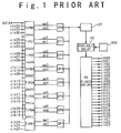
- Fig. 1 shows a circuit block diagram of a clock recovery circuit which is disclosed in the conventional example.
- a data signal is supplied to eight phase comparators TIPD0 to TIPD7.
- the respective phase comparators TIPD0 to TIPD7 are supplied with 24 clock signals having fixed delays outputted from a fixed delay circuit for every set of three clock signals.
- Each phase comparator detects the phase state between the data signal and the set of three clock signals.
- the phase comparator detects the leading of the clock signals to set a corresponding one of dn signals dn0 to dn7 to an enable state and a corresponding one of up signals up0 to up7 to a disable state.
- the phase comparator sets the dn signal to the disable state and the up signal to the enable state.
- Charge pumps CP0 to CP7 increase the output voltages when the up signals are set to the enable state and decrease the output voltages decrease when the dn signal is set to the enable state.
- the output voltages are supplied to a low pass filter LPF.
- the low pass filter LPF integrates the changes of these voltages and outputs the integrated voltage to a variable delay circuit VD.
- a voltage controlled oscillator VCO oscillates and generates a basic clock signal to output to the variable delay circuit VD.
- the variable delay circuit VD delays the basic clock signal from the voltage controlled oscillator VCO in accordance with the integrated voltage from the low pass filter LPF.
- a fixed delay circuit FD receives the delayed clock signal from the variable delay circuit FD and generates the 24 clock signals having fixed delays from the delayed clock signal.
- the up signal or dn signal is set to the enable state in each phase comparator.
- the voltage outputted from the corresponding charge pump CP increases or decreases, when the leading or delaying states of the set of clock signals is detected. Therefore, the delayed clock signal is outputted from the variable delay circuit VD based on the phase leading or delaying state, and the 24 clock signals are generated by the fixed delay circuit FD based on the delayed clock signal.
- the leading or delaying state of the clock signals to be supplied to each of the phase comparators TIPD0 to TIPD7 is controlled so that the appropriate sampling of the data signal can be realized.
- the eight phase comparators TIPD0 to TIPD7 are always in the operating state regardless of whether or not they are in the locking state. As the result, in the locking state, ones of the phase comparators other than the phase comparators necessary to detect phase differences perform unnecessary operation. Therefore, the eight phase comparators with the relatively large power consumption operate continuously at the same time. Thus, the power consumption as the whole clock recovery circuit cannot be ignored. Also, each of the charge pumps CP0 to CP7 subsequent to the phase comparators TIPD0 to TIPD7 operate based on phase difference data outputted from the respective phase comparators. Moreover, the power consumption in the low pass filter LPF and the subsequent circuits cannot be ignored.
- a transmission path signal receiving system is disclosed in Japanese Laid Open Patent Application (JP-A-Heisei 3-92033).
- the transmission path signal receiving system is composed of a signal converting section, a reference clock generating section, a determining section, and clock reproducing section.
- the signal converting section converts the transmission path signal into a logic signal.
- the reference clock generating section generates a reference clock signal having a frequency higher than a bit rate of a digital data of the transmission path signal.
- the determining section performs over-sampling and a logic process to the logic signal using the reference clock signal and determines a value of the digital data.
- the clock reproducing section inserts a predetermined pulse into the logic signal in accordance with the determining result of the determining section to reproduce a clock signal.
- a data receiving apparatus is disclosed in Japanese Laid Open Patent Application (JP-A-Heisei 8-317007).
- the data receiving apparatus is composed of an A/D converting section 24, an adding section 25, a detecting section 26, a demodulating section 27, a detecting section 28, a variable frequency dividing section 30, a control section 29, frame sync signals generating sections 31 and 32.
- the A/D converting section 24 performs over-sampling of a reception signal based on a free-running clock signal having a frequency of integer times of a symbol rate to convert the sampling values into digital values.
- the adding section 25 adding the digital sampling values synchronously for a symbol period over a predetermined period.
- the detecting section 26 detects a symbol identifying point from the synchronously adding result.
- the demodulating section 27 performs data demodulation based on the sample value at the symbol identifying point.
- the detecting section 28 detects the displacement of the symbol identifying point accompanied with time as a phase shift.
- the variable frequency dividing section 30 divides the free-running clock signal in frequency to reproduce a bit clock signal.
- the control section 29 controls a frequency division ratio of the variable frequency dividing section 30 to correct a phase shift.
- the frame sync signals generating sections 31 and 32 extract a known sync word from the demodulated data to establish a frame synchronization, and generate a frame sync timing signal based on the extracted sync word.
- An object of the present invention is to provide an over-sampling type clock recovery circuit in which an unnecessary operation is stopped in a locking state.
- Another object of the present invention is to provide an over-sampling type clock recovery circuit in which the power consumption can be reduced.
- an over-sampling type clock recovery circuit includes a phase difference detecting section, a phase adjusting section, and a signal selecting section.
- the phase difference detecting section detects a phase difference between a data signal and each of a plurality of active sets of clock signals, and generates a phase adjustment signal from a plurality of phase difference data corresponding to the detected phase differences.
- the phase adjusting section generates N (N is an integer equal to or larger than 2) sets of clock signals and adjusts phases of clock signals of the N sets based on the phase adjustment signal.
- the signal selecting section selects a part or all of the N sets of clock signals based on the detected phase differences from the phase difference detecting section and supplies the selected sets of clock signals to the phase difference detecting section as the plurality of active sets of clock signals.
- the phase adjusting section may include an oscillator for generating a reference clock signal, a delay unit for delaying the reference clock signal based on the phase adjustment signal, and a clock signal generating section for generating the N sets of clock signals from the delayed reference signal such that each of the plurality of clock signals has a predetermined delay.
- the phase difference detecting section may include N phase comparators.
- the plurality of active sets of clock signals are supplied to selected ones of the N phase comparators, and each of the selected phase comparators compares a corresponding one of bits of the data signal and a corresponding one of the plurality of active sets of clock signals in phase to detect the phase difference and for generating the phase difference data based on the detected phase difference.
- the phase difference detecting section may further include an adjustment signal generating section for generating the phase adjustment signal from the plurality of phase difference data from the selected phase comparators.
- non-selected phase comparators of the N phase comparators other than the selected phase comparators stop their operations to reduce power consumption.
- a portion of the adjustment signal generating section corresponding to the non-selected phase comparators stops its operation to reduce power consumption.
- the part of the N sets of clock signals is preferably predetermined.
- the signal selecting section selects all of the N sets of clock signals when any one of the plurality of phase difference data indicates that the data signal and a corresponding one of the plurality of active sets of clock signals are not matched to each other in phase, and the part of the N sets of clock signals when all of the phase differences indicate that the data signal and a corresponding one of the plurality of active sets of clock signals are matched to each other in phase.
- the signal selecting section may include a locking state detecting circuit and a switch circuit.
- the locking state detecting circuit determines based on the plurality of phase difference data supplied from the phase difference detecting section whether the data signal and each of the plurality of active sets of clock signals are matched to each other in phase.
- the switch circuit supplies all of the N sets of clock signals to the phase difference detecting section as the plurality of active sets of clock signals when the locking state detecting circuit detects that the data signal and at least one of the plurality of active sets of clock signals are not matched to each other in phase.
- the switch circuit fixes the clock signals of as non-selected sets as ones of the N sets other than the selected sets to a high or low level, when the locking state detecting circuit detects that the data signal and each of the plurality of active sets of clock signals are matched to each other in phase, and supplies the selected sets of clock signals and the non-selected sets of clock signals to the phase difference detecting section.
- a method of adjusting phases of clock signals in an over-sampling type clock recovery circuit comprising:
- Fig. 2 is a block circuit diagram illustrating the structure of an over-sampling type clock recovery circuit according to an embodiment of the present invention. It should be noted that the same reference numerals are allocated to the same components as those of the conventional clock recovery circuit.
- the over-sampling type clock recovery circuit in the embodiment is composed of eight phase comparators TIPD0 to TIPD7, charge pumps CP0 to CP7, a low pass filter LPF, a variable delay circuit VD, a voltage controlled oscillator VCO, a fixed delay circuit FD, a locking state detecting circuit LDEC, and a switch circuit SW.
- the phase comparators TIPD0 to TIPD7 are provided to perform sampling of a data signal of 8 bits with three clock signals. That is, each of the comparators TIPD0 to TIPD7 inputs the clock signals having the same fixed delay and the transmitted data signal and detects the phase state between the data signal and clock signals to output a phase difference data corresponding to the detected phase state.
- Figs. 4A to 4F show a locking state in which the phases of the data signal and the clock signals are coincident with each other in phase.
- Figs. 5A to 5F show the clock delaying state in which the data signal leads the clock signals.
- the phase comparator detects the clock leading state to set an up signal of the phase difference data to an enable state and to set a dn signal of the phase difference data to a disable state.
- Figs. 6A to 6F show the clock leading state in which the data signal delays than the clock signals.
- the phase comparator detects the clock leading state to set the up signal to a disable state and to set the dn signal to an enable state.
- the respective charge pumps CP and the single locking state detecting circuit LDEC are connected to the output terminals of said phase comparators TIPD for the up signals and the dn signals in parallel.
- the locking state detecting circuit LDEC recognizes the locking state of each phase comparator from the phase states of the up signal and dn signal outputted from each phase comparator, and detects whether all the phase comparators, i.e. the whole circuit is set to the locking state. Then, the locking state detecting circuit LDEC outputs a locking state detection signal switched between the enable state and the disable state based on the detection result of the locking state.
- the charge pumps CP0 to CP7 input the up signals and the dn signals from the phase comparators TIPD0 to TIPD7 and changes the output voltage in accordance with the up signals and the dn signals to output to the low pass filter LPF.
- the low pass filter LPF integrates the changes of the output voltages from the charge pumps CP0 to CP7 to output to the variable delay circuit VD.
- the variable delay circuit VD inputs a reference clock signal having a predetermined frequency supplied from the voltage controlled oscillator VCO and the output of the low pass filter LPF, and delays the reference clock signal in accordance with the output voltage of the low pass filter LPF.
- the fixed delay circuit FD inputs the output of the variable delay circuit VD, and generates 24 clock signals clk00 to 23 having fixed delays from the delayed reference clock signal to supply to the phase comparators TIPD0 to TIPD7 for every three clock signals.
- the switch circuit SW is connected to the output terminals of the fixed delay circuit FD for the 24 clock signals such that the level of each clock signal is selectively set to a high level or a low level, to the high level in this example.
- the switch circuit SW fixes predetermined ones of the 24 clock signals clk00 to clk23 as selected clock signals to the high level.
- the clock signals fixed to the high level are predetermined for every set of three clock signals to be supplied to the phase comparator. Therefore, only the clock signals supplied to the selected ones of the phase comparators TIPD0 to TIPD7 are fixed to the high level.
- Non-selected clock signals of the 24 clock signals other than the selected clock signals are supplied, as they are, to non-selected ones of the phase comparators TIPD0 to TIPD7 other than the selected phase comparators through the switch circuit SW.
- the switch circuit SW supplies the 24 clock signals clk00 to clk23 to the phase comparators TIPD0 to TIPD7, as they are.
- Figs. 3A to 3Y are time charts to explain the data signal supplied to the eight phase comparators and the 24 clock signals used to perform sampling of the supplied data signal. Since there is no need to change the phase of the clock signals in the locking state, both of the up signal and dn signal of the phase difference data are set to the disable state. When the clock signals delay than the data signal, the up signal is set to the enable state and the dn signal is set to the disable state, so that the phases of the clock signals are led. On contrary, when the clock signals lead the data signal, the up signal is set to the disable state and the dn signal is set to the enable state, so that the phases of the clock signals are delayed.
- the up signals and dn signals are supplied from the respective phase comparators TIPD0 to TIPD7 to the respective charge pumps CP0 to CP7 and the single locking state detecting circuit LDEC, respectively.
- the phase difference data obtained from these up signals and the dn signals are converted into the voltage value. That is, the output voltage is increased when the up signal is set to the enable state, and the output voltage is decreased when the dn signal is set to the enable state.
- the low pass filter LPF inputs the output voltages from the charge pumps CP0 to CP7 and integrates the changes of the voltages.
- the variable delay circuit VD inputs the output voltage of low pass filter LPF and the reference clock signal which is the output of the voltage controlled oscillator VCO, and delays and outputs the reference clock signal in accordance with the output voltage of the low pass filter LPF.
- the relation of a delay quantity to the input voltage from the variable delay circuit VD is shown in Fig. 7.
- the delayed reference clock signal is supplied from the variable delay circuit VD to the fixed delay circuit FD.
- the fixed delay circuit FD generates the 24 clock signals clk00 to clk23 which have the same phase differences between them from the delayed reference clock signal to output to the phase comparators TIPD.
- the locking state detecting circuit LDEC inputs the up signals and the dn signals from the phase comparators TIPD.
- the locking state detecting circuit LDEC recognizes the detection results of the respective phase comparators TIPD0 to TIPD7 based on the up signals and the dn signals, that is, the respective phase states from the phase difference data. Then, when all the up signals and all the dn signals are set to the disable, in other words, the locking states are detected, the locking state detecting circuit LDEC outputs a locking state indication signal set to an enable state to the switch circuit SW.
- the locking state detecting circuit LDEC when at least one of the up signals and dn signals outputted from the phase comparators TIPD is set to the enable state, i.e., in a non-locking state, the locking state detecting circuit LDEC outputs a locking state indication signal set to a disable state.
- Figs. 8A to 8AA show timing charts to explain the operation of the switch circuit SW based on the enable state and the disable state of the locking state indication signal from the locking state detecting circuit LDEC.
- the switch circuit SW supplies all of the 24 clocks supplied from the fixed delay circuit FD to the respective phase comparators TIPD in response to the locking state indication signal of the disable state.
- the switch circuit SW sends only the selected ones of the 24 clock signals to selected ones of the phase comparators TIPD, just as they are, in response to the enable output.
- the switch circuit SW fixes the non-selected clock signals to the high state.
- the switch circuit SW supplies 9 clock signals clk00 to clk08 to the phase comparators TIPD0 to TIPD2 in case of the locking state.
- the switch circuit SW fixes the other 15 clock signals clk09 to clk23 to the high level and supplies them to the phase comparators TIPD3 to TIPD7, respectively. That is, these phase comparators TIPD3 to TIPD7 are set to the states equivalent to the state in which any clock signal is not supplied.
- the number of data bits of the transmitted data signal which continuously have the same value is defined depending upon the transmission system. Therefore, even if the number of clock signals used for sampling in the locking state is reduced, the detection of the phase difference is normally performed.
- the phase comparators TIPD0 to TIPD2 to which the clock signals are supplied in the locking state performs the phase detection as in the non-locking state. When any clock signal is not supplied, the phase comparator does not perform the phase difference detecting operation and the phase comparator TIPD maintains the locking state regardless of the phase difference between the data signal and the clock signals. As shown in Figs. 4A to 4F, the phase comparator needs the change point (the edge) of the clock signals supplied for the sampling of the data signal.
- the phase comparators TIPD3 to TIPD7 are set to the state in which the phase detecting operation is stopped so that power consumption can be reduced.
- the switch circuit SW again supplies all the clock signals which are not fixed to the high level, to the respective phase comparators TIPD0 to TIPD7. This is because the locking state detecting circuit LDEC outputs the locking state indication signal of the disable state. This is performed until all the phase comparators TIPD0 to TIPD7 are set to the locking state again.
- the locking stated of the phase comparators are detected by the locking state detecting circuit LDEC.
- the non-locking state all the clock signals generated by the fixed delay circuit FD are supplied to the phase comparators TIPD0 to TIPD7, whereas, only the selected ones of the clock signals are supplied to the selected ones of the phase comparators in the locking state.
- the operations of the selected phase comparators are set to the stopped state.
- the charge pumps CP connected with the selected phase comparators are set to the state in which the operations are set to the stopped state. Therefore, it is possible to decrease the power consumption of the whole clock recovery circuit in the locking state. The total power consumption of the whole circuit can be reduced.
- the embodiment shows an example of the present invention only. It is possible to suitably set the number of clock signals to be fixed to the high level in the locking state and the number of phase comparators. Also, in the locking state, the selected clock signals may be fixed to the low level. Further, it would not need to say that the number of bits of the data signal and the number of phase comparators associated with this number of bits of the data signal and the number of clock signals having the fixed phases used for phase comparison can be set suitably in accordance with the required speed.
- the locking state of each phase comparator is detected by the locking state detecting circuit based on the phase difference data between the data signal and the clock signals outputted from the plurality of ⁇ phase comparators.
- the non-locking state all clock signals are supplied to the respective phase comparators.
- the selected clock signals are fixed to the high level or the low level and the selected clock signals are supplied to only the selected phase comparators. Therefore, in the locking state, the operations of the selected phase comparators are set to the stopped state.
- the circuit elements connected with the phase comparators are set to the state in which the operations are set to the stopped state. Therefore, it is possible to reduce the power consumption of the whole clock recovery circuit in the locking state. The total power consumption of the whole circuit can be reduced.
Applications Claiming Priority (2)
| Application Number | Priority Date | Filing Date | Title |
|---|---|---|---|
| JP6173798 | 1998-03-12 | ||
| JP6173798A JP3077661B2 (ja) | 1998-03-12 | 1998-03-12 | オーバーサンプリング型クロックリカバリ回路 |
Publications (2)
| Publication Number | Publication Date |
|---|---|
| EP0942552A2 true EP0942552A2 (fr) | 1999-09-15 |
| EP0942552A3 EP0942552A3 (fr) | 2003-12-17 |
Family
ID=13179818
Family Applications (1)
| Application Number | Title | Priority Date | Filing Date |
|---|---|---|---|
| EP99103810A Withdrawn EP0942552A3 (fr) | 1998-03-12 | 1999-02-26 | Circuit de récupération d'horloge à sur-échantillonnage avec consommation d'énergie réduite |
Country Status (5)
| Country | Link |
|---|---|
| US (1) | US6124762A (fr) |
| EP (1) | EP0942552A3 (fr) |
| JP (1) | JP3077661B2 (fr) |
| KR (1) | KR100297155B1 (fr) |
| CN (1) | CN1129231C (fr) |
Families Citing this family (11)
| Publication number | Priority date | Publication date | Assignee | Title |
|---|---|---|---|---|
| JP3755564B2 (ja) * | 1999-05-24 | 2006-03-15 | 株式会社村田製作所 | 圧電共振部品及びその製造方法 |
| JP4425426B2 (ja) * | 2000-05-11 | 2010-03-03 | Necエレクトロニクス株式会社 | オーバーサンプリング型クロックリカバリ回路 |
| US6545507B1 (en) * | 2001-10-26 | 2003-04-08 | Texas Instruments Incorporated | Fast locking CDR (clock and data recovery circuit) with high jitter tolerance and elimination of effects caused by metastability |
| CN100358238C (zh) * | 2002-09-02 | 2007-12-26 | 瑞昱半导体股份有限公司 | 资料回复系统及其方法 |
| EP1566806A4 (fr) * | 2002-11-29 | 2007-09-05 | Fujitsu Ltd | Appareil de reproduction de donnees a correcteur de difference de phase et a detecteur de donnees a tete de lecture/ecriture |
| JP4668750B2 (ja) | 2005-09-16 | 2011-04-13 | 富士通株式会社 | データ再生回路 |
| US20080084955A1 (en) * | 2006-10-10 | 2008-04-10 | Wei-Zen Chen | Fast-locked clock and data recovery circuit and the method thereof |
| JP2009094638A (ja) * | 2007-10-04 | 2009-04-30 | Yokogawa Electric Corp | 高周波モジュール |
| JP5363967B2 (ja) * | 2009-12-22 | 2013-12-11 | ルネサスエレクトロニクス株式会社 | クロックデータリカバリ回路、表示装置用データ転送装置及び表示装置用データ転送方法 |
| JP2013123174A (ja) * | 2011-12-12 | 2013-06-20 | Mitsubishi Electric Corp | クロック再生装置およびクロック再生方法 |
| JP6724619B2 (ja) | 2016-07-15 | 2020-07-15 | 富士通株式会社 | 信号再生回路、電子装置及び信号再生方法 |
Citations (3)
| Publication number | Priority date | Publication date | Assignee | Title |
|---|---|---|---|---|
| US4841255A (en) * | 1987-06-24 | 1989-06-20 | Matsushita Electric Industrial Co., Ltd. | Frequency synthesizer |
| EP0402736A2 (fr) * | 1989-06-14 | 1990-12-19 | Fujitsu Limited | Circuit détecteur de différence de phase |
| US5428317A (en) * | 1994-09-06 | 1995-06-27 | Motorola, Inc. | Phase locked loop with low power feedback path and method of operation |
Family Cites Families (2)
| Publication number | Priority date | Publication date | Assignee | Title |
|---|---|---|---|---|
| JPH0392033A (ja) * | 1989-09-04 | 1991-04-17 | Nec Corp | 伝送路信号受信方式 |
| JP3064867B2 (ja) * | 1995-05-23 | 2000-07-12 | 松下電器産業株式会社 | データ受信装置 |
-
1998
- 1998-03-12 JP JP6173798A patent/JP3077661B2/ja not_active Expired - Fee Related
-
1999
- 1999-02-26 EP EP99103810A patent/EP0942552A3/fr not_active Withdrawn
- 1999-03-11 KR KR1019990008115A patent/KR100297155B1/ko not_active IP Right Cessation
- 1999-03-12 CN CN99102997A patent/CN1129231C/zh not_active Expired - Fee Related
- 1999-03-12 US US09/266,886 patent/US6124762A/en not_active Expired - Fee Related
Patent Citations (3)
| Publication number | Priority date | Publication date | Assignee | Title |
|---|---|---|---|---|
| US4841255A (en) * | 1987-06-24 | 1989-06-20 | Matsushita Electric Industrial Co., Ltd. | Frequency synthesizer |
| EP0402736A2 (fr) * | 1989-06-14 | 1990-12-19 | Fujitsu Limited | Circuit détecteur de différence de phase |
| US5428317A (en) * | 1994-09-06 | 1995-06-27 | Motorola, Inc. | Phase locked loop with low power feedback path and method of operation |
Non-Patent Citations (1)
| Title |
|---|
| INYEOL LEE ET AL: "A 622 Mb/s CMOS clock recovery PLL with time-interleaved phase detector array" SOLID-STATE CIRCUITS CONFERENCE, 1996. DIGEST OF TECHNICAL PAPERS. 42ND ISSCC., 1996 IEEE INTERNATIONAL SAN FRANCISCO, CA, USA 8-10 FEB. 1996, NEW YORK, NY, USA,IEEE, US, 8 February 1996 (1996-02-08), pages 198-199,444, XP010156453 ISBN: 0-7803-3136-2 * |
Also Published As
| Publication number | Publication date |
|---|---|
| CN1234653A (zh) | 1999-11-10 |
| US6124762A (en) | 2000-09-26 |
| CN1129231C (zh) | 2003-11-26 |
| JPH11261409A (ja) | 1999-09-24 |
| JP3077661B2 (ja) | 2000-08-14 |
| KR100297155B1 (ko) | 2001-09-26 |
| KR19990077789A (ko) | 1999-10-25 |
| EP0942552A3 (fr) | 2003-12-17 |
Similar Documents
| Publication | Publication Date | Title |
|---|---|---|
| US5950115A (en) | GHz transceiver phase lock loop having autofrequency lock correction | |
| US5539784A (en) | Refined timing recovery circuit | |
| EP0346896B1 (fr) | Convertisseur parallèle-série | |
| EP0317159A2 (fr) | Dispositif de récupération d'horloge | |
| JPH08163117A (ja) | ビット位相同期回路 | |
| US6124762A (en) | Over-sampling type clock recovery circuit with power consumption reduced | |
| US7120216B2 (en) | Data/clock recovery circuit for recovering data and clock signal with high accuracy | |
| US6130584A (en) | Over-sampling type clock recovery circuit with power consumption reduced | |
| US5694062A (en) | Self-timed phase detector and method | |
| EP0878911B1 (fr) | Circuit d'extraction d'un signal d'horloge | |
| JPH07336342A (ja) | クロック再生回路 | |
| US7194057B2 (en) | System and method of oversampling high speed clock/data recovery | |
| US6222419B1 (en) | Over-sampling type clock recovery circuit using majority determination | |
| US6577167B1 (en) | Clock signal producing circuit immediately producing clock signal synchronized with input signal | |
| US6337650B1 (en) | System and method for regenerating clock signal | |
| US5463664A (en) | DQPSK delay detection circuit that produces stable clock signal in response to both I and Q signals | |
| JP5000635B2 (ja) | 多ピン非同期シリアル・インタフェース全体に転送されるデータをビット同期する方法および装置 | |
| US6218907B1 (en) | Frequency comparator and PLL circuit using the same | |
| JP2000228660A (ja) | クロック再生/識別装置 | |
| JP3001836B2 (ja) | ディジタル位相同期回路 | |
| KR19980033965A (ko) | 광통신 수신기용 클럭 및 데이타(Data) 복구회로 | |
| JPH08237104A (ja) | ビット位相検出回路およびビット位相同期回路 | |
| US20020175721A1 (en) | Frame synchronism detection circuit | |
| KR100194753B1 (ko) | 디지탈 위상고정루프(dpll)를 이용한 비동기 데이타 동기식 변환장치 및 그 방법 | |
| KR100465298B1 (ko) | 사설 교환기의 입력 신호 선택 방법 및 장치 |
Legal Events
| Date | Code | Title | Description |
|---|---|---|---|
| PUAI | Public reference made under article 153(3) epc to a published international application that has entered the european phase |
Free format text: ORIGINAL CODE: 0009012 |
|
| AK | Designated contracting states |
Kind code of ref document: A2 Designated state(s): AT BE CH CY DE DK ES FI FR GB GR IE IT LI LU MC NL PT SE |
|
| AX | Request for extension of the european patent |
Free format text: AL;LT;LV;MK;RO;SI |
|
| RAP1 | Party data changed (applicant data changed or rights of an application transferred) |
Owner name: NEC ELECTRONICS CORPORATION |
|
| PUAL | Search report despatched |
Free format text: ORIGINAL CODE: 0009013 |
|
| AK | Designated contracting states |
Kind code of ref document: A3 Designated state(s): AT BE CH CY DE DK ES FI FR GB GR IE IT LI LU MC NL PT SE |
|
| AX | Request for extension of the european patent |
Extension state: AL LT LV MK RO SI |
|
| RIC1 | Information provided on ipc code assigned before grant |
Ipc: 7H 03L 7/087 B Ipc: 7H 03L 7/08 B Ipc: 7H 04L 7/033 A |
|
| 17P | Request for examination filed |
Effective date: 20031110 |
|
| 17Q | First examination report despatched |
Effective date: 20040216 |
|
| AKX | Designation fees paid |
Designated state(s): DE FR GB |
|
| STAA | Information on the status of an ep patent application or granted ep patent |
Free format text: STATUS: THE APPLICATION IS DEEMED TO BE WITHDRAWN |
|
| 18D | Application deemed to be withdrawn |
Effective date: 20040629 |