EP0931379B1 - Pompe a charge avec trois puits - Google Patents
Pompe a charge avec trois puits Download PDFInfo
- Publication number
- EP0931379B1 EP0931379B1 EP96939448A EP96939448A EP0931379B1 EP 0931379 B1 EP0931379 B1 EP 0931379B1 EP 96939448 A EP96939448 A EP 96939448A EP 96939448 A EP96939448 A EP 96939448A EP 0931379 B1 EP0931379 B1 EP 0931379B1
- Authority
- EP
- European Patent Office
- Prior art keywords
- transistor
- charge pump
- transistors
- well
- source
- Prior art date
- Legal status (The legal status is an assumption and is not a legal conclusion. Google has not performed a legal analysis and makes no representation as to the accuracy of the status listed.)
- Expired - Lifetime
Links
- 239000004065 semiconductor Substances 0.000 claims description 14
- 230000004044 response Effects 0.000 claims description 5
- 230000008878 coupling Effects 0.000 claims 2
- 238000010168 coupling process Methods 0.000 claims 2
- 238000005859 coupling reaction Methods 0.000 claims 2
- 238000005086 pumping Methods 0.000 description 13
- 239000000758 substrate Substances 0.000 description 9
- 230000000694 effects Effects 0.000 description 8
- 238000010586 diagram Methods 0.000 description 5
- 239000003990 capacitor Substances 0.000 description 4
- 230000006870 function Effects 0.000 description 4
- 230000008901 benefit Effects 0.000 description 3
- 238000009792 diffusion process Methods 0.000 description 3
- XUIMIQQOPSSXEZ-UHFFFAOYSA-N Silicon Chemical compound [Si] XUIMIQQOPSSXEZ-UHFFFAOYSA-N 0.000 description 2
- 230000009471 action Effects 0.000 description 2
- 238000010276 construction Methods 0.000 description 2
- 230000001976 improved effect Effects 0.000 description 2
- 230000006872 improvement Effects 0.000 description 2
- 238000012986 modification Methods 0.000 description 2
- 230000004048 modification Effects 0.000 description 2
- 230000009467 reduction Effects 0.000 description 2
- 229910052710 silicon Inorganic materials 0.000 description 2
- 239000010703 silicon Substances 0.000 description 2
- 230000005689 Fowler Nordheim tunneling Effects 0.000 description 1
- 230000009286 beneficial effect Effects 0.000 description 1
- 239000002784 hot electron Substances 0.000 description 1
- 238000002347 injection Methods 0.000 description 1
- 239000007924 injection Substances 0.000 description 1
- 230000003071 parasitic effect Effects 0.000 description 1
- 229910021420 polycrystalline silicon Inorganic materials 0.000 description 1
- 229920005591 polysilicon Polymers 0.000 description 1
Images


Classifications
-
- H—ELECTRICITY
- H01—ELECTRIC ELEMENTS
- H01L—SEMICONDUCTOR DEVICES NOT COVERED BY CLASS H10
- H01L27/00—Devices consisting of a plurality of semiconductor or other solid-state components formed in or on a common substrate
- H01L27/02—Devices consisting of a plurality of semiconductor or other solid-state components formed in or on a common substrate including semiconductor components specially adapted for rectifying, oscillating, amplifying or switching and having at least one potential-jump barrier or surface barrier; including integrated passive circuit elements with at least one potential-jump barrier or surface barrier
- H01L27/0203—Particular design considerations for integrated circuits
- H01L27/0214—Particular design considerations for integrated circuits for internal polarisation, e.g. I2L
- H01L27/0218—Particular design considerations for integrated circuits for internal polarisation, e.g. I2L of field effect structures
- H01L27/0222—Charge pumping, substrate bias generation structures
-
- H—ELECTRICITY
- H01—ELECTRIC ELEMENTS
- H01L—SEMICONDUCTOR DEVICES NOT COVERED BY CLASS H10
- H01L29/00—Semiconductor devices adapted for rectifying, amplifying, oscillating or switching, or capacitors or resistors with at least one potential-jump barrier or surface barrier, e.g. PN junction depletion layer or carrier concentration layer; Details of semiconductor bodies or of electrodes thereof ; Multistep manufacturing processes therefor
- H01L29/02—Semiconductor bodies ; Multistep manufacturing processes therefor
- H01L29/06—Semiconductor bodies ; Multistep manufacturing processes therefor characterised by their shape; characterised by the shapes, relative sizes, or dispositions of the semiconductor regions ; characterised by the concentration or distribution of impurities within semiconductor regions
- H01L29/10—Semiconductor bodies ; Multistep manufacturing processes therefor characterised by their shape; characterised by the shapes, relative sizes, or dispositions of the semiconductor regions ; characterised by the concentration or distribution of impurities within semiconductor regions with semiconductor regions connected to an electrode not carrying current to be rectified, amplified or switched and such electrode being part of a semiconductor device which comprises three or more electrodes
- H01L29/107—Substrate region of field-effect devices
- H01L29/1075—Substrate region of field-effect devices of field-effect transistors
- H01L29/1079—Substrate region of field-effect devices of field-effect transistors with insulated gate
- H01L29/1087—Substrate region of field-effect devices of field-effect transistors with insulated gate characterised by the contact structure of the substrate region, e.g. for controlling or preventing bipolar effect
-
- H—ELECTRICITY
- H02—GENERATION; CONVERSION OR DISTRIBUTION OF ELECTRIC POWER
- H02M—APPARATUS FOR CONVERSION BETWEEN AC AND AC, BETWEEN AC AND DC, OR BETWEEN DC AND DC, AND FOR USE WITH MAINS OR SIMILAR POWER SUPPLY SYSTEMS; CONVERSION OF DC OR AC INPUT POWER INTO SURGE OUTPUT POWER; CONTROL OR REGULATION THEREOF
- H02M3/00—Conversion of dc power input into dc power output
- H02M3/02—Conversion of dc power input into dc power output without intermediate conversion into ac
- H02M3/04—Conversion of dc power input into dc power output without intermediate conversion into ac by static converters
- H02M3/06—Conversion of dc power input into dc power output without intermediate conversion into ac by static converters using resistors or capacitors, e.g. potential divider
- H02M3/07—Conversion of dc power input into dc power output without intermediate conversion into ac by static converters using resistors or capacitors, e.g. potential divider using capacitors charged and discharged alternately by semiconductor devices with control electrode, e.g. charge pumps
- H02M3/073—Charge pumps of the Schenkel-type
Landscapes
- Engineering & Computer Science (AREA)
- Power Engineering (AREA)
- Microelectronics & Electronic Packaging (AREA)
- Physics & Mathematics (AREA)
- Condensed Matter Physics & Semiconductors (AREA)
- General Physics & Mathematics (AREA)
- Computer Hardware Design (AREA)
- Ceramic Engineering (AREA)
- Dc-Dc Converters (AREA)
Claims (13)
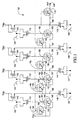
- Pompe à charge comprenant :un corps semiconducteur (202) ayant un type de conductivité particulier,un premier puits (206) dans ledit corps semiconducteur ayant ledit type de conductivité particulier,un deuxième puits (204) dans ledit corps semiconducteur entourant ledit premier puits et ayant un type de conductivité opposé par rapport au type de conductivité particulier,une pluralité de transistors (106 à 110 ; 507 à 512), chacun des transistors dans la pluralité ayant une borne de source et une borne de drain, la pluralité de transistors étant disposés en série d'un premier transistor dans la série relié à une tension d'alimentation (VDD ; GND) à un dernier transistor (110 ; 512) dans la pluralité relié à une sortie de la pompe à charge, pour pomper un niveau de tension de ladite sortie de la pompe à charge en réponse à une ou plusieurs impulsions d'horloge, ledit dernier transistor présentant un niveau de tension sensiblement supérieur à ladite tension d'alimentation pour une sortie de tension positive, ou négative par rapport à celle-ci, pour une sortie de tension négative, la pluralité de transistors dans la série étant connectés de sorte que, pour une sortie de tension positive, la source de l'un des transistors dans la série est connectée au drain d'un transistor précédent dans la série, et pour une sortie de tension négative, le drain de l'un des transistors dans la série est connecté à la source d'un transistor précédent dans la série,caractérisée en ce que
ladite borne de source et ladite borne de drain dudit au moins un transistor de ladite pluralité de transistors comprennent des régions respectives dudit type de conduction opposé formées dans ledit premier puits, ledit premier puits, ledit deuxième puits et ladite région de source étant connectés ensemble. - Pompe à charge selon la revendication 1, dans laquelle ladite tension d'alimentation se trouve dans une plage entre approximativement 5 et approximativement 1,5 volts.
- Pompe à charge selon la revendication 1, dans laquelle ladite tension d'alimentation est sensiblement égale à 3 volts.
- Pompe à charge selon la revendication 1, dans laquelle ladite tension d'alimentation est sensiblement égale à 2 volts.
- Pompe à charge selon la revendication 1, dans laquelle au moins l'une desdites impulsions d'horloge agit à une fréquence au-dessus de 10 MHz.
- Pompe à charge selon la revendication 1, dans laquelle au moins l'une desdites impulsions d'horloge agit à une fréquence approximativement égale à 22 MHz.
- Pompe à charge selon la revendication 1, dans laquelle ledit niveau de tension au niveau dudit dernier transistor est positif.
- Pompe à charge selon la revendication 1, dans laquelle ledit niveau de tension au niveau dudit dernier transistor est négatif.
- Pompe à charge selon la revendication 1, comprenant en outre un moyen destiné à coupler lesdites impulsions d'horloge auxdits transistors.
- Pompe à charge selon la revendication 12, dans laquelle ledit moyen de couplage comprend un transistor MOS.
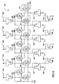
- Pompe à charge selon la revendication 1, dans laquelle ladite pluralité de transistors comprend une pluralité d'étages de pompe à charge disposés en série pour pomper ledit niveau de tension d'un premier étage à un dernier étage en réponse à ladite une ou plusieurs impulsions d'horloge, et dans laquelle
au moins l'un des étages de la pompe à charge comprend un premier transistor comportant une grille, une source et un drain et un deuxième transistor ayant une grille couplée au drain du premier transistor, une source couplée à la source du premier transistor et un drain couplé à la grille du premier transistor, et dans laquelle les drains et les sources respectifs des premier et deuxième transistors se trouvent dans le premier puits, et les sources des premier et deuxième transistors sont couplées au premier puits. - Pompe à charge selon la revendication 11, dans laquelle le premier puits et le deuxième puits sont couplés ensemble aux sources des premier et deuxième transistors.
- Pompe à charge selon la revendication 1, dans laquelle ladite pluralité de transistors comprend une pluralité d'étages de pompe à charge disposés en série pour pomper ledit niveau de tension d'un premier étage à un dernier étage en réponse auxdites une ou plusieurs impulsions d'horloge, et dans laquelle
l'étage de pompe à charge respectif dans la pluralité comprend un premier puits dans ledit corps semiconducteur ayant ledit type de conductivité particulier, un deuxième puits dans ledit corps semiconducteur entourant ledit premier puits et ayant un type de conductivité opposé par rapport au type de conductivité particulier, un premier transistor comportant une grille, une source et un drain et un deuxième transistor ayant une grille couplée au drain du premier transistor, une source couplée à la source du premier transistor, et un drain couplé à la grille du premier transistor, et dans laquelle les drains et les sources respectifs des premier et deuxième transistors se trouvent dans le premier puits, et les sources des premier et deuxième transistors sont couplées au premier puits.
Applications Claiming Priority (1)
| Application Number | Priority Date | Filing Date | Title |
|---|---|---|---|
| PCT/US1996/016317 WO1998016010A1 (fr) | 1996-10-10 | 1996-10-10 | Pompe a charge avec trois puits |
Publications (3)
| Publication Number | Publication Date |
|---|---|
| EP0931379A1 EP0931379A1 (fr) | 1999-07-28 |
| EP0931379A4 EP0931379A4 (fr) | 2000-01-19 |
| EP0931379B1 true EP0931379B1 (fr) | 2008-08-06 |
Family
ID=22255942
Family Applications (1)
| Application Number | Title | Priority Date | Filing Date |
|---|---|---|---|
| EP96939448A Expired - Lifetime EP0931379B1 (fr) | 1996-10-10 | 1996-10-10 | Pompe a charge avec trois puits |
Country Status (5)
| Country | Link |
|---|---|
| EP (1) | EP0931379B1 (fr) |
| JP (1) | JP3415854B2 (fr) |
| DE (1) | DE69637632D1 (fr) |
| HK (1) | HK1021268A1 (fr) |
| WO (1) | WO1998016010A1 (fr) |
Families Citing this family (6)
| Publication number | Priority date | Publication date | Assignee | Title |
|---|---|---|---|---|
| DE59915144D1 (de) * | 1998-09-10 | 2010-05-12 | Infineon Technologies Ag | Ladungspumpenschaltung |
| US6160440A (en) * | 1998-09-25 | 2000-12-12 | Intel Corporation | Scaleable charge pump for use with a low voltage power supply |
| US6441442B1 (en) | 2000-05-30 | 2002-08-27 | Programmable Silicon Solutions | Integrated inductive circuits |
| US6917095B1 (en) | 2000-05-30 | 2005-07-12 | Altera Corporation | Integrated radio frequency circuits |
| EP1160842A3 (fr) * | 2000-05-30 | 2003-09-17 | Programmable Silicon Solutions | Circuits integrés à haute fréquence |
| WO2001093317A1 (fr) * | 2000-05-30 | 2001-12-06 | Programmable Silicon Solutions | Circuits inducteurs integres |
Family Cites Families (5)
| Publication number | Priority date | Publication date | Assignee | Title |
|---|---|---|---|---|
| NL8702734A (nl) * | 1987-11-17 | 1989-06-16 | Philips Nv | Spanningsvermenigvuldigschakeling en gelijkrichtelement. |
| JP2771729B2 (ja) * | 1992-04-16 | 1998-07-02 | 三菱電機株式会社 | チャージポンプ回路 |
| JP3307453B2 (ja) * | 1993-03-18 | 2002-07-24 | ソニー株式会社 | 昇圧回路 |
| JP3282915B2 (ja) * | 1994-03-31 | 2002-05-20 | 富士通株式会社 | Dc/dcコンバータ及びnmosトランジスタのバックゲート電圧の制御方法 |
| US7102422B1 (en) * | 1994-04-20 | 2006-09-05 | Nippon Steel Corporation | Semiconductor booster circuit having cascaded MOS transistors |
-
1996
- 1996-10-10 DE DE69637632T patent/DE69637632D1/de not_active Expired - Lifetime
- 1996-10-10 JP JP51747498A patent/JP3415854B2/ja not_active Expired - Lifetime
- 1996-10-10 WO PCT/US1996/016317 patent/WO1998016010A1/fr active Application Filing
- 1996-10-10 EP EP96939448A patent/EP0931379B1/fr not_active Expired - Lifetime
-
1999
- 1999-12-08 HK HK99105726.2A patent/HK1021268A1/xx not_active IP Right Cessation
Also Published As
| Publication number | Publication date |
|---|---|
| JP3415854B2 (ja) | 2003-06-09 |
| DE69637632D1 (de) | 2008-09-18 |
| EP0931379A1 (fr) | 1999-07-28 |
| WO1998016010A1 (fr) | 1998-04-16 |
| HK1021268A1 (en) | 2000-06-02 |
| EP0931379A4 (fr) | 2000-01-19 |
Similar Documents
| Publication | Publication Date | Title |
|---|---|---|
| US6100557A (en) | Triple well charge pump | |
| US7102422B1 (en) | Semiconductor booster circuit having cascaded MOS transistors | |
| US6914791B1 (en) | High efficiency triple well charge pump circuit | |
| US6878981B2 (en) | Triple-well charge pump stage with no threshold voltage back-bias effect | |
| KR910007403B1 (ko) | 반도체 집적회로 | |
| KR100270926B1 (ko) | 승압회로 | |
| KR100367316B1 (ko) | 승압된백게이트바이어스를갖는승압회로 | |
| JP4026947B2 (ja) | 昇圧回路 | |
| US5986947A (en) | Charge pump circuits having floating wells | |
| US5657271A (en) | Nonvolatile semiconductor memory device in which band to band tunneling current is suppressed | |
| US20030057469A1 (en) | Semiconductor charge pump circuit and nonvolatile semiconductor memory device | |
| JPH0845291A (ja) | 単一低電圧電源を用いてフローティングゲートメモリセルをプログラムする方法および回路 | |
| US5581107A (en) | Nonvolatile semiconductor memory that eases the dielectric strength requirements | |
| US7439795B2 (en) | Charge pump circuit with reduced parasitic capacitance | |
| JPH07154964A (ja) | 低電圧チャージポンプ | |
| US9536575B2 (en) | Power source for memory circuitry | |
| US5723985A (en) | Clocked high voltage switch | |
| EP0931379B1 (fr) | Pompe a charge avec trois puits | |
| EP0772200A1 (fr) | Générateur de tension pour cellules de mémoire morte programmable électriquement | |
| WO1997018588A1 (fr) | Pompes a charge ameliorees utilisant des condensateurs a accumulation | |
| JP2000503840A (ja) | 三重ウエルの電荷ポンプ | |
| JP3354709B2 (ja) | 半導体昇圧回路 | |
| Mohammad et al. | Switched positive/negative charge pump design using standard CMOS transistors | |
| JP3354713B2 (ja) | 半導体昇圧回路 | |
| KR100280456B1 (ko) | 반도체 차지 펌프 회로 |
Legal Events
| Date | Code | Title | Description |
|---|---|---|---|
| PUAI | Public reference made under article 153(3) epc to a published international application that has entered the european phase |
Free format text: ORIGINAL CODE: 0009012 |
|
| 17P | Request for examination filed |
Effective date: 19990414 |
|
| AK | Designated contracting states |
Kind code of ref document: A1 Designated state(s): DE FR GB IT |
|
| A4 | Supplementary search report drawn up and despatched |
Effective date: 19991202 |
|
| AK | Designated contracting states |
Kind code of ref document: A4 Designated state(s): DE FR GB IT |
|
| RIC1 | Information provided on ipc code assigned before grant |
Free format text: 7H 03K 17/56 A, 7H 03K 17/687 B, 7H 03K 17/74 B, 7H 01L 29/788 B, 7H 02M 3/07 B |
|
| RAP1 | Party data changed (applicant data changed or rights of an application transferred) |
Owner name: MACRONIX INTERNATIONAL CO., LTD. |
|
| 17Q | First examination report despatched |
Effective date: 20020722 |
|
| GRAP | Despatch of communication of intention to grant a patent |
Free format text: ORIGINAL CODE: EPIDOSNIGR1 |
|
| GRAS | Grant fee paid |
Free format text: ORIGINAL CODE: EPIDOSNIGR3 |
|
| GRAA | (expected) grant |
Free format text: ORIGINAL CODE: 0009210 |
|
| AK | Designated contracting states |
Kind code of ref document: B1 Designated state(s): DE FR GB IT |
|
| REG | Reference to a national code |
Ref country code: GB Ref legal event code: FG4D |
|
| REF | Corresponds to: |
Ref document number: 69637632 Country of ref document: DE Date of ref document: 20080918 Kind code of ref document: P |
|
| REG | Reference to a national code |
Ref country code: HK Ref legal event code: GR Ref document number: 1021268 Country of ref document: HK |
|
| PLBE | No opposition filed within time limit |
Free format text: ORIGINAL CODE: 0009261 |
|
| STAA | Information on the status of an ep patent application or granted ep patent |
Free format text: STATUS: NO OPPOSITION FILED WITHIN TIME LIMIT |
|
| 26N | No opposition filed |
Effective date: 20090507 |
|
| REG | Reference to a national code |
Ref country code: DE Ref legal event code: R039 Ref document number: 69637632 Country of ref document: DE Ref country code: DE Ref legal event code: R008 Ref document number: 69637632 Country of ref document: DE |
|
| REG | Reference to a national code |
Ref country code: DE Ref legal event code: R097 Ref document number: 69637632 Country of ref document: DE Ref country code: DE Ref legal event code: R040 Ref document number: 69637632 Country of ref document: DE |
|
| REG | Reference to a national code |
Ref country code: DE Ref legal event code: R082 Ref document number: 69637632 Country of ref document: DE Representative=s name: WALLINGER RICKER SCHLOTTER TOSTMANN PATENT- UN, DE |
|
| REG | Reference to a national code |
Ref country code: DE Ref legal event code: R039 Ref document number: 69637632 Country of ref document: DE Effective date: 20141110 |
|
| REG | Reference to a national code |
Ref country code: DE Ref legal event code: R040 Ref document number: 69637632 Country of ref document: DE Effective date: 20150127 |
|
| REG | Reference to a national code |
Ref country code: FR Ref legal event code: PLFP Year of fee payment: 20 |
|
| PGFP | Annual fee paid to national office [announced via postgrant information from national office to epo] |
Ref country code: FR Payment date: 20150908 Year of fee payment: 20 |
|
| PGFP | Annual fee paid to national office [announced via postgrant information from national office to epo] |
Ref country code: GB Payment date: 20151007 Year of fee payment: 20 Ref country code: IT Payment date: 20151026 Year of fee payment: 20 Ref country code: DE Payment date: 20151006 Year of fee payment: 20 |
|
| REG | Reference to a national code |
Ref country code: DE Ref legal event code: R071 Ref document number: 69637632 Country of ref document: DE |
|
| REG | Reference to a national code |
Ref country code: GB Ref legal event code: PE20 Expiry date: 20161009 |
|
| PG25 | Lapsed in a contracting state [announced via postgrant information from national office to epo] |
Ref country code: GB Free format text: LAPSE BECAUSE OF EXPIRATION OF PROTECTION Effective date: 20161009 |