EP0926537B1 - Dispositif d'affichage à cristaux liquides - Google Patents
Dispositif d'affichage à cristaux liquides Download PDFInfo
- Publication number
- EP0926537B1 EP0926537B1 EP98123364A EP98123364A EP0926537B1 EP 0926537 B1 EP0926537 B1 EP 0926537B1 EP 98123364 A EP98123364 A EP 98123364A EP 98123364 A EP98123364 A EP 98123364A EP 0926537 B1 EP0926537 B1 EP 0926537B1
- Authority
- EP
- European Patent Office
- Prior art keywords
- pixel
- liquid crystal
- display device
- wire
- dummy
- Prior art date
- Legal status (The legal status is an assumption and is not a legal conclusion. Google has not performed a legal analysis and makes no representation as to the accuracy of the status listed.)
- Expired - Lifetime
Links
Images


Classifications
-
- G—PHYSICS
- G02—OPTICS
- G02F—OPTICAL DEVICES OR ARRANGEMENTS FOR THE CONTROL OF LIGHT BY MODIFICATION OF THE OPTICAL PROPERTIES OF THE MEDIA OF THE ELEMENTS INVOLVED THEREIN; NON-LINEAR OPTICS; FREQUENCY-CHANGING OF LIGHT; OPTICAL LOGIC ELEMENTS; OPTICAL ANALOGUE/DIGITAL CONVERTERS
- G02F1/00—Devices or arrangements for the control of the intensity, colour, phase, polarisation or direction of light arriving from an independent light source, e.g. switching, gating or modulating; Non-linear optics
- G02F1/01—Devices or arrangements for the control of the intensity, colour, phase, polarisation or direction of light arriving from an independent light source, e.g. switching, gating or modulating; Non-linear optics for the control of the intensity, phase, polarisation or colour
- G02F1/13—Devices or arrangements for the control of the intensity, colour, phase, polarisation or direction of light arriving from an independent light source, e.g. switching, gating or modulating; Non-linear optics for the control of the intensity, phase, polarisation or colour based on liquid crystals, e.g. single liquid crystal display cells
- G02F1/133—Constructional arrangements; Operation of liquid crystal cells; Circuit arrangements
- G02F1/136—Liquid crystal cells structurally associated with a semi-conducting layer or substrate, e.g. cells forming part of an integrated circuit
- G02F1/1362—Active matrix addressed cells
- G02F1/1365—Active matrix addressed cells in which the switching element is a two-electrode device
-
- G—PHYSICS
- G02—OPTICS
- G02F—OPTICAL DEVICES OR ARRANGEMENTS FOR THE CONTROL OF LIGHT BY MODIFICATION OF THE OPTICAL PROPERTIES OF THE MEDIA OF THE ELEMENTS INVOLVED THEREIN; NON-LINEAR OPTICS; FREQUENCY-CHANGING OF LIGHT; OPTICAL LOGIC ELEMENTS; OPTICAL ANALOGUE/DIGITAL CONVERTERS
- G02F1/00—Devices or arrangements for the control of the intensity, colour, phase, polarisation or direction of light arriving from an independent light source, e.g. switching, gating or modulating; Non-linear optics
- G02F1/01—Devices or arrangements for the control of the intensity, colour, phase, polarisation or direction of light arriving from an independent light source, e.g. switching, gating or modulating; Non-linear optics for the control of the intensity, phase, polarisation or colour
- G02F1/13—Devices or arrangements for the control of the intensity, colour, phase, polarisation or direction of light arriving from an independent light source, e.g. switching, gating or modulating; Non-linear optics for the control of the intensity, phase, polarisation or colour based on liquid crystals, e.g. single liquid crystal display cells
- G02F1/133—Constructional arrangements; Operation of liquid crystal cells; Circuit arrangements
- G02F1/136—Liquid crystal cells structurally associated with a semi-conducting layer or substrate, e.g. cells forming part of an integrated circuit
- G02F1/1362—Active matrix addressed cells
- G02F1/136286—Wiring, e.g. gate line, drain line
Landscapes
- Physics & Mathematics (AREA)
- Nonlinear Science (AREA)
- Engineering & Computer Science (AREA)
- Microelectronics & Electronic Packaging (AREA)
- Mathematical Physics (AREA)
- Chemical & Material Sciences (AREA)
- Crystallography & Structural Chemistry (AREA)
- General Physics & Mathematics (AREA)
- Optics & Photonics (AREA)
- Liquid Crystal (AREA)
- Infusion, Injection, And Reservoir Apparatuses (AREA)
Claims (12)
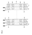
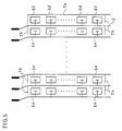
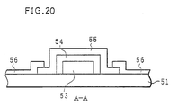
- Dispositif d'affichage à cristaux liquides comprenant une pluralité de pixels, qui forment un écran d'affichage et sont agencés sous forme de matrice, et des fils de signaux (2), dans lequel tous les pixels formant une ligne de pixels respective de ladite matrice sont connectés avec un fil de signaux correspondants (2), ledit dispositif d'affichage comprenant en outre :un premier fil factice (7a) qui est formé le long d'un extérieur d'une ligne de pixels finale avec aucun fil de signaux voisin autre qu'un fil de signaux final (2a) étant connecté avec la ligne de pixels finale, et qui est agencé pour appliquer aux électrodes de pixel (6d à 6f) disposées sur la ligne de pixels finale la même quantité de capacité parasite qu'une capacité parasite interligne qui est appliquée depuis un fil de signaux voisin, dans lequel ledit premier fil factice est connecté électriquement avec le fil de signaux final voisin,caractérisé en ce quele dispositif d'affichage à cristaux liquides comprend en outre des deuxièmes fils factices (7b) qui sont formés sur l'extérieur respectif des pixels disposés sur les deux extrémités des lignes de pixels, chaque deuxième fil factice étant connecté avec un fil de signaux respectif, et étant agencé pour appliquer aux électrodes de pixel (6e à 6f) des pixels disposés sur les deux extrémités la même quantité de capacité parasite qu'une capacité parasite interpixel qui est appliquée depuis l'électrode de pixel voisine dans la ligne de pixels.
- Dispositif d'affichage à cristaux liquides comprenant une pluralité de pixels, qui forment un écran d'affichage et sont agencés sous forme de matrice et des fils de signaux (2), dans lequel tous les pixels formant une ligne de pixels respective de ladite matrice sont connectés avec un fil de signaux correspondant (2), ledit dispositif d'affichage comprenant en outre :un premier fil factice (7a) qui est formé le long d'un extérieur d'une ligne de pixels finale avec aucun fil de signaux voisin autre qu'un fil de signaux final (2a) étant connecté avec la ligne de pixels finale, et qui est agencé pour appliquer aux électrodes de pixel (6d à 6f) disposées sur la ligne de pixels finale la même quantité de capacité parasite qu'une capacité parasite interligne qui est appliquée depuis le fil de signaux voisin,caractérisé en ce quele dispositif d'affichage à cristaux liquides comprend en outre une électrode de balayage transparente (8) qui est formée sur un substrat transparent à l'opposé d'un substrat sur lequel ledit premier fil factice (7a) est formé, ledit premier fil factice étant connecté électriquement avec aucun des fils de signaux, mais étant chargé électriquement du fait d'un effet électrique de l'électrode de balayage transparente, et les deuxièmes fils factices (7b) qui sont formés sur l'extérieur respectif des pixels disposés sur les deux extrémités des lignes de pixels, chaque deuxième fil factice étant connecté avec un fil de signaux respectif, et étant agencé pour appliquer aux électrodes de pixel (6e à 6f) des pixels disposés sur les deux extrémités la même quantité de capacité parasite qu'une capacité parasite interpixel qui est appliquée depuis l'électrode de pixel voisine dans la ligne de pixels.
- Dispositif d'affichage à cristaux liquides selon la revendication 1 ou 2, dans lequel un deuxième fil factice respectif (7b) s'étend depuis le fil de signaux (2a) qui est connecté à l'électrode de pixel, à laquelle ledit deuxième fil factice applique la capacité parasite.
- Dispositif d'affichage à cristaux liquides selon la revendication 1 ou 2, dans lequel un deuxième fil factice respectif (7b) s'étend d'un fil de signaux (2b) qui n'est pas connecté à l'électrode de pixel, à laquelle ledit deuxième fil factice applique la capacité parasite.
- Dispositif d'affichage à cristaux liquides selon l'une quelconque des revendications 1 à 4, comprenant en outre des troisièmes fils factices (7c) qui sont disposés entre des électrodes de pixel voisines dans les lignes de pixels, les troisièmes fils factices étant connectés avec un fil de signaux respectif (2) de façon à appliquer une capacité parasite égale à l'électrode de pixel voisine.
- Dispositif d'affichage à cristaux liquides selon la revendication 5, dans lequel un troisième fil factice respectif (7c) s'étend depuis le fil de signaux (2a) qui est connecté à l'électrode de pixel, à laquelle ledit troisième fil factice applique la capacité parasite.
- Dispositif d'affichage à cristaux liquides selon la revendication 5, dans lequel un troisième fil factice respectif (7c) s'étend depuis un fil de signaux (2b) qui n'est pas connecté avec l'électrode de pixel, à laquelle le troisième fil factice applique la capacité parasite.
- Dispositif d'affichage à cristaux liquides selon l'une quelconque des revendications 1 à 7, dans lequel lesdits fils de signaux (2) sont divisés à un centre et agencés de telle sorte qu'un signal peut être fourni en entrée à chaque fil de signaux depuis les deux extrémités des fils de signaux.
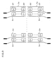
- Dispositif d'affichage à cristaux liquides selon l'une quelconque des revendications 5 à 7, dans lequel les premiers, deuxièmes et troisièmes fils factices sont agencés de sorte que chacune des électrodes de pixel constituant ledit panneau d'affichage est entourée par un fil factice (7d) ayant une forme identique.
- Dispositif d'affichage à cristaux liquides selon l'une quelconque des revendications 1 à 9, dans lequel chacun desdits pixels comprend un élément métal-isolant-métal MIM qui est connecté avec l'électrode de pixel en série, en tant qu'élément de commutation.
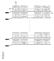
- Dispositif d'affichage à cristaux liquides selon l'une quelconque des revendications 1 à 10, caractérisé en ce qu'un intervalle entre des électrodes de pixel sur chaque ligne de pixels ainsi qu'un intervalle entre l'électrode de pixel disposée sur chaque ligne de pixel et le fil de signaux qui est adjacent à l'électrode de pixel sont étendus de sorte que, par rapport aux capacités parasites qui ne sont pas ajoutées par les fils factices, mais qui consistent en la capacité parasite interligne et la capacité parasite interpixel, chaque capacité parasite appliquée à chaque électrode de pixel n'est pas supérieure à 5 % par rapport à la capacité de l'élément d'électrode.
- Dispositif d'affichage à cristaux liquides selon l'une quelconque des revendications 1 à 11, dans lequel la capacité parasite interligne et la capacité parasite interpixel sont agencées de façon à être uniformes pour chaque électrode de pixel.
Applications Claiming Priority (2)
| Application Number | Priority Date | Filing Date | Title |
|---|---|---|---|
| JP36124597 | 1997-12-26 | ||
| JP36124597A JP3335895B2 (ja) | 1997-12-26 | 1997-12-26 | 液晶表示装置 |
Publications (3)
| Publication Number | Publication Date |
|---|---|
| EP0926537A2 EP0926537A2 (fr) | 1999-06-30 |
| EP0926537A3 EP0926537A3 (fr) | 1999-07-14 |
| EP0926537B1 true EP0926537B1 (fr) | 2012-05-09 |
Family
ID=18472793
Family Applications (1)
| Application Number | Title | Priority Date | Filing Date |
|---|---|---|---|
| EP98123364A Expired - Lifetime EP0926537B1 (fr) | 1997-12-26 | 1998-12-08 | Dispositif d'affichage à cristaux liquides |
Country Status (3)
| Country | Link |
|---|---|
| US (2) | US6333771B1 (fr) |
| EP (1) | EP0926537B1 (fr) |
| JP (1) | JP3335895B2 (fr) |
Families Citing this family (16)
| Publication number | Priority date | Publication date | Assignee | Title |
|---|---|---|---|---|
| KR20020052137A (ko) * | 2000-12-23 | 2002-07-02 | 구본준, 론 위라하디락사 | 액정표시장치 |
| KR100394026B1 (ko) * | 2000-12-27 | 2003-08-06 | 엘지.필립스 엘시디 주식회사 | 액정표시장치 및 그 구동방법 |
| JP2002244585A (ja) * | 2001-02-02 | 2002-08-30 | Koninkl Philips Electronics Nv | 画像表示装置 |
| US20030016318A1 (en) * | 2001-07-23 | 2003-01-23 | Wei-Chen Liang | Color display |
| JP3730161B2 (ja) | 2001-11-28 | 2005-12-21 | シャープ株式会社 | 液晶表示装置 |
| JP3666662B2 (ja) * | 2002-12-13 | 2005-06-29 | シャープ株式会社 | 表示装置 |
| CN1300753C (zh) * | 2003-02-10 | 2007-02-14 | 三洋电机株式会社 | 动态矩阵型显示装置 |
| TWI274316B (en) * | 2003-12-15 | 2007-02-21 | Tpo Displays Corp | Display circuitry of display panel |
| JP4184334B2 (ja) * | 2003-12-17 | 2008-11-19 | シャープ株式会社 | 表示装置の駆動方法、表示装置、およびプログラム |
| KR100635061B1 (ko) * | 2004-03-09 | 2006-10-17 | 삼성에스디아이 주식회사 | 평판 표시 장치 및 그의 제조 방법 |
| JP2005257929A (ja) * | 2004-03-10 | 2005-09-22 | Sanyo Electric Co Ltd | アクティブマトリクス型表示装置 |
| JP2007184125A (ja) * | 2006-01-05 | 2007-07-19 | Seiko Epson Corp | 発光装置および画像印刷装置 |
| US9285909B2 (en) | 2010-04-09 | 2016-03-15 | Apple Inc. | Equalizing parasitic capacitance effects in touch screens |
| JP5639819B2 (ja) * | 2010-08-30 | 2014-12-10 | 株式会社ジャパンディスプレイ | 表示装置 |
| US9329738B2 (en) * | 2012-09-10 | 2016-05-03 | Apple Inc. | Determination and reduction of parasitic capacitance variation due to display noise |
| KR102058855B1 (ko) * | 2013-12-31 | 2019-12-26 | 엘지디스플레이 주식회사 | 표시장치 |
Citations (2)
| Publication number | Priority date | Publication date | Assignee | Title |
|---|---|---|---|---|
| JPH0572557A (ja) * | 1991-09-17 | 1993-03-26 | Hitachi Ltd | 液晶マトリクス表示装置 |
| JPH0713177A (ja) * | 1993-06-28 | 1995-01-17 | Toshiba Corp | 液晶表示装置 |
Family Cites Families (25)
| Publication number | Priority date | Publication date | Assignee | Title |
|---|---|---|---|---|
| US5177743A (en) * | 1982-02-15 | 1993-01-05 | Hitachi, Ltd. | Semiconductor memory |
| JPS61140982A (ja) | 1984-12-12 | 1986-06-28 | シャープ株式会社 | 液晶表示装置 |
| JPS624724U (fr) | 1985-06-03 | 1987-01-12 | ||
| DE3523206A1 (de) | 1985-06-28 | 1987-01-02 | Bayer Ag | Verfahren zur herstellung von poly(diorganosiloxanen) mit alkoxyendgruppen |
| JPS6258226A (ja) | 1985-09-09 | 1987-03-13 | Seiko Epson Corp | 液晶表示体 |
| JPS643630A (en) | 1987-06-26 | 1989-01-09 | Seiko Instr & Electronics | Electro-optic device |
| JP2590992B2 (ja) | 1987-07-02 | 1997-03-19 | セイコーエプソン株式会社 | 液晶装置及びその駆動方法 |
| JPH01133032A (ja) | 1987-11-18 | 1989-05-25 | Seiko Instr & Electron Ltd | 電気光学装置 |
| JPH027024A (ja) | 1988-06-27 | 1990-01-11 | Fujitsu Ltd | 薄膜トランジスタマトリクス |
| JP2508301B2 (ja) * | 1989-10-23 | 1996-06-19 | 日本電気株式会社 | 半導体集積回路 |
| JPH0473951A (ja) * | 1990-07-16 | 1992-03-09 | Nec Ic Microcomput Syst Ltd | 半導体装置 |
| KR960014823B1 (ko) * | 1991-03-15 | 1996-10-21 | 가부시기가이샤 히다찌세이사구쇼 | 액정표시장치 |
| JPH0527268A (ja) | 1991-07-23 | 1993-02-05 | Toshiba Corp | 液晶表示装置 |
| JPH05249478A (ja) * | 1991-12-25 | 1993-09-28 | Toshiba Corp | 液晶表示装置 |
| JPH0728096A (ja) | 1993-07-14 | 1995-01-31 | Toshiba Corp | 液晶表示装置及びその製造方法 |
| JP3322948B2 (ja) * | 1993-09-17 | 2002-09-09 | 株式会社東芝 | 表示装置用アレイ基板及び液晶表示装置 |
| TW373094B (en) * | 1994-11-14 | 1999-11-01 | Hitachi Device Engineering Corp | Liquid crystal display device having a uniform liquid crystal layer thickness |
| US6169530B1 (en) * | 1995-04-20 | 2001-01-02 | Canon Kabushiki Kaisha | Display apparatus and assembly of its driving circuit |
| TW406204B (en) * | 1995-09-21 | 2000-09-21 | Advanced Display Kk | Liquid crystal display apparatus |
| JP3412390B2 (ja) * | 1996-03-18 | 2003-06-03 | 株式会社ニコン | 光電変換装置 |
| JP3256730B2 (ja) | 1996-04-22 | 2002-02-12 | シャープ株式会社 | 液晶表示装置、およびその駆動方法 |
| US6014191A (en) * | 1996-07-16 | 2000-01-11 | Samsung Electronics Co., Ltd. | Liquid crystal display having repair lines that cross data lines twice and cross gate lines in the active area and related repairing methods |
| US5982470A (en) * | 1996-08-29 | 1999-11-09 | Sharp Kabushiki Kaisha | Liquid crystal display device having dummy electrodes with interleave ratio same on all sides |
| KR100228282B1 (ko) * | 1996-09-17 | 1999-11-01 | 윤종용 | 액정 표시 장치 |
| KR100260611B1 (ko) * | 1997-04-03 | 2000-07-01 | 윤종용 | 배선을 수리하기 위한 평판 표시 장치용 기판 |
-
1997
- 1997-12-26 JP JP36124597A patent/JP3335895B2/ja not_active Expired - Fee Related
-
1998
- 1998-12-08 EP EP98123364A patent/EP0926537B1/fr not_active Expired - Lifetime
- 1998-12-08 US US09/207,403 patent/US6333771B1/en not_active Expired - Lifetime
-
2001
- 2001-11-30 US US09/996,936 patent/US6608655B2/en not_active Expired - Fee Related
Patent Citations (2)
| Publication number | Priority date | Publication date | Assignee | Title |
|---|---|---|---|---|
| JPH0572557A (ja) * | 1991-09-17 | 1993-03-26 | Hitachi Ltd | 液晶マトリクス表示装置 |
| JPH0713177A (ja) * | 1993-06-28 | 1995-01-17 | Toshiba Corp | 液晶表示装置 |
Also Published As
| Publication number | Publication date |
|---|---|
| US20020033924A1 (en) | 2002-03-21 |
| EP0926537A2 (fr) | 1999-06-30 |
| EP0926537A3 (fr) | 1999-07-14 |
| JPH11194370A (ja) | 1999-07-21 |
| US6333771B1 (en) | 2001-12-25 |
| US6608655B2 (en) | 2003-08-19 |
| JP3335895B2 (ja) | 2002-10-21 |
Similar Documents
| Publication | Publication Date | Title |
|---|---|---|
| EP0926537B1 (fr) | Dispositif d'affichage à cristaux liquides | |
| KR100361626B1 (ko) | 액티브 매트릭스형 액정표시장치 | |
| EP0399846B1 (fr) | Dispositif d'affichage à matrice active et son procédé de fabrication | |
| US6226057B1 (en) | Liquid crystal display having overlapped pixel electrodes and method for fabricating the same | |
| US5870163A (en) | LCD device with connection lines having different resistances | |
| JPH10142633A (ja) | 薄膜トランジスタ集積装置およびその製造方法並びに液晶表示装置 | |
| KR19980028450A (ko) | 평면 구동 방식의 액정 표시 장치 | |
| US5847684A (en) | Display device with mirror-symmetrical pixels | |
| EP0605176B1 (fr) | Panneau d'affichage à cristal liquide et son procédé de fabrication | |
| US20030122976A1 (en) | Liquid crystal display having shorting bar for testing thin film transistor | |
| US7876388B2 (en) | Array substrate capable of improving display quality | |
| JP3636192B2 (ja) | 液晶装置及び電子機器 | |
| JP3209652B2 (ja) | 液晶表示装置 | |
| US6888603B2 (en) | IPS-LCD with a compensation structure for reducing transmittance difference | |
| JPH0827465B2 (ja) | 平面デイスプレイ | |
| JP3092747B2 (ja) | アクティブマトリクス表示装置 | |
| US5568289A (en) | Liquid crystal display device | |
| KR100361624B1 (ko) | 액정표시장치 | |
| JP2775892B2 (ja) | 2端子素子型液晶表示装置 | |
| JP3380857B2 (ja) | 液晶表示装置 | |
| JP2551343B2 (ja) | 液晶表示装置 | |
| JP3480682B2 (ja) | 液晶表示装置 | |
| JP2526949Y2 (ja) | マトリクス形液晶表示装置 | |
| JP2692685B2 (ja) | 液晶パネル | |
| JP3380856B2 (ja) | 液晶表示装置 |
Legal Events
| Date | Code | Title | Description |
|---|---|---|---|
| PUAI | Public reference made under article 153(3) epc to a published international application that has entered the european phase |
Free format text: ORIGINAL CODE: 0009012 |
|
| PUAL | Search report despatched |
Free format text: ORIGINAL CODE: 0009013 |
|
| AK | Designated contracting states |
Kind code of ref document: A2 Designated state(s): DE GB |
|
| AX | Request for extension of the european patent |
Free format text: AL;LT;LV;MK;RO;SI |
|
| AK | Designated contracting states |
Kind code of ref document: A3 Designated state(s): AT BE CH CY DE DK ES FI FR GB GR IE IT LI LU MC NL PT SE |
|
| AX | Request for extension of the european patent |
Free format text: AL;LT;LV;MK;RO;SI |
|
| 17P | Request for examination filed |
Effective date: 19991014 |
|
| AKX | Designation fees paid |
Free format text: DE GB |
|
| 17Q | First examination report despatched |
Effective date: 20060328 |
|
| REG | Reference to a national code |
Ref country code: DE Ref legal event code: R079 Ref document number: 69842713 Country of ref document: DE Free format text: PREVIOUS MAIN CLASS: G02F0001134300 Ipc: G02F0001136200 |
|
| GRAP | Despatch of communication of intention to grant a patent |
Free format text: ORIGINAL CODE: EPIDOSNIGR1 |
|
| GRAJ | Information related to disapproval of communication of intention to grant by the applicant or resumption of examination proceedings by the epo deleted |
Free format text: ORIGINAL CODE: EPIDOSDIGR1 |
|
| GRAC | Information related to communication of intention to grant a patent modified |
Free format text: ORIGINAL CODE: EPIDOSCIGR1 |
|
| GRAP | Despatch of communication of intention to grant a patent |
Free format text: ORIGINAL CODE: EPIDOSNIGR1 |
|
| RIC1 | Information provided on ipc code assigned before grant |
Ipc: G02F 1/1365 20060101ALI20111130BHEP Ipc: G02F 1/1362 20060101AFI20111130BHEP |
|
| GRAS | Grant fee paid |
Free format text: ORIGINAL CODE: EPIDOSNIGR3 |
|
| GRAA | (expected) grant |
Free format text: ORIGINAL CODE: 0009210 |
|
| AK | Designated contracting states |
Kind code of ref document: B1 Designated state(s): DE GB |
|
| REG | Reference to a national code |
Ref country code: GB Ref legal event code: FG4D |
|
| REG | Reference to a national code |
Ref country code: DE Ref legal event code: R096 Ref document number: 69842713 Country of ref document: DE Effective date: 20120628 |
|
| PGFP | Annual fee paid to national office [announced via postgrant information from national office to epo] |
Ref country code: GB Payment date: 20121205 Year of fee payment: 15 |
|
| PLBE | No opposition filed within time limit |
Free format text: ORIGINAL CODE: 0009261 |
|
| STAA | Information on the status of an ep patent application or granted ep patent |
Free format text: STATUS: NO OPPOSITION FILED WITHIN TIME LIMIT |
|
| 26N | No opposition filed |
Effective date: 20130212 |
|
| PGFP | Annual fee paid to national office [announced via postgrant information from national office to epo] |
Ref country code: DE Payment date: 20121219 Year of fee payment: 15 |
|
| REG | Reference to a national code |
Ref country code: DE Ref legal event code: R097 Ref document number: 69842713 Country of ref document: DE Effective date: 20130212 |
|
| REG | Reference to a national code |
Ref country code: DE Ref legal event code: R119 Ref document number: 69842713 Country of ref document: DE |
|
| GBPC | Gb: european patent ceased through non-payment of renewal fee |
Effective date: 20131208 |
|
| REG | Reference to a national code |
Ref country code: DE Ref legal event code: R119 Ref document number: 69842713 Country of ref document: DE Effective date: 20140701 |
|
| PG25 | Lapsed in a contracting state [announced via postgrant information from national office to epo] |
Ref country code: DE Free format text: LAPSE BECAUSE OF NON-PAYMENT OF DUE FEES Effective date: 20140701 |
|
| PG25 | Lapsed in a contracting state [announced via postgrant information from national office to epo] |
Ref country code: GB Free format text: LAPSE BECAUSE OF NON-PAYMENT OF DUE FEES Effective date: 20131208 |