EP0926537B1 - Liquid crystal display device - Google Patents
Liquid crystal display device Download PDFInfo
- Publication number
- EP0926537B1 EP0926537B1 EP98123364A EP98123364A EP0926537B1 EP 0926537 B1 EP0926537 B1 EP 0926537B1 EP 98123364 A EP98123364 A EP 98123364A EP 98123364 A EP98123364 A EP 98123364A EP 0926537 B1 EP0926537 B1 EP 0926537B1
- Authority
- EP
- European Patent Office
- Prior art keywords
- pixel
- liquid crystal
- display device
- wire
- dummy
- Prior art date
- Legal status (The legal status is an assumption and is not a legal conclusion. Google has not performed a legal analysis and makes no representation as to the accuracy of the status listed.)
- Expired - Lifetime
Links
Images


Classifications
-
- G—PHYSICS
- G02—OPTICS
- G02F—OPTICAL DEVICES OR ARRANGEMENTS FOR THE CONTROL OF LIGHT BY MODIFICATION OF THE OPTICAL PROPERTIES OF THE MEDIA OF THE ELEMENTS INVOLVED THEREIN; NON-LINEAR OPTICS; FREQUENCY-CHANGING OF LIGHT; OPTICAL LOGIC ELEMENTS; OPTICAL ANALOGUE/DIGITAL CONVERTERS
- G02F1/00—Devices or arrangements for the control of the intensity, colour, phase, polarisation or direction of light arriving from an independent light source, e.g. switching, gating or modulating; Non-linear optics
- G02F1/01—Devices or arrangements for the control of the intensity, colour, phase, polarisation or direction of light arriving from an independent light source, e.g. switching, gating or modulating; Non-linear optics for the control of the intensity, phase, polarisation or colour
- G02F1/13—Devices or arrangements for the control of the intensity, colour, phase, polarisation or direction of light arriving from an independent light source, e.g. switching, gating or modulating; Non-linear optics for the control of the intensity, phase, polarisation or colour based on liquid crystals, e.g. single liquid crystal display cells
- G02F1/133—Constructional arrangements; Operation of liquid crystal cells; Circuit arrangements
- G02F1/136—Liquid crystal cells structurally associated with a semi-conducting layer or substrate, e.g. cells forming part of an integrated circuit
- G02F1/1362—Active matrix addressed cells
- G02F1/1365—Active matrix addressed cells in which the switching element is a two-electrode device
-
- G—PHYSICS
- G02—OPTICS
- G02F—OPTICAL DEVICES OR ARRANGEMENTS FOR THE CONTROL OF LIGHT BY MODIFICATION OF THE OPTICAL PROPERTIES OF THE MEDIA OF THE ELEMENTS INVOLVED THEREIN; NON-LINEAR OPTICS; FREQUENCY-CHANGING OF LIGHT; OPTICAL LOGIC ELEMENTS; OPTICAL ANALOGUE/DIGITAL CONVERTERS
- G02F1/00—Devices or arrangements for the control of the intensity, colour, phase, polarisation or direction of light arriving from an independent light source, e.g. switching, gating or modulating; Non-linear optics
- G02F1/01—Devices or arrangements for the control of the intensity, colour, phase, polarisation or direction of light arriving from an independent light source, e.g. switching, gating or modulating; Non-linear optics for the control of the intensity, phase, polarisation or colour
- G02F1/13—Devices or arrangements for the control of the intensity, colour, phase, polarisation or direction of light arriving from an independent light source, e.g. switching, gating or modulating; Non-linear optics for the control of the intensity, phase, polarisation or colour based on liquid crystals, e.g. single liquid crystal display cells
- G02F1/133—Constructional arrangements; Operation of liquid crystal cells; Circuit arrangements
- G02F1/136—Liquid crystal cells structurally associated with a semi-conducting layer or substrate, e.g. cells forming part of an integrated circuit
- G02F1/1362—Active matrix addressed cells
- G02F1/136286—Wiring, e.g. gate line, drain line
Landscapes
- Physics & Mathematics (AREA)
- Nonlinear Science (AREA)
- Engineering & Computer Science (AREA)
- Microelectronics & Electronic Packaging (AREA)
- Mathematical Physics (AREA)
- Chemical & Material Sciences (AREA)
- Crystallography & Structural Chemistry (AREA)
- General Physics & Mathematics (AREA)
- Optics & Photonics (AREA)
- Liquid Crystal (AREA)
- Infusion, Injection, And Reservoir Apparatuses (AREA)
Description
- The present invention relates to a liquid crystal display device, and particularly concerns a liquid crystal display device which provides a display by a matrix driving system.
- In recent years, a liquid crystal display device has been widely used for providing a display of a personal computer, a word processor, a terminal display device for office automation, and a television and others thanks to its low power consumption, thin structure, and light weight; accordingly, a display with a larger capacity and higher picture quality has been demanded.
- A conventional liquid crystal display device has performed a simple-matrix driving in accordance with a voltage averaging method of the STN(Super Twisted Nematic) system; however, since a sufficient contrast ratio cannot be obtained due to the increase of scanning lines, this method is not suitable for a display with a large capacity. Therefore, an active-matrix driving has been developed to provide a switching element on each of the pixels constituting a display screen.
- As the aforementioned switching element, a thin-film transistor and a two-terminal nonlinear element are used, and the liquid crystal display device with the two-terminal nonlinear element has been highly evaluated because of the simple construction and low manufacturing cost. A device having a structure of metal-insulator-metal (hereinafter, referred to as MIM) has been put into practical use. For example, a conventional MIM element is produced as follows:
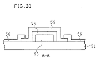
- Firstly, as shown in
Figs. 19 and20 , on aglass substrate 51, a tantalum thin-film, which is formed to be asignal wire 52 and alower electrode 53, is laminated with a thickness of 3000Å in accordance with a sputtering method, etc., and is patterned into a predetermined form so as to obtain thesignal wire 52 and thelower electrode 53 by a photolithography method. Thereafter, in accordance with an anodic oxidation method, an anodic oxidation is performed on the surface of thelower electrode 53 so that aninsulating film 54 is formed with a thickness of 600Å. - And then, in this state, titanium formed to be an
upper electrode 55 is laminated on the entire area of the substrate with a thickness of 4000Å by the sputtering method, etc., and is patterned into a predetermined form by the photolithography method so as to be formed as theupper electrode 55. - Further, a transparent electrode film which is made of ITO and others is laminated on the substrate, and the substrate is subjected to patterning so as to form a
pixel electrode 56.Fig. 21 illustrates an arrangement pattern of pixels composed of MIM elements andpixel electrodes 56, said MIM elements andpixel electrodes 56 being formed in accordance with the aforementioned process. - As described in
Fig. 21 , in the liquid crystal display device which uses the matrix driving system, a parasitic capacity appears in each pixel due to the effects of neighboring pixels and wires. Further, in addition to the case of the aforementioned liquid crystal display device which uses a two-terminal element such as an MIM element and others, the parasitic capacity appears to some extent even in the case of a liquid crystal display device using other active elements or in the case of a liquid crystal display device using the simple-matrix driving system. Especially, in the case of the liquid crystal display device which uses the two-terminal elements, the effect of the parasitic capacity becomes the greatest. - That is, in the case of the liquid crystal display device using the two-terminal element as a switching element, when an element capacity varies in accordance with a change in element dimensions and others of the two-terminal element, a threshold voltage Vth varies accordingly; therefore, a lighting condition differs between pixels. Consequently, with regard to all pixels, it is significant to obtain uniform capacity ratios of a pixel capacity and the element capacity. The pixel capacity is a capacity of the
pixel electrode 56, and the element capacity is a capacity of the MIM element. Here, the parasitic capacity greatly influences the capacity ratio. - The specific explanation will be given in accordance with
Fig. 21 . Based upon one pixel(sample pixel) among a plurality of pixels which are arranged in a matrix form,signal wires pixel electrode 56a of the sample pixel. Further, apixel electrode 56b of a pixel which exists above the sample pixel adds a parasitic capacity C3, and apixel electrode 56c of a pixel which exists below the sample pixel adds a parasitic capacity C4. - The parasitic capacities C1 through C4 are added to the pixel capacity of the
pixel electrode 56a, thereby having an effect on the capacity ratio of the pixel capacity and the element capacity. Namely, with regard to the respective pixels, even if element dimensions of the two-terminal element are arranged so as to be uniform in order to keep the element capacity at a certain amount, the capacity ratio of the pixel capacity and the element capacity varies in accordance with a change in the parasitic capacity. - However, in the conventional arrangement, as shown in
Fig. 22 ,pixel electrodes 56d, which exist on the right end, do not have thesignal wire 52 on its right; therefore, the parasitic capacity C2 is not added. Further,pixel electrodes 56e, which exist on the upper end or the lower end, do not have thepixel electrodes 56 above or below; thus, the parasitic capacity C3 or C4 is not added. Moreover, in the case ofpixel electrodes 56f, which exist on the upper right corner or the lower right corner, parasitic capacities C2 and C3 are not added, or parasitic capacities C2 and C4 are not added. - Hence, with regard to the liquid crystal display device which uses the aforementioned MIM element, each of the parasitic capacities which are applied to the
pixel electrodes pixel 56a, illustrated inFig. 21 . Consequently, since a lighting condition differs between pixels, it becomes impossible to provide an even lighting display. - Namely, as illustrated in
Fig. 22 , with regard to pixels which exist on the upper end, lower end, and on the right end(pixels indicated by slanting lines inFig. 22 ), the threshold voltage Vth becomes lower, resulting in an uneven display. Therefore, for example, in the case of a gradation display, this arrangement causes adverse effects. - From
JP 05 072557 A claims - With regard to a liquid crystal display device with the matrix driving system, the objective of the present invention is to provide a liquid crystal display device which is capable of reducing the influence caused by a difference in parasitic capacity so as to provide an even display.
- In order to achieve the aforementioned objective, the liquid crystal display device of the present invention is as defined in
claims - For a fuller understanding of the nature and advantages of the invention, reference should be made to the ensuing detailed description taken in conjunction with the accompanying drawings.
-
-
Fig. 1 is an explanatory drawing which shows an embodiment of the present invention and a pattern formation of pixels and wires in a liquid crystal display device. -
Fig. 2 is a top view showing the construction of a pixel which uses a two-terminal element as a switching element in the liquid crystal display device. -
Fig. 3 is an A-A cross section showing the pixel. -
Fig. 4 is an explanatory drawing showing parasitic capacities applied to a sample pixel. -
Fig. 5 is an explanatory drawing showing another embodiment of the present invention and a pattern formation of pixels and wires in the liquid crystal display device. -
Fig. 6 is an explanatory drawing showing still another embodiment of the present invention and a pattern formation of pixels and wires in the liquid crystal display device. -
Fig. 7 is an explanatory drawing showing still another embodiment of the present invention and a pattern formation of pixels and wires in the liquid crystal display device. -
Fig. 8 is an explanatory drawing showing still another embodiment of the present invention and a pattern formation of pixels and wires in the liquid crystal display device. -
Fig. 9 is an explanatory drawing showing still another embodiment of the present invention and a pattern formation of pixels and wires in the liquid crystal display device. -
Fig. 10 is an explanatory drawing showing a comparative example of the construction ofFig. 9 and a pattern formation of pixels and wires in the liquid crystal display device. -
Fig. 11 is an explanatory drawing showing still another embodiment of the present invention and a pattern formation of pixels and wires in the liquid crystal display device. -
Fig. 12 is an explanatory drawing showing another pattern formation of pixels and wires in a liquid crystal display device not according to the invention. -
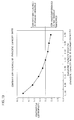
Fig. 13 is a graph which shows the relationship between a parasitic capacity ratio and a contrast difference. -
Fig. 14 is an explanatory drawing showing another pattern formation of pixels and wires in a liquid crystal display device not according to the invention. -
Fig. 15 is an explanatory drawing showing another pattern formation of pixels and wires in a liquid crystal display device not according to the invention. -
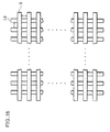
Fig. 16 is an explanatory drawing showing a pattern formation of electrodes in a conventional liquid crystal display device with a simple-matrix system. -
Fig. 17 is an explanatory drawing showing another pattern formation of electrodes in a liquid crystal display device with the simple-matrix system not according to the invention. -
Fig. 18 is an explanatory drawing showing another pattern formation of electrodes in a liquid crystal display device with the simple-matrix system not according to the invention. -
Fig. 19 is a top view showing the construction of a pixel which uses the two-terminal element as a switching element. -
Fig. 20 is an A-A cross section of the pixel. -
Fig. 21 is an explanatory drawing showing parasitic capacities applied to a sample pixel. -
Fig. 22 is an explanatory drawing showing a pattern formation of electrodes in the conventional liquid crystal display device. - Referring to
Figs. 1 through 9 , the following explanation describes one embodiment of the present invention. - The liquid crystal display device of the present embodiment is provided with a liquid crystal panel whose pixels are arranged in a matrix form. Here, as an example, this embodiment exemplifies a case wherein each pixel of the liquid crystal panel uses a two-terminal element such as an MIM element shown in
Figs. 2 and3 as a switching element. - As shown in
Figs. 2 and3 , asignal wire 2 and alower electrode 3, which are obtained by allowing a tantalum thin film to be patterned into a predetermined form on aglass substrate 1, are formed in the aforementioned pixel. Further, an insulating film 4 is formed on the surface of thelower electrode 3 in accordance with an anodic oxidation method. - An
upper electrode 5, which is obtained by allowing a titanium thin film to be patterned into a predetermined form, is formed on thelower electrode 3. Apixel electrode 6, which is obtained by allowing a transparent film made of ITO and others to be patterned, is formed on theupper electrode 5. - As described above, in the case of the liquid crystal display device which is provided with the liquid crystal panel whose pixels are arranged in a matrix form, a parasitic capacity appears due to the influence of pixels and wires which are adjacent to each pixel. If the parasitic capacity differs between pixels, it becomes impossible to achieve a uniform image display, as mentioned in Prior Art.
- Furthermore, based upon one pixel(sample pixel) of the liquid crystal panel, the present embodiment defines the arrangement of pixels and wires which are adjacent to the sample pixel as follows. Here, the sample pixel is not supposed to belong to any lines disposed on the upper end, the lower end, and the right end of the liquid crystal panel.
- As described in
Fig. 4 , apixel electrode 6a represents the pixel electrode of the sample pixel, apixel electrode 6b represents a pixel electrode of a pixel which is disposed above the sample pixel, and a pixel electrode 6c represents a pixel electrode of a pixel which is disposed below the sample pixel. Moreover, among two signal wires which are adjacent to the sample pixel, asignal wire 2a represents a signal wire which is connected with the sample pixel, and a signal wire 2b represents the other signal wire which is not connected with the sample pixel. - As described above, with regard to the
pixel electrode 6a of the pixel which is surrounded by other pixels and signal wires from all directions, thesignal wires 2a and 2b add parasitic capacities C1 and C2 serving as between-line parasitic capacities, and thepixel electrodes 6b and 6c add parasitic capacities C3 and C4 serving as between-pixels parasitic capacities. Namely, with regard to thepixel electrode 6a, four kinds of parasitic capacities, that is, the parasitic capacities C1 through C4 appear. - By contrast, with regard to pixels which are disposed on the upper end, the lower end, and the right end, as described in Prior Art, only two or three kinds of the aforementioned four parasitic capacities C1 through C4 appear. This causes an uneven lighting display as shown in
Fig. 22 . - In order to improve the uneven lighting display, the liquid crystal display device of the present embodiment is, as shown in
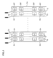
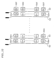
Fig. 1 , provided withdummy wires - The
dummy wire 7a is installed for providing the pixel which is disposed on the right end with a parasitic capacity corresponding to the parasitic capacity C2, and is formed on the right of the right end, in parallel with thesignal wire 2. Further, thedummy wire 7b is installed for providing a pixel which is disposed on the upper end or the lower end with a parasitic capacity corresponding to the parasitic capacity C3 or C4. Thedummy wire 7b, located above the upper end or below the lower end, intersects thesignal wire 2 at right angles, and extends from thesignal wire 2. The pixel is connected with thesignal wire 2. The same voltage asth signal wire 2 is applied to thedummy wires - Moreover, the
dummy wire 7a is electrically connected with thesignal wire 2 disposed on the right end so as to apply the aforementioned voltage. For this reason, with regard to the pixel disposed at the upper right corner, instead of thedummy wire 7b, the wire, which connects thedummy wire 7a with thesignal wire 2 disposed on the right end, applies the parasitic capacity C3. - With the aforementioned arrangement, with regard to
pixel electrodes 6d of pixels disposed on the right end (except for pixels at the upper right corner and the lower right corner), thedummy wire 7a applies the parasitic capacity C2. With regard topixel electrodes 6e of the pixels disposed on the upper end and the lower end (except for pixels at the upper right corner and the lower right corner), thedummy wire 7b applies the parasitic capacities C3 or C4. Further, with regard to apixel electrode 6f disposed at the upper right corner or the lower right corner, thedummy wires - Furthermore, in the present embodiment, the
pixel electrodes pixel electrodes dummy wire 7a, and a second dummy wire, which is defined in claims, corresponds to thedummy wire 7b. - Here, the following explanation shows an example of a calculation of each of parasitic capacities C1 through C4 which are applied to the
pixel electrode 6 and a calculation of the total amount of parasitic capacities applied to each pixel electrode. Further, the following calculations are carried out by assuming that the dot pitch: 0.24mm, the pixel construction: 480 × 320 dots, and the panel size: approximately 5 inches. - As mentioned above, the parasitic capacities C1 through C4 appear between pixels or between a pixel and a neighboring signal wire. Here, the area of an opposing surface is 240 µm × 1 µm (film thickness), and a gap between the opposing surfaces (a width indicated by an arrow in
Fig. 4 ) is 6 µm. A dielectric constant ε of liquid crystal, which is generally 8 to 12, is set at ε = 10 as a representative constant here. Further, a vacuum dielectric constant is represented by 8.86 × 10⁻¹²Fm-1.
-


- According to the above calculation result, the
dummy wires pixel electrodes 6d through 6f to be set at the same as the parasitic capacity of thepixel electrode 6a; therefore, it is possible to achieve an even lighting display for each pixel. - Furthermore, the way to connect the
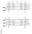
dummy wires Fig. 1 . For example, as shown inFig. 5 , thedummy wire 7b is allowed to extend from the signal wire 2b, not from thesignal wire 2a as shown inFig. 4 . - Additionally, in the arrangements as shown in
Figs. 1 and5 , thedummy wires pixel electrodes 6d through 6f which are disposed on the upper end, the lower end, and the right end; however, as shown inFigs. 6 and7 , a dummy wire 7c(third dummy wire) is further allowed to be formed at all intervals between pixel electrodes which are arranged vertically. - As described above, the dummy wires are installed so as to provide even parasitic capacities which are added to the pixel electrodes of the pixels, with respect to all pixels in the liquid crystal panel. This makes it possible to provide an even lighting display for each pixel; therefore, the display quality can be improved.
- Moreover, as described above, in the liquid crystal panel which uses the two-terminal element, in the case when the signal wire connected with the pixel is set as a data wire, a transparent electrode, which is arranged on the other transparent substrate, serves as a transparent scanning electrode. The transparent substrate opposes the substrate on which the pixel is formed. In this case, as shown in
Fig. 8 , electric charge is applied to thedummy wire 7a due to an electric effect of atransparent scanning electrode 8; therefore, it is not necessary to electrically connect thedummy wire 7a with thesignal wire 2. - Further, in the liquid crystal display device of the present embodiment, the
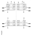
dummy wire 7a is electrically connected with the neighboringsignal wire 2. Therefore, for example, as shown inFig. 9 , even in the case of a liquid crystal panel with a centrally divided structure in which eachsignal wire 2 is divided at the center and a signal is inputted to each signal wire from above and below, an interval between pixels aligned with a division line located in between is not widened; consequently, this arrangement causes no demerit. - That is, as shown in
Fig. 10 , in the case when thedummy wire 7a is further connected with asignal wire 2 which is on the left of thesignal wire 2 adjacent to thedummy wire 7a (for example, in the case of a line reverse drive, this connection may be arranged), there is a problem: a dot pitch becomes greater at the divided part of the center, and it becomes difficult to realize this arrangement from the viewpoint of dimension. Further, the yield becomes smaller due to leak and others; consequently, the cost is increased. However, the arrangement inFig. 9 does not cause this kind of problem. - Referring to
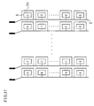
Fig. 11 , the following explanation will discuss another embodiment of the present invention. Further, with regard to the liquid crystal display device of the present embodiment, the construction of each pixel in the liquid crystal panel is the same as that ofEmbodiment 1 and the description thereof is omitted. - In the aforementioned liquid crystal panel, a
dummy wire 7d is formed so as to apply even parasitic capacities topixel electrodes 6 of the respective pixels. Thedummy wire 7d, as shown inFig. 11 , is arranged so as to surround each pixel in the liquid crystal panel together with thesignal wire 2. - In the arrangement of
Fig. 11 , thesignal wire 2 which thepixel electrode 6 is connected with (specifically, 2a inFig. 4 ) and thedummy wire 7d apply even parasitic capacities. This arrangement makes it possible to achieve an even lighting display for each pixel, thereby improving the display quality. - Furthermore, since wiring is doubled by the
dummy wire 7b and thesignal wire 2, it is possible to achieve redundancy, and to reduce wire resistance so that it becomes possible to decrease power consumption of the liquid crystal panel. - Referring to
Figs. 12 through 15 , the following explanation will discuss another liquid crystal display device, wherein the construction of each pixel in the liquid crystal panel is the same as that ofEmbodiment 1 and the description thereof is omitted. - Unlike
Embodiments Fig. 12 , the aforementioned liquid crystal panel includes no dummy wire for applying even parasitic capacities topixel electrodes 6 of the respective pixels. - In the arrangement of
Fig. 12 , with regard to the parasitic capacities C1 and C2, a sufficient interval is set between thepixel electrode 6 of each pixel and thesignal wire 2 which is adjacent to the pixel electrode 6 (hereinafter, referred to as a line interval: indicated by an arrow A inFig. 12 ); therefore, the parasitic capacities C1 and C2 are reduced so as not to affect the image display. Further, with regard to the parasitic capacities C3 and C4, an interval is set sufficiently between thepixel electrodes 6 which are arranged vertically(hereinafter, referred to as a pixel interval: indicated by an arrow B inFig. 12 ); therefore, the parasitic capacities C3 and C4 are reduced so as not to affect the image display. - Here, the following explanation will discuss a numerical limit for properly setting the line interval and pixel interval.
- In the image display of the liquid crystal panel, when a contrast difference between pixels exceeds nearly 3%, the contrast difference is recognized by visual observation. Therefore, the following description assumes that the liquid crystal panel can provide a uniform lighting display when the contrast difference is less than 3%, and the objective is to set the contrast difference at less than 3%.
-
Fig. 13 shows the relationship between a parasitic capacity ratio (a ratio of each parasitic capacity to an element capacity) and the contrast difference. As shown inFig. 13 , the parasitic capacity ratio is 5.13 % in the case when the contrast difference is 3%. Thus, it is understood that the lighting display of each pixel can be uniform by setting the parasitic capacity ratio at not more than 5%. - Here, the following explanation describes how to obtain the interval between the
pixel electrode 6 and thesignal wire 2 and the interval betweenpixel electrodes 6 for satisfying the conditions of the numerical limit of the parasitic capacity ratio. Firstly, an example of calculation of the element capacity is explained as follows. Additionally, the following calculation is based on the assumption that the dot pitch: 0.24 mm, the pixel construction: 480 × 320 dots, and the panel size: approximately 5 inches. - Considering the accuracy of a stepping projection aligner which is used for making a matrix substrate, and the capacity ratio, the area of an element is generally set at 3 µm × 3 µm to 6 µm × 6 µm. Here, the area is set at 4 µm × 5 µm as a representative value. The dielectric constant of the anodic oxidation film 4 which is made of Ta on the
lower electrode 3 is generally set at 18 to 24. Here, the dielectric constant is set at 20 as a representative value. Further, a vacuum dielectric constant ε0 is set at 8.86 × 10⁻¹²Fm-1. Moreover, the film thickness of the anodic oxidation film 4 which is made of Ta is generally set at 300 to 1000 Å. Here, the film thickness is set at 600 Å as a representative value.
- By the use of the obtained element capacity, in the liquid crystal panel in which the line interval and pixel interval vary, the parasitic capacity ratio to the element capacity is calculated by the use of the parasitic capacity which is calculated in a way shown in
Embodiment 1. And then, a graph ofFig. 13 is plotted so as to determine a numerical limit. Further, inFig. 13 , the plot of the 11.98 % parasitic capacity ratio corresponds to the case when the line interval and the pixel interval are 3 µm, and the plot of the 3.59 % parasitic capacity ratio corresponds to the case when the line interval and the pixel interval are 10 µm. Moreover, the other plots between these two plots are set at intervals of 1 µm of the line interval and the pixel interval. Namely, according toFig. 13 , when the line interval and the pixel interval are not less than 7 µm, the contrast difference can be set at not more than 3 %. - As described above, sufficient line intervals and pixel intervals are obtained (parasitic capacity is reduced) so that it becomes possible to solve the uneven lighting display caused by uneven parasitic capacities. Further, at the same time, it is possible to reduce drive voltage for lighting; consequently, low power consumption can be realized.
- Moreover, with the arrangement of
Fig. 12 , sufficient line intervals and pixel intervals are obtained so as to reduce the influence of the parasite capacities C1 through C4; therefore, it is possible to eliminate the need for arranging a dummy wire. However, as shown inFigs. 14 and15 , the following arrangement is also allowed: thedummy wire 7a is formed so as to provide the even parasitic capacities C1 and C2 with regard to all pixels, and the pixel intervals (indicated by an arrow B inFigs. 14 and15 ) are widened with regard to the parasitic capacities C3 and C4 so that it becomes possible to reduce the influence of the parasitic capacities C3 and C4. Of course, contrary to this arrangement, the following arrangement is further allowed: thedummy wire 7b is formed so as to provide the even parasitic capacities C3 and C4 with regard to all pixels, and, with regard to the parasitic capacities C1 and C2, the line intervals are widened so that it becomes possible to reduce the influence of the parasitic capacities C1 and 2. - The
aforementioned Embodiments - Firstly,
Fig. 16 shows a conventional liquid crystal display device with the simple-matrix system. As shown inFig. 16 , in the liquid crystal display device with the simple-matrix system,segment electrodes 9 andcommon electrodes 10 are formed on each of a pair of transparent substrates which oppose each other (not shown). Thesegment electrodes 9 and thecommon electrodes 10 are arranged so as to intersect one another. - With the aforementioned arrangement, a parasitic capacity appears in any of the
segment electrodes 9 and thecommon electrodes 10 due to the influence of neighboring electrodes. In this case, with regard to any electrode except for electrodes disposed on ends, the parasitic capacities are applied from electrodes disposed on both sides. However, with regard to each of the electrodes disposed on ends, a neighboring electrode exists only on one side; therefore, the parasitic capacity which is applied to each of the electrodes disposed on ends becomes smaller than the parasitic capacities applied to the electrode which is not disposed on ends, resulting in an uneven lighting display. - Hence, in the liquid display device of the present example, in order to solve the uneven lighting display, as shown in
Fig. 17 ,dummy wires 11 and 12 (electrodes indicated by slanting lines inFig. 17 ) are provided on the outside of thesegment electrodes 9 and thecommon electrodes 10 that are disposed on ends. - With this arrangement, with regard to both of the
segment electrode 9 and thecommon electrode 10, it is possible to obtain a uniform parasitic capacity of the electrode disposed on ends as well as of the electrode which is not disposed on ends; therefore, an even lighting display can be realized. - Further, besides the arrangement shown in
Fig. 17 , in the arrangement shown inFig. 18 , with regard to thesegment electrode 9 and thecommon electrode 10, intervals between neighboring electrodes (indicated by an arrow inFig. 18 ) are widened sufficiently so as to reduce the parasitic capacity between electrodes to a degree at which the display is not affected; therefore, an even lighting display can be realized. - As described above,
- (1) by providing a dummy wire for obtaining an even parasitic capacity which is applied to each pixel electrode,
- (2) or expanding an interval between a neighboring pixel and a signal wire or an interval between neighboring pixels, the influence of capacity applied to each pixel electrode is reduced so as to realize an even lighting display of the liquid crystal display device.
- With the aforementioned embodiments and examples, it becomes possible to solve the uneven lighting display merely by changing a masking pattern without increasing the number of processes and the cost.
- Namely, the liquid crystal display device of
Embodiment 1, in which a plurality of pixels forming a display screen are arranged in a matrix form and all pixels forming each pixel line are connected with asignal wire 2 for each of the pixel lines, is provided with thedummy wire 7a which is formed on the outside of the final pixel line with no neighboring signal wire other than asignal wire 2a being connected with the final pixel line, and which applies topixel electrodes dummy wire 7a is electrically connected with the neighboring signal wire (in other words, asignal wire 2a with regard to thepixel electrodes - With the aforementioned arrangement, the
dummy wire 7a applies to thepixel electrodes pixel electrodes - With this arrangement, it becomes possible to solve the uneven image display which has been caused by the difference in parasitic capacity applied to each of the pixel electrodes; consequently, an even lighting display can be realized. Further, since the
dummy wire 7a is electrically connected with the neighboring signal wire, it is easy to arrange wires. For example, even in the case of a liquid crystal display device with a centrally divided structure, this arrangement does not cause the expansion of dot pitch in a central divided portion, the decrease of yield, and other demerits. - Moreover, the liquid crystal display device is further provided with the
dummy wire 7b which is formed on the outside of the pixels disposed on both ends of the pixel lines being connected with the respective signal wires, and which applies to thepixel electrodes pixel electrodes 6b or 6c with regard topixel electrodes - With the aforementioned arrangement, the
dummy wire 7b applies the same amount of parasitic capacity as the between-pixel parasitic capacity which is applied from the neighboring pixel electrode to thepixel electrodes pixel electrodes - With this arrangement, it is possible to solve the uneven image display which has been caused by the difference in parasitic capacity applied to each of the pixel electrodes; consequently, an even lighting display can be realized.
- Further, the liquid crystal display device is allowed to be arranged so that each
signal wire 2 is divided at the center and a signal is inputted to eachsignal wire 2 from above and below. - With the aforementioned arrangement, even the liquid crystal display device having the centrally divided structure in which each
signal wire 2 is divided at the center and a signal is inputted to eachsignal wire 2 from above and below, does not cause any inconvenience such as the expansion of dot pitch in a central divided portion, making it possible to solve the uneven image display which has been caused by the difference in parasitic capacity applied to each of the pixel electrodes; consequently, an even lighting display can be realized. - Further, the liquid crystal display device is allowed to be arranged as follows: a liquid crystal display device in which a plurality of pixels forming a display screen are arranged in a matrix form and all pixels forming each pixel line are connected with a
signal wire 2 for each of the pixel lines, is provided with (a) thedummy wire 7a which is formed on the outside of the final pixel line with no neighboring signal wire other than asignal wire 2a being connected with the final pixel line and which applies topixel electrodes transparent scanning electrode 8 which is formed on a transparent substrate opposing the substrate on which thedummy wire 7a is formed, wherein thedummy wire 7a is not electrically connected with other signal wires. - With the aforementioned arrangement, the
dummy wire 7a is not electrically connected with other signal wires; however, since thetransparent scanning electrode 8 generates electric charge due to an electric effect, it is possible to apply to a pixel the same amount of parasitic capacity as the signal wire applies. Therefore, thedummy wire 7a does not make a complex wiring pattern on the substrate, thereby preventing the yield from decreasing due to leak and others. - Furthermore, with regard to the liquid crystal display device of
Embodiment 2 in which a plurality of pixels forming the display screen are arranged in a matrix form and all pixels forming each pixel line are connected with asignal wire 2 for each of the pixel lines, each of the pixel electrodes which constitute the display screen is surrounded by thedummy wires 7d having an identical shape. - With the aforementioned arrangement, all pixel electrodes are surrounded by the
dummy wires 7d having an identical shape; therefore, with regard to pixel electrodes of all pixels, it is possible to apply even parasitic capacities. - With this arrangement, it is possible to solve the uneven image display which has been caused by the difference in parasitic capacity applied to each of the pixel electrodes; consequently, an even lighting display can be realized. Further, since the
signal wire 2 is doubled by thedummy wire 7a, it is possible to achieve redundancy, and to reduce the resistance of the signal wire so that it becomes possible to decrease power consumption of the liquid crystal display device. - Moreover, with regard to the liquid crystal display device of
Embodiments - Namely, with regard to the liquid crystal display device using an MIM element as a switching element which causes the most serious defect in display in the event of uneven parasitic capacity applied to each of the pixel electrodes, it is possible to solve the uneven image display; consequently, an even lighting display can be realized.
- Furthermore, the liquid crystal display device of Example 1, in which a plurality of pixels forming a display screen are arranged in a matrix form and all pixels forming each pixel line are connected with a
signal wire 2 for each of the pixel lines, is characterized in that intervals between pixel electrodes on each pixel line as well as intervals between pixel electrodes disposed on each pixel line and thesignal wires 2 which are adjacent to the pixel electrodes are expanded so that the parasitic capacities applied to the respective pixel electrodes do not affect the display image. - With the above-mentioned arrangement, intervals between pixel electrodes on the respective pixel lines as well as intervals between pixel electrodes disposed on each pixel line and the
signal wires 2 which are adjacent to the pixel electrodes are expanded so that the influence of parasitic capacity is reduced for each pixel electrode; therefore, it is possible to solve the uneven image display which has been caused by the difference in parasitic capacity; consequently, an even lighting display can be realized. Further, at the same time, it is possible to reduce the driving voltage for lighting so as to achieve low power consumption. - The liquid crystal display device is allowed to be arranged as follows: a liquid crystal display device, in which a plurality of pixels forming a display screen are arranged in a matrix form and all pixels forming each pixel line are connected with a signal wire 2 for each of the pixel lines, is provided with (a) the dummy wire 7a which is formed on the outside of the final pixel line with no signal wire other than a signal wire 2a being connected with the final pixel line, and which applies to pixel electrodes 6d and 6f disposed on the final pixel line the same amount of parasitic capacity as a between-line parasitic capacity which is applied from the neighboring signal wire, and (b)the dummy wire 7b which is formed on the outside of the pixels disposed on both ends of the pixel lines being connected with the respective signal wires, and which applies to the pixel electrodes 6e and 6f of the pixels disposed on both ends the same amount of parasitic capacity as the between-pixel parasitic capacity which is applied from the neighboring pixel electrodes; therefore, the between-line parasitic capacity and the between-pixel parasitic capacity can be arranged so as to be uniform for each pixel electrode; and with regard to parasitic capacities which are not added by the dummy wires, those parasitic capacities applied to the respective pixel electrodes are reduced to such an extent that they do not affect the display image by sufficiently expanding intervals between pixel electrodes on each pixel line, or intervals between pixel electrodes disposed on each pixel line and the signal wires 2 which are adjacent to pixel electrodes.
- With the above-mentioned arrangement, the
dummy wires signal wires 2 which are adjacent to pixel electrodes. - With this arrangement, it is possible to solve the uneven image display that has been caused by the difference in parasitic capacity applied to each of the pixel electrodes; consequently, an even lighting display can be realized.
- Further, in the aforementioned liquid crystal display device, the pixel uses an MIM element, which is connected with the pixel electrode in series, as a switching element. It is desirable that each parasitic capacity is not more than 5% with regard to the element capacity; the parasitic capacity appearing between pixel electrodes on each pixel line, and the parasitic capacity appearing between the pixel electrodes disposed on each pixel line and the signal wires that are adjacent to the pixel electrodes.
- With the aforementioned arrangement, each parasitic capacity is set not more than 5% with regard to the element capacity: the parasitic capacity appearing between pixel electrodes disposed on the respective pixel lines, and the parasitic capacity appearing between the pixel electrodes on respective pixel lines and the signal wires that are adjacent to pixel electrodes, so that the parasitic capacities can be positively reduced so as not to affect the image display.
- Moreover, with regard to the liquid crystal display device of Example 2, in the liquid crystal display device with the simple-matrix system, in which a plurality of the
common electrodes 10 and a plurality of thesegment electrodes 9 are disposed so as to intersect one another, at least thecommon electrode 10 or thesegment electrode 9 is provided with thedummy wire - With the aforementioned arrangement, with regard to all electrodes, it is possible to achieve even parasitic capacities which appear between electrodes.
- With this arrangement, it is possible to solve the uneven image display that has been caused by the difference in parasitic capacity applied to each of the pixel electrodes; consequently, an even lighting display can be realized.
- Furthermore, the following arrangement is also preferable: in the liquid crystal display device with the simple-matrix system, in which a plurality of the
common electrodes 10 and a plurality of thesegment electrodes 9 are disposed so as to intersect one another, with regard to at least thecommon electrode 10 or thesegment electrode 9, the intervals between electrodes are sufficiently expanded so that the parasitic capacities applied to the respective electrodes do not affect the image display. - With the aforementioned arrangement, it is possible to reduce the parasitic capacities applied to the respective electrodes so as not to affect the image display.
- The invention being thus described, it will be obvious that the same may be varied in many ways. Such variations are not to be regarded as a departure from the scope of the invention as defined by the following claims.
Claims (12)
- A liquid crystal display device comprising a plurality of pixels, which form a display screen and are arranged in a matrix form, and signal wires (2), wherein all pixels forming a respective pixel line of said matrix are connected with a corresponding signal wire (2), said display device further comprising:a first dummy wire(7a) which is formed along an outside of a final pixel line with no neighboring signal wire other than a final signal wire (2a) being connected with the final pixel line, and which is arranged to apply to the pixel electrodes (6d-6f) disposed on the final pixel line the same amount of parasitic capacity as a between-line parasitic capacity which is applied from a neighboring signal wire, wherein said first dummy wire is electrically connected with the neighboring final signal wire,characterized in thatthe liquid crystal display device , further comprises second dummy wires (7b) which are formed on the respective outside of the pixels disposed on both ends of the pixel lines, each second dummy wire being connected with a respective signal wire, and being arranged to apply to the pixel electrodes (6e-6f) of the pixels disposed on both ends the same amount of parasitic capacity as a between-pixel parasitic capacity which is applied from the neighboring pixel electrode in the pixel line.
- A liquid crystal display device comprising a plurality of pixels, which form a display screen and are arranged in a matrix form, and signal wires (2), wherein all pixels forming a respective pixel line of said matrix are connected with a corresponding signal wire (2), said display device further comprising:a first dummy wire (7a) which is formed along an outside of a final pixel line with no neighboring signal wire other than a final signal wire (2a) being connected with the final pixel line and which is arranged to apply to the pixel electrodes (6d-6f) disposed on the final pixel line the same amount of parasitic capacity as a between-line parasitic capacity which is applied from the neighboring signal wire,characterized in thatthe liquid crystal display device further comprises a transparent scanning electrode(8) which is formed on a transparent substrate opposing a substrate on which said first dummy wire (7a) is formed, said first dummy wire being electrically connected with none of the signal wires, but being electrically charged due to an electric effect of the transparent scanning electrode, and second dummy wires (7b) which are formed on the respective outside of the pixels disposed on both ends of the pixel lines each second dummy wire being connected with a respective signal wire, and being arranged to apply to the pixel electrodes (6e-6f) of the pixels disposed on both ends the same amount of parasitic capacity as a between-pixel parasitic capacity which is applied from the neighboring pixel electrode in the pixel line.
- The liquid crystal display device as defined in claim 1 or 2, wherein a respective second dummy wire(7b) extends from the signal wire(2a) which is connected with the pixel electrode, to which said second dummy wire applies the parasitic capacity.
- The liquid crystal display device as defined in claim 1 or 2, wherein a respective second dummy wire(7b) extends from a signal wire(2b) which is not connected with the pixel electrode, to which said second dummy wire applies the parasitic capacity.
- The liquid crystal display device as defined in any one of claims 1 through 4, further comprising third dummy wires (7c) which are provided between neighboring pixel electrodes in the pixel lines, the third dummy wires being connected with a respective signal wire (2) so as to apply an even parasitic capacity to the neighboring pixel electrode.
- The liquid crystal display device as defined in claim 5, wherein a respective third dummy wire(7c) extends from the signal wire (2a) which is connected with the pixel electrode, to which said third dummy wire applies the parasitic capacity.
- The liquid crystal display device as defined in claim 5, wherein a respective third dummy wire(7c) extends from a signal wire(2b) which is not connected with the pixel electrode, to which said third dummy wire applies the parasitic capacity.
- The liquid crystal display device as defined in any one of claims 1 through 7, wherein said signal wires (2) are divided at a center and arranged such that a signal can be inputted to each signal wire from both ends of the signal wires.
- The liquid crystal display device, as defined in any one of claims 5 through 7, wherein the first, second and third dummy wires are arranged such that each of the pixel electrodes constituting said display panel is surrounded by a dummy wire (7d) having an identical shape.
- The liquid crystal display device as defined in any one of claims 1 through 9, wherein each of said pixels comprises a mettal-insulator-metal MIM element which is connected with the pixel electrode in series, as a switching element.
- The liquid crystal display device, as defined in any of claims 1 through 10,
characterized in that an interval between pixel electrodes on each pixel line as well as an interval between the pixel electrode disposed on each pixel line and the signal wire which is adjacent to the pixel electrode are expanded so that, with regard to parasitic capacities which are not added by the dummy wires, but consist of the between-line parasitic capacity and the etweenpixel parasitic capacity each parasitic capacity applied to each pixel electrode is not more than 5% with regard to the element capacity. - The liquid crystal display device as defined in any of claims 1 to 11, wherein the between-line parasitic capacity and the between-pixel parasitic capacity is arranged so as to be uniform for each pixel electrode.
Applications Claiming Priority (2)
| Application Number | Priority Date | Filing Date | Title |
|---|---|---|---|
| JP36124597 | 1997-12-26 | ||
| JP36124597A JP3335895B2 (en) | 1997-12-26 | 1997-12-26 | Liquid crystal display |
Publications (3)
| Publication Number | Publication Date |
|---|---|
| EP0926537A2 EP0926537A2 (en) | 1999-06-30 |
| EP0926537A3 EP0926537A3 (en) | 1999-07-14 |
| EP0926537B1 true EP0926537B1 (en) | 2012-05-09 |
Family
ID=18472793
Family Applications (1)
| Application Number | Title | Priority Date | Filing Date |
|---|---|---|---|
| EP98123364A Expired - Lifetime EP0926537B1 (en) | 1997-12-26 | 1998-12-08 | Liquid crystal display device |
Country Status (3)
| Country | Link |
|---|---|
| US (2) | US6333771B1 (en) |
| EP (1) | EP0926537B1 (en) |
| JP (1) | JP3335895B2 (en) |
Families Citing this family (16)
| Publication number | Priority date | Publication date | Assignee | Title |
|---|---|---|---|---|
| KR20020052137A (en) * | 2000-12-23 | 2002-07-02 | 구본준, 론 위라하디락사 | Liquid crystal display |
| KR100394026B1 (en) * | 2000-12-27 | 2003-08-06 | 엘지.필립스 엘시디 주식회사 | Liquid crystal device and method for driving the same |
| JP2002244585A (en) * | 2001-02-02 | 2002-08-30 | Koninkl Philips Electronics Nv | Picture display device |
| US20030016318A1 (en) * | 2001-07-23 | 2003-01-23 | Wei-Chen Liang | Color display |
| JP3730161B2 (en) | 2001-11-28 | 2005-12-21 | シャープ株式会社 | Liquid crystal display device |
| JP3666662B2 (en) * | 2002-12-13 | 2005-06-29 | シャープ株式会社 | Display device |
| CN1300753C (en) * | 2003-02-10 | 2007-02-14 | 三洋电机株式会社 | Dynamic matrix type display device |
| TWI274316B (en) * | 2003-12-15 | 2007-02-21 | Tpo Displays Corp | Display circuitry of display panel |
| JP4184334B2 (en) * | 2003-12-17 | 2008-11-19 | シャープ株式会社 | Display device driving method, display device, and program |
| KR100635061B1 (en) * | 2004-03-09 | 2006-10-17 | 삼성에스디아이 주식회사 | Flat Panel Display and method of fabricating the same |
| JP2005257929A (en) * | 2004-03-10 | 2005-09-22 | Sanyo Electric Co Ltd | Active matrix display device |
| JP2007184125A (en) * | 2006-01-05 | 2007-07-19 | Seiko Epson Corp | Light-emitting device and image printer |
| US9285909B2 (en) * | 2010-04-09 | 2016-03-15 | Apple Inc. | Equalizing parasitic capacitance effects in touch screens |
| JP5639819B2 (en) * | 2010-08-30 | 2014-12-10 | 株式会社ジャパンディスプレイ | Display device |
| US9329738B2 (en) * | 2012-09-10 | 2016-05-03 | Apple Inc. | Determination and reduction of parasitic capacitance variation due to display noise |
| KR102058855B1 (en) * | 2013-12-31 | 2019-12-26 | 엘지디스플레이 주식회사 | Display device |
Citations (2)
| Publication number | Priority date | Publication date | Assignee | Title |
|---|---|---|---|---|
| JPH0572557A (en) * | 1991-09-17 | 1993-03-26 | Hitachi Ltd | Liquid crystal matrix display device |
| JPH0713177A (en) * | 1993-06-28 | 1995-01-17 | Toshiba Corp | Liquid crystal display device |
Family Cites Families (25)
| Publication number | Priority date | Publication date | Assignee | Title |
|---|---|---|---|---|
| US5177743A (en) | 1982-02-15 | 1993-01-05 | Hitachi, Ltd. | Semiconductor memory |
| JPS61140982A (en) | 1984-12-12 | 1986-06-28 | シャープ株式会社 | Liquid crystal display |
| JPS624724U (en) | 1985-06-03 | 1987-01-12 | ||
| DE3523206A1 (en) | 1985-06-28 | 1987-01-02 | Bayer Ag | METHOD FOR PRODUCING POLY (DIORGANOSILOXANES) WITH ALKOXY END GROUPS |
| JPS6258226A (en) | 1985-09-09 | 1987-03-13 | Seiko Epson Corp | Liquid crystal display body |
| JPS643630A (en) | 1987-06-26 | 1989-01-09 | Seiko Instr & Electronics | Electro-optic device |
| JP2590992B2 (en) | 1987-07-02 | 1997-03-19 | セイコーエプソン株式会社 | Liquid crystal device and driving method thereof |
| JPH01133032A (en) | 1987-11-18 | 1989-05-25 | Seiko Instr & Electron Ltd | Electrooptic device |
| JPH027024A (en) | 1988-06-27 | 1990-01-11 | Fujitsu Ltd | Thin film transistor matrix |
| JP2508301B2 (en) | 1989-10-23 | 1996-06-19 | 日本電気株式会社 | Semiconductor integrated circuit |
| JPH0473951A (en) | 1990-07-16 | 1992-03-09 | Nec Ic Microcomput Syst Ltd | Semiconductor device |
| KR960014823B1 (en) * | 1991-03-15 | 1996-10-21 | 가부시기가이샤 히다찌세이사구쇼 | Liquid crystal display device |
| JPH0527268A (en) | 1991-07-23 | 1993-02-05 | Toshiba Corp | Liquid crystal display device |
| JPH05249478A (en) * | 1991-12-25 | 1993-09-28 | Toshiba Corp | Liquid crystal display device |
| JPH0728096A (en) | 1993-07-14 | 1995-01-31 | Toshiba Corp | Liquid crystal display device and its production |
| JP3322948B2 (en) | 1993-09-17 | 2002-09-09 | 株式会社東芝 | Array substrate for display device and liquid crystal display device |
| TW373094B (en) * | 1994-11-14 | 1999-11-01 | Hitachi Device Engineering Corp | Liquid crystal display device having a uniform liquid crystal layer thickness |
| US6169530B1 (en) * | 1995-04-20 | 2001-01-02 | Canon Kabushiki Kaisha | Display apparatus and assembly of its driving circuit |
| US5767929A (en) * | 1995-09-21 | 1998-06-16 | Advanced Display Inc. | Liquid crystal display apparatus with shorting ring |
| JP3412390B2 (en) * | 1996-03-18 | 2003-06-03 | 株式会社ニコン | Photoelectric conversion device |
| JP3256730B2 (en) * | 1996-04-22 | 2002-02-12 | シャープ株式会社 | Liquid crystal display device and driving method thereof |
| US6014191A (en) * | 1996-07-16 | 2000-01-11 | Samsung Electronics Co., Ltd. | Liquid crystal display having repair lines that cross data lines twice and cross gate lines in the active area and related repairing methods |
| US5982470A (en) * | 1996-08-29 | 1999-11-09 | Sharp Kabushiki Kaisha | Liquid crystal display device having dummy electrodes with interleave ratio same on all sides |
| KR100228282B1 (en) * | 1996-09-17 | 1999-11-01 | 윤종용 | Liquid display device |
| KR100260611B1 (en) * | 1997-04-03 | 2000-07-01 | 윤종용 | Lcd panel for reparing lines |
-
1997
- 1997-12-26 JP JP36124597A patent/JP3335895B2/en not_active Expired - Fee Related
-
1998
- 1998-12-08 EP EP98123364A patent/EP0926537B1/en not_active Expired - Lifetime
- 1998-12-08 US US09/207,403 patent/US6333771B1/en not_active Expired - Lifetime
-
2001
- 2001-11-30 US US09/996,936 patent/US6608655B2/en not_active Expired - Fee Related
Patent Citations (2)
| Publication number | Priority date | Publication date | Assignee | Title |
|---|---|---|---|---|
| JPH0572557A (en) * | 1991-09-17 | 1993-03-26 | Hitachi Ltd | Liquid crystal matrix display device |
| JPH0713177A (en) * | 1993-06-28 | 1995-01-17 | Toshiba Corp | Liquid crystal display device |
Also Published As
| Publication number | Publication date |
|---|---|
| JPH11194370A (en) | 1999-07-21 |
| US6333771B1 (en) | 2001-12-25 |
| US20020033924A1 (en) | 2002-03-21 |
| EP0926537A2 (en) | 1999-06-30 |
| US6608655B2 (en) | 2003-08-19 |
| JP3335895B2 (en) | 2002-10-21 |
| EP0926537A3 (en) | 1999-07-14 |
Similar Documents
| Publication | Publication Date | Title |
|---|---|---|
| EP0926537B1 (en) | Liquid crystal display device | |
| KR100361626B1 (en) | Active matrix liquid crystal display apparatus | |
| EP0399846B1 (en) | An active-matrix display device and a method for the production of the same | |
| US6226057B1 (en) | Liquid crystal display having overlapped pixel electrodes and method for fabricating the same | |
| US5870163A (en) | LCD device with connection lines having different resistances | |
| JPH10142633A (en) | Thin film transistor integrated device, manufacture thereof, and liquid crystal display device | |
| KR19980028450A (en) | Flat Drive Liquid Crystal Display | |
| US5847684A (en) | Display device with mirror-symmetrical pixels | |
| EP0605176B1 (en) | An active matrix type liquid crystal display panel and a method for producing the same | |
| US20030122976A1 (en) | Liquid crystal display having shorting bar for testing thin film transistor | |
| US7876388B2 (en) | Array substrate capable of improving display quality | |
| JP3636192B2 (en) | Liquid crystal device and electronic device | |
| JP3209652B2 (en) | Liquid crystal display | |
| US6888603B2 (en) | IPS-LCD with a compensation structure for reducing transmittance difference | |
| JPH0827465B2 (en) | Plane display | |
| JP3092747B2 (en) | Active matrix display device | |
| US5568289A (en) | Liquid crystal display device | |
| KR100361624B1 (en) | Liquid crystal display apparatus | |
| JP2775892B2 (en) | Two-terminal element type liquid crystal display | |
| JP3380857B2 (en) | Liquid crystal display | |
| JP2551343B2 (en) | Liquid crystal display | |
| JP3480682B2 (en) | Liquid crystal display | |
| JP2526949Y2 (en) | Matrix type liquid crystal display | |
| JP2692685B2 (en) | LCD panel | |
| JP3380856B2 (en) | Liquid crystal display |
Legal Events
| Date | Code | Title | Description |
|---|---|---|---|
| PUAI | Public reference made under article 153(3) epc to a published international application that has entered the european phase |
Free format text: ORIGINAL CODE: 0009012 |
|
| PUAL | Search report despatched |
Free format text: ORIGINAL CODE: 0009013 |
|
| AK | Designated contracting states |
Kind code of ref document: A2 Designated state(s): DE GB |
|
| AX | Request for extension of the european patent |
Free format text: AL;LT;LV;MK;RO;SI |
|
| AK | Designated contracting states |
Kind code of ref document: A3 Designated state(s): AT BE CH CY DE DK ES FI FR GB GR IE IT LI LU MC NL PT SE |
|
| AX | Request for extension of the european patent |
Free format text: AL;LT;LV;MK;RO;SI |
|
| 17P | Request for examination filed |
Effective date: 19991014 |
|
| AKX | Designation fees paid |
Free format text: DE GB |
|
| 17Q | First examination report despatched |
Effective date: 20060328 |
|
| REG | Reference to a national code |
Ref country code: DE Ref legal event code: R079 Ref document number: 69842713 Country of ref document: DE Free format text: PREVIOUS MAIN CLASS: G02F0001134300 Ipc: G02F0001136200 |
|
| GRAP | Despatch of communication of intention to grant a patent |
Free format text: ORIGINAL CODE: EPIDOSNIGR1 |
|
| GRAJ | Information related to disapproval of communication of intention to grant by the applicant or resumption of examination proceedings by the epo deleted |
Free format text: ORIGINAL CODE: EPIDOSDIGR1 |
|
| GRAC | Information related to communication of intention to grant a patent modified |
Free format text: ORIGINAL CODE: EPIDOSCIGR1 |
|
| GRAP | Despatch of communication of intention to grant a patent |
Free format text: ORIGINAL CODE: EPIDOSNIGR1 |
|
| RIC1 | Information provided on ipc code assigned before grant |
Ipc: G02F 1/1365 20060101ALI20111130BHEP Ipc: G02F 1/1362 20060101AFI20111130BHEP |
|
| GRAS | Grant fee paid |
Free format text: ORIGINAL CODE: EPIDOSNIGR3 |
|
| GRAA | (expected) grant |
Free format text: ORIGINAL CODE: 0009210 |
|
| AK | Designated contracting states |
Kind code of ref document: B1 Designated state(s): DE GB |
|
| REG | Reference to a national code |
Ref country code: GB Ref legal event code: FG4D |
|
| REG | Reference to a national code |
Ref country code: DE Ref legal event code: R096 Ref document number: 69842713 Country of ref document: DE Effective date: 20120628 |
|
| PGFP | Annual fee paid to national office [announced via postgrant information from national office to epo] |
Ref country code: GB Payment date: 20121205 Year of fee payment: 15 |
|
| PLBE | No opposition filed within time limit |
Free format text: ORIGINAL CODE: 0009261 |
|
| STAA | Information on the status of an ep patent application or granted ep patent |
Free format text: STATUS: NO OPPOSITION FILED WITHIN TIME LIMIT |
|
| 26N | No opposition filed |
Effective date: 20130212 |
|
| PGFP | Annual fee paid to national office [announced via postgrant information from national office to epo] |
Ref country code: DE Payment date: 20121219 Year of fee payment: 15 |
|
| REG | Reference to a national code |
Ref country code: DE Ref legal event code: R097 Ref document number: 69842713 Country of ref document: DE Effective date: 20130212 |
|
| REG | Reference to a national code |
Ref country code: DE Ref legal event code: R119 Ref document number: 69842713 Country of ref document: DE |
|
| GBPC | Gb: european patent ceased through non-payment of renewal fee |
Effective date: 20131208 |
|
| REG | Reference to a national code |
Ref country code: DE Ref legal event code: R119 Ref document number: 69842713 Country of ref document: DE Effective date: 20140701 |
|
| PG25 | Lapsed in a contracting state [announced via postgrant information from national office to epo] |
Ref country code: DE Free format text: LAPSE BECAUSE OF NON-PAYMENT OF DUE FEES Effective date: 20140701 |
|
| PG25 | Lapsed in a contracting state [announced via postgrant information from national office to epo] |
Ref country code: GB Free format text: LAPSE BECAUSE OF NON-PAYMENT OF DUE FEES Effective date: 20131208 |