EP0925709B1 - Organic light-emitting devices with improved cathode - Google Patents
Organic light-emitting devices with improved cathode Download PDFInfo
- Publication number
- EP0925709B1 EP0925709B1 EP97939034A EP97939034A EP0925709B1 EP 0925709 B1 EP0925709 B1 EP 0925709B1 EP 97939034 A EP97939034 A EP 97939034A EP 97939034 A EP97939034 A EP 97939034A EP 0925709 B1 EP0925709 B1 EP 0925709B1
- Authority
- EP
- European Patent Office
- Prior art keywords
- layer
- conductive material
- organic light
- emitting device
- cathode
- Prior art date
- Legal status (The legal status is an assumption and is not a legal conclusion. Google has not performed a legal analysis and makes no representation as to the accuracy of the status listed.)
- Expired - Lifetime
Links
Images
Classifications
-
- H—ELECTRICITY
- H05—ELECTRIC TECHNIQUES NOT OTHERWISE PROVIDED FOR
- H05B—ELECTRIC HEATING; ELECTRIC LIGHT SOURCES NOT OTHERWISE PROVIDED FOR; CIRCUIT ARRANGEMENTS FOR ELECTRIC LIGHT SOURCES, IN GENERAL
- H05B33/00—Electroluminescent light sources
- H05B33/12—Light sources with substantially two-dimensional [2D] radiating surfaces
- H05B33/26—Light sources with substantially two-dimensional [2D] radiating surfaces characterised by the composition or arrangement of the conductive material used as an electrode
-
- H—ELECTRICITY
- H05—ELECTRIC TECHNIQUES NOT OTHERWISE PROVIDED FOR
- H05B—ELECTRIC HEATING; ELECTRIC LIGHT SOURCES NOT OTHERWISE PROVIDED FOR; CIRCUIT ARRANGEMENTS FOR ELECTRIC LIGHT SOURCES, IN GENERAL
- H05B33/00—Electroluminescent light sources
- H05B33/10—Apparatus or processes specially adapted to the manufacture of electroluminescent light sources
-
- H—ELECTRICITY
- H05—ELECTRIC TECHNIQUES NOT OTHERWISE PROVIDED FOR
- H05B—ELECTRIC HEATING; ELECTRIC LIGHT SOURCES NOT OTHERWISE PROVIDED FOR; CIRCUIT ARRANGEMENTS FOR ELECTRIC LIGHT SOURCES, IN GENERAL
- H05B33/00—Electroluminescent light sources
- H05B33/12—Light sources with substantially two-dimensional [2D] radiating surfaces
-
- H—ELECTRICITY
- H10—SEMICONDUCTOR DEVICES; ELECTRIC SOLID-STATE DEVICES NOT OTHERWISE PROVIDED FOR
- H10K—ORGANIC ELECTRIC SOLID-STATE DEVICES
- H10K50/00—Organic light-emitting devices
- H10K50/80—Constructional details
- H10K50/805—Electrodes
- H10K50/82—Cathodes
- H10K50/826—Multilayers, e.g. opaque multilayers
-
- H—ELECTRICITY
- H10—SEMICONDUCTOR DEVICES; ELECTRIC SOLID-STATE DEVICES NOT OTHERWISE PROVIDED FOR
- H10K—ORGANIC ELECTRIC SOLID-STATE DEVICES
- H10K2102/00—Constructional details relating to the organic devices covered by this subclass
- H10K2102/301—Details of OLEDs
- H10K2102/351—Thickness
Definitions
- the field of the invention relates to organic light-emitting devices with efficient electron injecting electrodes.
- OLEDs Organic light-emitting devices
- an OLED consists of an anode that injects positive charge carriers, a cathode that injects negative charge carriers and at least one organic electroluminescent layer sandwiched between the two electrodes.
- One of the key advantages of the OLED technology is that devices can be operated at low drive voltages, provided that suitable electro-luminescent organic layers, and electrodes with good efficiencies for the injection of positive and negative charge carriers, are used.
- the anode is a thin film of, for example, indium-tin-oxide (ITO), which is a semi-transparent conductive oxide which is commercially readily available already deposited on glass or plastic substrates.
- ITO indium-tin-oxide
- the organic layer(s) is normally deposited onto the ITO-coated substrate by, for example, evaporation, or any one of spin-coating, blade-coating, dip-coating or meniscus-coating.
- the final step of depositing the cathode layer onto the top organic layer is normally performed by thermal evaporation or sputtering of a suitable cathode metal.
- Layers of Al, Ca or alloys of Mg:Ag or Mg:In or Al alloys are often used as cathode materials. In order to achieve good performance in OLEDs it is of great importance to optimise all individual layers, the anode, the cathode and the organic layer(s), as well as the interfaces between the layers.
- cathode materials with a low work function to achieve efficient electron injection and low operating voltages.
- Such cathodes for OLEDs are typically alkali metals such as Li, Na, K, Rb or Cs, alkaline earth metals such as Mg, Ca, Sr or Ba or lanthanides such as Sm, Eu, Tb or Yb. These materials tend to react very readily with oxygen and moisture and particular care has to be taken on handling and/or during and after deposition onto OLEDs.
- these low work function materials are deposited as cathode layers onto OLEDs in the form of alloys whereby other alloy constituents stabilise the cathode layer; typical such alloys are for example Mg:Al, Mg:In or Mg:Ag or Al:Li.
- these low work function elements for instance Ca, K, Li or Sm in pure or alloy form as OLED cathode layers these elements can diffuse into the organic layer(s) and subsequently dope the organic layer(s), cause electrical shorts or quench photo-luminescence, and therefore generally deteriorate device performance.
- EP-A-0468439 discloses an organic electroluminescent device comprised of a support, an anode, an organic electroluminescent medium and a cathode.
- the cathode is comprised of a capping layer containing at least one alkaline earth or rare earth metal and interposed between the capping layer and the organic electroluminescent medium, an electron injecting layer containing at least one metal having a work function of less than 3.5eV but exhibiting a higher work function than the alkaline earth metals in the capping layer.
- EP-A-0684753 discloses an organic thin film electroluminescent diode comprising a cathode formed of a metal or alloy containing 0.01 to 5 mol% of scandium and 0.01 to 0.3 mol% if alkali metal.
- US-A-5,059,862 discloses an internal junction electroluminescent device with a cathode comprising a layer contacting an organic hole injection and transporting zone containing a combination of magnesium and aluminium. Aluminium accounts for at least 80 per cent of the cathode.
- an organic light-emitting device comprising at least one layer of a light-emissive organic material arranged between an anode and a cathode for the device, wherein the cathode comprises a first layer of a conductive material which is an opaque metallic layer and a second layer of a conductive material having a low work function arranged between the at least one layer of organic material and the first layer of conductive material, wherein the second layer of conductive material is thinner than the first layer of conductive material and comprises an elemental metal, an alloy or an intermetallic compound having a work function of at most 3.7 eV, characterised in that the second layer has a thickness of at most 5 nm.
- the cathode is composed of a thin layer of an elemental metal, alloy or inter-metallic compound, with a work function of at most 3.7 eV, but preferably less than 3.2 eV.
- the cathode layer has a thickness of at most 5 nm, but preferably of between 0.5 and 2 nm thick.
- the thin, low work function cathode layer is capped with another conductive layer, typically 100 - 500 nm thick, which provides high conductivity protection for the underlying thin, low work function layer, as well as environmental stability.
- Such a bilayer electrode structure according to the first aspect of the present invention forms a cathode layer with efficient electron injection for an OLED with at least one electro-luminescent organic layer between said cathode layer and an anode layer, the anode layer for injecting positive charge carriers.
- Such a structure prevents excessive doping and minimises the risk of shorting of the device structure and quenching of the electro-luminescence of the at least one layer of organic material.
- the first aspect of the invention also provides a method of fabricating an organic light-emitting device, comprising the steps of forming a cathode for the device over a substrate, which step comprises forming a first layer of a conductive material over a substrate and forming a second layer of a conductive material having a low work function over the first layer of conductive material, wherein the first layer of conductive material is an opaque metallic layer and the second layer of conductive material is thinner than the first layer of conductive material having a thickness of at most 5 nm, and comprises an elemental metal, an alloy or an intermetallic compound having a work function of at most 3.7 eV, forming at least one layer of a light-emissive organic material over the cathode and forming an anode for the device over the at least one layer of organic material.
- the first aspect of the invention further provides a method of fabricating an organic light-emitting device, comprising the steps of forming an anode for the device over a substrate, forming at least one layer of a light-emissive material over the anode and forming a cathode for the device over the at least one layer of organic material, which step comprises forming a second layer of a conductive material having a low work function over the at least one layer of organic material and forming a first layer of a conductive material over the second layer of conductive material, wherein the first layer of conductive material is an opaque metallic layer and the second layer of conductive material is thinner than the first layer of conductive material and comprises an elemental metal, an alloy or an intermetallic compound having a work function of at most 3.7 eV, characterised in that the second layer has a thickness of at most 5 nm.
- an OLED with an efficient electron-injecting electrode in which at least one electro-luminescent organic layer, preferably either polymeric or molecular, is deposited preferably onto a supportive substrate precoated with an anode.
- the organic layer is coated in one embodiment by vacuum evaporation, with a thin layer of conductive, low work function material.
- This layer is at most 5 nm but preferably between 0.5 and 2 nm thick, and still more preferably about 0.5 nm.
- This thin layer is typically, but not essentially, an alkali metal, alkaline earth metal or a lanthanide or an alloy or inter-metallic compound incorporating one or more of said alkali metal, alkaline earth metal or lanthanide elements.
- the thin low work function layer is then preferably covered with a thick conductive layer of typically 100 to 500 nm thickness which provides high conductivity, protection for the underlying thin low work function layer and environmental stability, and which is preferably applied by vacuum evaporation or sputter deposition.
- one or both of the first and second conductive layers are deposited using DC magnetron sputtering.
- an OLED is formed by first forming a semi-transparent anode deposited onto a transparent supportive substrate.
- the substrate is, for example, a thin sheet of glass or plastic such as polyester, polycarbonate, polyimide, poly-ether-imide or the like.
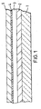
- a glass substrate 1 is covered with a layer of a semi-transparent conductive indium-tin-oxide (ITO) layer 2, typically about 150 nm thick with a sheet resistance of typically ⁇ 30 Ohms/square.
- ITO indium-tin-oxide
- the semi-transparent anode shown in Figure 1 is a thin layer of conductive oxide such as indium-tin-oxide, it may alternatively be a doped tin-oxide or zinc-oxide.
- the organic layer(s) deposited on top of the anode/substrate is/are preferably, but not necessarily, one or more layers of an electroluminescent conjugated polymer such as described in earlier US No. 5,247,190 assigned to Cambridge Display Technology Limited. Such organic layer is formed to a thickness typically of the order of 100 nm thick.
- the organic layer(s) could be low molecular weight compounds such as described in US patent No. 4,539,507, or a combination of layer(s) of conjugated polymer(s) with layer(s) of low molecular weight compound(s).
- the ITO layer is covered with a ca. 100 nm thick layer 3 of the electroluminescent polymer poly( p -phenylene vinylene), PPV, as for example described in US patent No. 5,247,190.
- the cathode may be a thin layer of an alkali metal, alkaline earth metal or a lanthanide or an alloy or inter-metallic compound incorporating one or more of said alkali metal, alkaline earth metal or lanthanide elements.
- the cathode layer is at most 5 nm but preferably between 0.5 and 2 nm thick and examples for materials which may be used are Li, K, Sm, Ca or an Al:Li alloy.
- the PPV layer 3 is preferably covered with a 0.5 nm thick layer 4 of Li deposited by vacuum sublimation of the Li from a commercial Al:Li alloy.
- the thin layer of the cathode may be sputter deposited, preferably by DC magnetron sputtering or RF sputtering.
- the thin layer of the cathode may also be evaporated, preferably by resistive evaporation or electron beam thermal evaporation.
- the thin layer of the cathode being a conductive material comprising either an elemental metal, an alloy or an intermetallic compound having a work function of at most 3.7 eV, and preferably at most 3.2 eV.
- the thin layer is then preferably covered with a conductive layer of, for example, aluminium or an aluminium alloy which is typically between 100 and 500 nm thick, and preferably about 100 nm.
- a conductive layer of, for example, aluminium or an aluminium alloy which is typically between 100 and 500 nm thick, and preferably about 100 nm.
- the thin layer 4 is, without breaking vacuum, preferably covered with a 150 nm thick layer 5 of Aluminium deposited by vacuum evaporation.
- the thick conductive layer may be sputtered, preferably by DC magnetron sputtering or RF sputtering.
- the thick layer may also be evaporated by resistive evaporation or electron-beam thermal evaporation.
- the ratio of the thickness of the thick conductive layer to the thin layer is 20:1.
- the layer thicknesses are controlled by a standard quartz crystal thickness monitor in combination with a shutter.
- the two-layer cathode described with reference to Figure 1 is formed on the substrate, the at least one layer of a light-emissive organic material is formed over the cathode, and the anode formed over the at least one layer of light-emissive organic material.
- the thin layer of Li provides excellent electron injection and low turn-on and operating voltage and, although diffusion of the Li from layer 4 into the PPV layer 3 with subsequent doping and quenching of electro-luminescence in the PPV is not prohibited, the limited thickness and hence amount of material of layer 4 prevents excessive doping and electro-luminescence quenching.
Landscapes
- Engineering & Computer Science (AREA)
- Manufacturing & Machinery (AREA)
- Physics & Mathematics (AREA)
- Optics & Photonics (AREA)
- Electroluminescent Light Sources (AREA)
- Luminescent Compositions (AREA)
Applications Claiming Priority (7)
| Application Number | Priority Date | Filing Date | Title |
|---|---|---|---|
| GB9618473 | 1996-09-04 | ||
| GB9618475 | 1996-09-04 | ||
| GBGB9618474.2A GB9618474D0 (en) | 1996-09-04 | 1996-09-04 | Organic light-emitting devices with improved cathode |
| GBGB9618473.4A GB9618473D0 (en) | 1996-09-04 | 1996-09-04 | Organic light-emitting devices with improved anode |
| GBGB9618475.9A GB9618475D0 (en) | 1996-09-04 | 1996-09-04 | Electrode deposition for organic light-emitting devices |
| GB9618474 | 1996-09-04 | ||
| PCT/GB1997/002380 WO1998010621A1 (en) | 1996-09-04 | 1997-09-04 | Organic light-emitting devices with improved cathode |
Publications (2)
| Publication Number | Publication Date |
|---|---|
| EP0925709A1 EP0925709A1 (en) | 1999-06-30 |
| EP0925709B1 true EP0925709B1 (en) | 2003-08-13 |
Family
ID=27268458
Family Applications (1)
| Application Number | Title | Priority Date | Filing Date |
|---|---|---|---|
| EP97939034A Expired - Lifetime EP0925709B1 (en) | 1996-09-04 | 1997-09-04 | Organic light-emitting devices with improved cathode |
Country Status (7)
| Country | Link |
|---|---|
| US (1) | US6255774B1 (https=) |
| EP (1) | EP0925709B1 (https=) |
| JP (3) | JP3786969B2 (https=) |
| CN (1) | CN1108730C (https=) |
| AT (1) | ATE247372T1 (https=) |
| DE (1) | DE69724129T2 (https=) |
| WO (1) | WO1998010621A1 (https=) |
Families Citing this family (126)
| Publication number | Priority date | Publication date | Assignee | Title |
|---|---|---|---|---|
| US5408109A (en) | 1991-02-27 | 1995-04-18 | The Regents Of The University Of California | Visible light emitting diodes fabricated from soluble semiconducting polymers |
| US6452218B1 (en) * | 1997-06-10 | 2002-09-17 | Uniax Corporation | Ultra-thin alkaline earth metals as stable electron-injecting electrodes for polymer light emitting diodes |
| GB9903251D0 (en) | 1999-02-12 | 1999-04-07 | Cambridge Display Tech Ltd | Opto-electric devices |
| US6849869B1 (en) | 1999-07-19 | 2005-02-01 | Dupont Displays, Inc. | Long lifetime polymer light-emitting devices with improved luminous efficiency and improved radiance |
| US6639357B1 (en) * | 2000-02-28 | 2003-10-28 | The Trustees Of Princeton University | High efficiency transparent organic light emitting devices |
| JP2002216976A (ja) * | 2001-01-15 | 2002-08-02 | Sony Corp | 発光素子及びその製造方法 |
| US6692662B2 (en) * | 2001-02-16 | 2004-02-17 | Elecon, Inc. | Compositions produced by solvent exchange methods and uses thereof |
| US6777249B2 (en) * | 2001-06-01 | 2004-08-17 | Semiconductor Energy Laboratory Co., Ltd. | Method of repairing a light-emitting device, and method of manufacturing a light-emitting device |
| GB2379317A (en) * | 2001-08-30 | 2003-03-05 | Cambridge Display Tech Ltd | Optoelectronic display operating by photoluminescence quenching |
| SG142163A1 (en) | 2001-12-05 | 2008-05-28 | Semiconductor Energy Lab | Organic semiconductor element |
| US7696303B2 (en) | 2002-05-10 | 2010-04-13 | Cambridge Display Technology Limited | Polymers their preparation and uses |
| EP1388903B1 (en) * | 2002-08-09 | 2016-03-16 | Semiconductor Energy Laboratory Co., Ltd. | Organic electroluminescent device |
| TWI272874B (en) | 2002-08-09 | 2007-02-01 | Semiconductor Energy Lab | Organic electroluminescent device |
| EP1537612B1 (en) | 2002-09-03 | 2010-05-19 | Cambridge Display Technology Limited | Method of forming an optical device |
| GB0223510D0 (en) * | 2002-10-10 | 2002-11-13 | Cambridge Display Tech Ltd | Optical device |
| EP1416028A1 (en) | 2002-10-30 | 2004-05-06 | Covion Organic Semiconductors GmbH | New method for the production of monomers useful in the manufacture of semiconductive polymers |
| KR100844803B1 (ko) * | 2002-11-19 | 2008-07-07 | 엘지디스플레이 주식회사 | 유기전계발광소자 |
| JP4216572B2 (ja) * | 2002-11-20 | 2009-01-28 | 株式会社東芝 | 有機el素子及び有機el表示装置 |
| US7086918B2 (en) * | 2002-12-11 | 2006-08-08 | Applied Materials, Inc. | Low temperature process for passivation applications |
| GB0306414D0 (en) | 2003-03-20 | 2003-04-23 | Cambridge Display Tech Ltd | Polymers,their preparations and uses |
| DE602004013003T2 (de) | 2003-05-30 | 2009-06-18 | Merck Patent Gmbh | Halbleitendes Polymer |
| EP1491568A1 (en) | 2003-06-23 | 2004-12-29 | Covion Organic Semiconductors GmbH | Semiconductive Polymers |
| KR20060120588A (ko) * | 2003-08-20 | 2006-11-27 | 다우 코닝 코포레이션 | 카바졸릴 작용성 사이클로실록산, 실리콘 조성물 및 유기발광 다이오드 |
| CN1839174A (zh) * | 2003-08-20 | 2006-09-27 | 陶氏康宁公司 | 咔唑基官能聚硅氧烷树脂,硅氧烷组合物,和有机发光二极管 |
| US7511421B2 (en) * | 2003-08-25 | 2009-03-31 | Semiconductor Energy Laboratory Co., Ltd. | Mixed metal and organic electrode for organic device |
| GB0321781D0 (en) | 2003-09-17 | 2003-10-15 | Toppan Printing Company Ltd | Electroluminescent device |
| US7541734B2 (en) | 2003-10-03 | 2009-06-02 | Semiconductor Energy Laboratory Co., Ltd. | Light emitting device having a layer with a metal oxide and a benzoxazole derivative |
| JP4390113B2 (ja) | 2003-11-10 | 2009-12-24 | ケンブリッジ ディスプレイ テクノロジー リミテッド | ジベンゾシロールポリマー及びその製造方法 |
| GB0329364D0 (en) | 2003-12-19 | 2004-01-21 | Cambridge Display Tech Ltd | Optical device |
| EP1735850A1 (en) * | 2004-03-16 | 2006-12-27 | Dow Corning Corporation | Hole tranport material comprising polysiloxanes |
| US8951645B2 (en) * | 2004-04-09 | 2015-02-10 | Lg Chem, Ltd. | Stacked organic light emitting device having high efficiency and high brightness |
| NL1026214C2 (nl) * | 2004-05-18 | 2005-11-21 | Otb Group Bv | Werkwijze en inrichting voor opbrengen van een actieve stof op een substraat. |
| GB0411572D0 (en) | 2004-05-24 | 2004-06-23 | Cambridge Display Tech Ltd | Light-emitting device |
| GB0411582D0 (en) | 2004-05-24 | 2004-06-23 | Cambridge Display Tech Ltd | Metal complex |
| CN100446269C (zh) * | 2004-05-28 | 2008-12-24 | 友达光电股份有限公司 | 有机电致发光显示器 |
| US20080007158A1 (en) * | 2004-06-15 | 2008-01-10 | Omar Farooq | Linear Polysiloxanes, Silicone Composition, and Organic Light-Emitting Diode |
| US7270894B2 (en) * | 2004-06-22 | 2007-09-18 | General Electric Company | Metal compound-metal multilayer electrodes for organic electronic devices |
| ITMI20041736A1 (it) | 2004-09-10 | 2004-12-10 | Getters Spa | Miscele per l'evaporazione del litio e dispensatori di litio |
| ITMI20042279A1 (it) | 2004-11-24 | 2005-02-24 | Getters Spa | Sistema dispensatore di metalli alcalini in grado di dispensare quantita' elevate di metalli |
| GB0427266D0 (en) | 2004-12-13 | 2005-01-12 | Cambridge Display Tech Ltd | Phosphorescent OLED |
| ATE555506T1 (de) | 2004-12-24 | 2012-05-15 | Cdt Oxford Ltd | Licht emittierende einrichtung |
| GB0428444D0 (en) | 2004-12-29 | 2005-02-02 | Cambridge Display Tech Ltd | Conductive polymer compositions in opto-electrical devices |
| WO2006070185A1 (en) | 2004-12-29 | 2006-07-06 | Cambridge Display Technology Limited | Rigid amines |
| KR100724483B1 (ko) * | 2004-12-29 | 2007-06-04 | 엘지.필립스 엘시디 주식회사 | 유기전계발광표시장치 및 그 제조방법 |
| KR20060091648A (ko) * | 2005-02-16 | 2006-08-21 | 삼성에스디아이 주식회사 | 다층 캐소드를 포함하는 유기 발광 소자 |
| GB0503401D0 (en) * | 2005-02-18 | 2005-03-30 | Applied Multilayers Ltd | Apparatus and method for the application of material layer to display devices |
| US7554112B1 (en) | 2005-03-10 | 2009-06-30 | E. I. Du Pont De Nemours And Company | Organic electronic device and processes for forming and using the same |
| GB0507684D0 (en) | 2005-04-15 | 2005-05-25 | Cambridge Display Tech Ltd | Pulsed driven displays |
| GB0514476D0 (en) | 2005-07-14 | 2005-08-17 | Cambridge Display Tech Ltd | Conductive polymer compositions in opto-electrical devices |
| GB0518968D0 (en) | 2005-09-16 | 2005-10-26 | Cdt Oxford Ltd | Organic light-emitting device |
| GB2433509A (en) | 2005-12-22 | 2007-06-27 | Cambridge Display Tech Ltd | Arylamine polymer |
| GB0526185D0 (en) | 2005-12-22 | 2006-02-01 | Cambridge Display Tech Ltd | Electronic device |
| GB0526393D0 (en) | 2005-12-23 | 2006-02-08 | Cdt Oxford Ltd | Light emissive device |
| GB2434915A (en) | 2006-02-03 | 2007-08-08 | Cdt Oxford Ltd | Phosphoescent OLED for full colour display |
| WO2007089117A1 (en) * | 2006-02-03 | 2007-08-09 | Lg Chem. Ltd. | Fabrication method for organic light emitting device and organic light emitting device fabricated by the same method |
| CN101379885B (zh) * | 2006-02-03 | 2011-01-26 | Lg化学株式会社 | 有机发光器件的制备方法及由该方法制备的有机发光器件 |
| ITMI20060444A1 (it) * | 2006-03-13 | 2007-09-14 | Getters Spa | Uso di composizioni magnesio-rame per l'evaporazione di magnesio e dispensatori di magnesio |
| EP1996672B1 (en) | 2006-03-15 | 2012-11-21 | LG Chem, Ltd. | Fabrication method for organic light emitting device and organic light emitting device fabricated by the same method |
| GB2440934B (en) | 2006-04-28 | 2009-12-16 | Cdt Oxford Ltd | Opto-electrical polymers and devices |
| KR100865445B1 (ko) * | 2006-05-10 | 2008-10-28 | 주식회사 엘지화학 | 유기 전자 소자의 제조방법 및 이에 의하여 제조된 유기전자 소자 |
| GB0617167D0 (en) | 2006-08-31 | 2006-10-11 | Cdt Oxford Ltd | Compounds for use in opto-electrical devices |
| ITMI20061872A1 (it) * | 2006-09-29 | 2008-03-30 | Getters Spa | SCHERMO ELETTROLUMINECìSCENTE ORGANICO E PROCESSO PER LA SUA PRODUZIONE |
| GB0620045D0 (en) | 2006-10-10 | 2006-11-22 | Cdt Oxford Ltd | Otpo-electrical devices and methods of making the same |
| GB2448175B (en) | 2007-04-04 | 2009-07-22 | Cambridge Display Tech Ltd | Thin film transistor |
| GB2454890B (en) | 2007-11-21 | 2010-08-25 | Limited Cambridge Display Technology | Light-emitting device and materials therefor |
| GB2455747B (en) | 2007-12-19 | 2011-02-09 | Cambridge Display Tech Ltd | Electronic devices and methods of making the same using solution processing techniques |
| GB2456788B (en) | 2008-01-23 | 2011-03-09 | Cambridge Display Tech Ltd | White light emitting material |
| GB0803950D0 (en) | 2008-03-03 | 2008-04-09 | Cambridge Display Technology O | Solvent for printing composition |
| GB2458454B (en) | 2008-03-14 | 2011-03-16 | Cambridge Display Tech Ltd | Electronic devices and methods of making the same using solution processing techniques |
| CN102015900B (zh) * | 2008-03-26 | 2012-11-07 | 陶氏康宁公司 | 硅氧烷组合物和有机发光二极管 |
| GB2459895B (en) | 2008-05-09 | 2011-04-27 | Cambridge Display Technology Limited | Organic light emissive device |
| GB2462410B (en) | 2008-07-21 | 2011-04-27 | Cambridge Display Tech Ltd | Compositions and methods for manufacturing light-emissive devices |
| GB2462122B (en) | 2008-07-25 | 2013-04-03 | Cambridge Display Tech Ltd | Electroluminescent materials |
| GB2462314B (en) | 2008-08-01 | 2011-03-16 | Cambridge Display Tech Ltd | Organic light-emiting materials and devices |
| GB2462844B (en) | 2008-08-21 | 2011-04-20 | Cambridge Display Tech Ltd | Organic electroluminescent device |
| GB2463040B (en) | 2008-08-28 | 2012-10-31 | Cambridge Display Tech Ltd | Light-emitting material |
| GB2488258B (en) | 2008-09-02 | 2013-01-16 | Cambridge Display Tech Ltd | Electroluminescent material and device |
| GB2464111B (en) | 2008-10-02 | 2011-06-15 | Cambridge Display Tech Ltd | Organic electroluminescent device |
| US8643000B2 (en) | 2008-11-18 | 2014-02-04 | E I Du Pont De Nemours And Company | Organic electronic device with low-reflectance electrode |
| EP2192636A1 (en) | 2008-11-26 | 2010-06-02 | Rijksuniversiteit Groningen | Modulatable light-emitting diode |
| GB2466843A (en) | 2009-01-12 | 2010-07-14 | Cambridge Display Tech Ltd | Interlayer formulation for flat films |
| GB2466842B (en) | 2009-01-12 | 2011-10-26 | Cambridge Display Tech Ltd | Interlayer formulation for flat films |
| GB2469498B (en) | 2009-04-16 | 2012-03-07 | Cambridge Display Tech Ltd | Polymer and polymerisation method |
| GB0906554D0 (en) | 2009-04-16 | 2009-05-20 | Cambridge Display Tech Ltd | Organic electroluminescent device |
| GB2469500B (en) | 2009-04-16 | 2012-06-06 | Cambridge Display Tech Ltd | Method of forming a polymer |
| GB2469497B (en) | 2009-04-16 | 2012-04-11 | Cambridge Display Tech Ltd | Polymers comprising fluorene derivative repeat units and their preparation |
| GB2475247B (en) | 2009-11-10 | 2012-06-13 | Cambridge Display Tech Ltd | Organic optoelectronic device and method |
| GB2475246B (en) | 2009-11-10 | 2012-02-29 | Cambridge Display Tech Ltd | Organic opto-electronic device and method |
| GB2484253B (en) | 2010-05-14 | 2013-09-11 | Cambridge Display Tech Ltd | Organic light-emitting composition and device |
| GB2480323A (en) | 2010-05-14 | 2011-11-16 | Cambridge Display Tech Ltd | OLED hole transport layer |
| GB2487342B (en) | 2010-05-14 | 2013-06-19 | Cambridge Display Tech Ltd | Host polymer comprising conjugated repeat units and non-conjugated repeat units for light-emitting compositions, and organic light-emitting devices |
| EP2586076B2 (en) | 2010-06-25 | 2019-10-23 | Cambridge Display Technology Limited | Organic light-emitting device and method |
| GB2499969A (en) | 2010-06-25 | 2013-09-11 | Cambridge Display Tech Ltd | Composition comprising an organic semiconducting material and a triplet-accepting material |
| GB2483269A (en) | 2010-09-02 | 2012-03-07 | Cambridge Display Tech Ltd | Organic Electroluminescent Device containing Fluorinated Compounds |
| GB2484537A (en) | 2010-10-15 | 2012-04-18 | Cambridge Display Tech Ltd | Light-emitting composition |
| GB2485001A (en) | 2010-10-19 | 2012-05-02 | Cambridge Display Tech Ltd | OLEDs |
| GB2487207B (en) | 2011-01-12 | 2013-07-31 | Cambridge Display Tech Ltd | Electroluminescence |
| GB2494096B (en) | 2011-01-31 | 2013-12-18 | Cambridge Display Tech Ltd | Polymer |
| GB201122316D0 (en) | 2011-12-23 | 2012-02-01 | Cambridge Display Tech Ltd | Polymer, polymer composition and organic light-emitting device |
| KR101911971B1 (ko) | 2011-01-31 | 2018-10-25 | 캠브리지 디스플레이 테크놀로지 리미티드 | 중합체 |
| JP2012212804A (ja) * | 2011-03-31 | 2012-11-01 | Panasonic Corp | 有機エレクトロルミネッセンス素子 |
| GB201105582D0 (en) | 2011-04-01 | 2011-05-18 | Cambridge Display Tech Ltd | Organic light-emitting device and method |
| GB201107905D0 (en) | 2011-05-12 | 2011-06-22 | Cambridge Display Tech Ltd | Light-emitting material, composition and device |
| GB201110565D0 (en) | 2011-06-22 | 2011-08-03 | Cambridge Display Tech Ltd | Organic optoelectronic material, device and method |
| GB201110564D0 (en) | 2011-06-22 | 2011-08-03 | Cambridge Display Tech Ltd | Polymer and optoelectronic device |
| WO2013005031A1 (en) | 2011-07-04 | 2013-01-10 | Cambridge Display Technology Limited | Organic light emitting device and method |
| GB201111742D0 (en) | 2011-07-08 | 2011-08-24 | Cambridge Display Tech Ltd | Solution |
| GB201113563D0 (en) | 2011-08-05 | 2011-09-21 | Cambridge Display Tech Ltd | Light emitting polymers and devices |
| JP2013058562A (ja) * | 2011-09-07 | 2013-03-28 | Semiconductor Energy Lab Co Ltd | 光電変換装置 |
| GB201210131D0 (en) | 2011-11-02 | 2012-07-25 | Cambridge Display Tech Ltd | Light emitting composition and device |
| GB201118997D0 (en) | 2011-11-03 | 2011-12-14 | Cambridge Display Tech Ltd | Electronic device and method |
| GB201200619D0 (en) | 2012-01-16 | 2012-02-29 | Cambridge Display Tech Ltd | Polymer |
| JP6225120B2 (ja) | 2012-01-31 | 2017-11-01 | ケンブリッジ ディスプレイ テクノロジー リミテッド | ポリマー |
| US9356253B2 (en) | 2012-08-01 | 2016-05-31 | Joled Inc. | Organic electroluminescent element and method for manufacturing organic electroluminescent element |
| GB2505893A (en) | 2012-09-13 | 2014-03-19 | Cambridge Display Tech Ltd | Compounds for use in organic optoelectronic devices |
| GB2508410A (en) | 2012-11-30 | 2014-06-04 | Cambridge Display Tech Ltd | Polymer and organic electronic device |
| GB2514818B (en) | 2013-06-05 | 2015-12-16 | Cambridge Display Tech Ltd | Polymer and organic electronic device |
| CN104701338B (zh) * | 2013-12-09 | 2017-12-01 | 昆山国显光电有限公司 | 一种有机发光显示器件及其掩膜板 |
| CN108281564B (zh) * | 2017-01-05 | 2020-07-24 | 昆山工研院新型平板显示技术中心有限公司 | 一种电极及应用其的有机电致发光器件 |
| CN108281562B (zh) * | 2017-01-05 | 2020-06-19 | 昆山工研院新型平板显示技术中心有限公司 | 一种电极及应用其的有机电致发光器件 |
| CN108281565A (zh) * | 2017-01-05 | 2018-07-13 | 昆山工研院新型平板显示技术中心有限公司 | 一种电极及应用其的有机电致发光器件 |
| CN109273613A (zh) * | 2017-07-17 | 2019-01-25 | 昆山国显光电有限公司 | Oled器件及其制备方法、显示装置 |
| GB2573338A (en) | 2018-05-04 | 2019-11-06 | Sumitomo Chemical Co | Device |
| GB2575089A (en) | 2018-06-28 | 2020-01-01 | Sumitomo Chemical Co | Phosphorescent light-emitting compound |
| GB2579807A (en) | 2018-12-14 | 2020-07-08 | Sumitomo Chemical Co | Composition and organic light-emitting device |
| GB2581141A (en) | 2019-01-31 | 2020-08-12 | Sumitomo Chemical Co | Light-emitting composition |
Family Cites Families (23)
| Publication number | Priority date | Publication date | Assignee | Title |
|---|---|---|---|---|
| US4539507A (en) | 1983-03-25 | 1985-09-03 | Eastman Kodak Company | Organic electroluminescent devices having improved power conversion efficiencies |
| US4885211A (en) * | 1987-02-11 | 1989-12-05 | Eastman Kodak Company | Electroluminescent device with improved cathode |
| US5006915A (en) | 1989-02-14 | 1991-04-09 | Ricoh Company, Ltd. | Electric device and photoelectric conversion device comprising the same |
| GB8909011D0 (en) | 1989-04-20 | 1989-06-07 | Friend Richard H | Electroluminescent devices |
| DE69110922T2 (de) | 1990-02-23 | 1995-12-07 | Sumitomo Chemical Co | Organisch elektrolumineszente Vorrichtung. |
| US5073446A (en) | 1990-07-26 | 1991-12-17 | Eastman Kodak Company | Organic electroluminescent device with stabilizing fused metal particle cathode |
| US5059861A (en) * | 1990-07-26 | 1991-10-22 | Eastman Kodak Company | Organic electroluminescent device with stabilizing cathode capping layer |
| US5059862A (en) | 1990-07-26 | 1991-10-22 | Eastman Kodak Company | Electroluminescent device with improved cathode |
| US5047687A (en) | 1990-07-26 | 1991-09-10 | Eastman Kodak Company | Organic electroluminescent device with stabilized cathode |
| US5306572A (en) | 1991-12-24 | 1994-04-26 | Mitsui Toatsu Chemicals, Inc. | EL element comprising organic thin film |
| EP0553950A3 (en) | 1992-01-07 | 1994-11-23 | Toshiba Kk | Organic electroluminescent device |
| US5429884A (en) * | 1992-01-17 | 1995-07-04 | Pioneer Electronic Corporation | Organic electroluminescent element |
| EP0563009B1 (en) | 1992-03-23 | 1998-05-13 | Ciba SC Holding AG | Organic electroluminescent element |
| JPH05307997A (ja) | 1992-04-30 | 1993-11-19 | Pioneer Electron Corp | 有機エレクトロルミネッセンス素子 |
| EP0605739A4 (en) | 1992-07-23 | 1994-11-30 | Idemitsu Kosan Co | ORGANIC ELECTROLUMINESCENT DEVICE. |
| GB9215929D0 (en) | 1992-07-27 | 1992-09-09 | Cambridge Display Tech Ltd | Electroluminescent devices |
| JP2848207B2 (ja) | 1993-09-17 | 1999-01-20 | 凸版印刷株式会社 | 有機薄膜el素子 |
| JPH07150137A (ja) | 1993-11-30 | 1995-06-13 | Idemitsu Kosan Co Ltd | 有機電界発光素子 |
| US5723873A (en) | 1994-03-03 | 1998-03-03 | Yang; Yang | Bilayer composite electrodes for diodes |
| JP2701738B2 (ja) | 1994-05-17 | 1998-01-21 | 日本電気株式会社 | 有機薄膜el素子 |
| JPH08264278A (ja) | 1995-03-28 | 1996-10-11 | Japan Radio Co Ltd | 有機el素子 |
| JPH0935871A (ja) * | 1995-07-24 | 1997-02-07 | Sumitomo Chem Co Ltd | 有機エレクトロルミネッセンス素子 |
| US5776622A (en) | 1996-07-29 | 1998-07-07 | Eastman Kodak Company | Bilayer eletron-injeting electrode for use in an electroluminescent device |
-
1997
- 1997-09-04 CN CN97197569A patent/CN1108730C/zh not_active Expired - Lifetime
- 1997-09-04 JP JP51235798A patent/JP3786969B2/ja not_active Expired - Lifetime
- 1997-09-04 DE DE69724129T patent/DE69724129T2/de not_active Expired - Lifetime
- 1997-09-04 WO PCT/GB1997/002380 patent/WO1998010621A1/en not_active Ceased
- 1997-09-04 AT AT97939034T patent/ATE247372T1/de not_active IP Right Cessation
- 1997-09-04 EP EP97939034A patent/EP0925709B1/en not_active Expired - Lifetime
- 1997-09-04 US US09/254,294 patent/US6255774B1/en not_active Expired - Lifetime
-
2005
- 2005-03-16 JP JP2005076054A patent/JP4213130B2/ja not_active Expired - Lifetime
-
2008
- 2008-03-05 JP JP2008054944A patent/JP4315996B2/ja not_active Expired - Lifetime
Also Published As
| Publication number | Publication date |
|---|---|
| WO1998010621A1 (en) | 1998-03-12 |
| JP2005183406A (ja) | 2005-07-07 |
| US6255774B1 (en) | 2001-07-03 |
| JP3786969B2 (ja) | 2006-06-21 |
| CN1108730C (zh) | 2003-05-14 |
| JP2000517468A (ja) | 2000-12-26 |
| DE69724129T2 (de) | 2004-02-26 |
| JP2008135406A (ja) | 2008-06-12 |
| JP4315996B2 (ja) | 2009-08-19 |
| JP4213130B2 (ja) | 2009-01-21 |
| DE69724129D1 (de) | 2003-09-18 |
| ATE247372T1 (de) | 2003-08-15 |
| CN1228911A (zh) | 1999-09-15 |
| EP0925709A1 (en) | 1999-06-30 |
Similar Documents
| Publication | Publication Date | Title |
|---|---|---|
| EP0925709B1 (en) | Organic light-emitting devices with improved cathode | |
| EP0946993B1 (en) | Electrode deposition for organic light-emitting devices | |
| JP2005183406A6 (ja) | 有機発光デバイス | |
| JP2701738B2 (ja) | 有機薄膜el素子 | |
| KR100441415B1 (ko) | 광-전기적 디바이스들 | |
| US5714838A (en) | Optically transparent diffusion barrier and top electrode in organic light emitting diode structures | |
| US6188176B1 (en) | Organic electroluminescent device and preparation method with ITO electrode (111) orientation | |
| JP2011522391A (ja) | 有機エレクトロルミネッセンス素子 | |
| JPH06290873A (ja) | 有機薄膜発光素子 | |
| US7061175B2 (en) | Efficiency transparent cathode | |
| US20050052118A1 (en) | Organic electroluminescent devices formed with rare-earth metal containing cathode | |
| JPH05326143A (ja) | 有機電界発光素子 | |
| US8119254B2 (en) | Organic electroluminescent devices formed with rare-earth metal containing cathode | |
| KR100232171B1 (ko) | 유기 전계 발광 소자 및 그 제조방법 | |
| JP3932605B2 (ja) | 有機エレクトロルミネッセンス素子 | |
| WO2000057446A1 (en) | High efficiency electrodes for organic light emitting diode devices | |
| US7009749B2 (en) | Optical element and manufacturing method therefor | |
| KR20050117254A (ko) | 유기 전계 발광 표시 장치 및 이의 제조 방법 | |
| KR20050114204A (ko) | 다중-픽셀 디스플레이 디바이스 및 그 형성 방법 |
Legal Events
| Date | Code | Title | Description |
|---|---|---|---|
| PUAI | Public reference made under article 153(3) epc to a published international application that has entered the european phase |
Free format text: ORIGINAL CODE: 0009012 |
|
| 17P | Request for examination filed |
Effective date: 19990301 |
|
| AK | Designated contracting states |
Kind code of ref document: A1 Designated state(s): AT BE CH DE DK ES FI FR GB GR IE IT LI LU MC NL PT SE |
|
| 17Q | First examination report despatched |
Effective date: 20011025 |
|
| GRAH | Despatch of communication of intention to grant a patent |
Free format text: ORIGINAL CODE: EPIDOS IGRA |
|
| RIC1 | Information provided on ipc code assigned before grant |
Ipc: 7H 01L 51/10 B Ipc: 7H 01L 33/00 B Ipc: 7H 05B 33/10 B Ipc: 7H 05B 33/26 A |
|
| GRAH | Despatch of communication of intention to grant a patent |
Free format text: ORIGINAL CODE: EPIDOS IGRA |
|
| GRAA | (expected) grant |
Free format text: ORIGINAL CODE: 0009210 |
|
| AK | Designated contracting states |
Designated state(s): AT BE CH DE DK ES FI FR GB GR IE IT LI LU MC NL PT SE |
|
| PG25 | Lapsed in a contracting state [announced via postgrant information from national office to epo] |
Ref country code: LI Free format text: LAPSE BECAUSE OF FAILURE TO SUBMIT A TRANSLATION OF THE DESCRIPTION OR TO PAY THE FEE WITHIN THE PRESCRIBED TIME-LIMIT Effective date: 20030813 Ref country code: IT Free format text: LAPSE BECAUSE OF FAILURE TO SUBMIT A TRANSLATION OF THE DESCRIPTION OR TO PAY THE FEE WITHIN THE PRESCRIBED TIME-LIMIT;WARNING: LAPSES OF ITALIAN PATENTS WITH EFFECTIVE DATE BEFORE 2007 MAY HAVE OCCURRED AT ANY TIME BEFORE 2007. THE CORRECT EFFECTIVE DATE MAY BE DIFFERENT FROM THE ONE RECORDED. Effective date: 20030813 Ref country code: FI Free format text: LAPSE BECAUSE OF FAILURE TO SUBMIT A TRANSLATION OF THE DESCRIPTION OR TO PAY THE FEE WITHIN THE PRESCRIBED TIME-LIMIT Effective date: 20030813 Ref country code: CH Free format text: LAPSE BECAUSE OF FAILURE TO SUBMIT A TRANSLATION OF THE DESCRIPTION OR TO PAY THE FEE WITHIN THE PRESCRIBED TIME-LIMIT Effective date: 20030813 Ref country code: BE Free format text: LAPSE BECAUSE OF FAILURE TO SUBMIT A TRANSLATION OF THE DESCRIPTION OR TO PAY THE FEE WITHIN THE PRESCRIBED TIME-LIMIT Effective date: 20030813 Ref country code: AT Free format text: LAPSE BECAUSE OF FAILURE TO SUBMIT A TRANSLATION OF THE DESCRIPTION OR TO PAY THE FEE WITHIN THE PRESCRIBED TIME-LIMIT Effective date: 20030813 |
|
| REG | Reference to a national code |
Ref country code: GB Ref legal event code: FG4D |
|
| REG | Reference to a national code |
Ref country code: CH Ref legal event code: EP |
|
| PG25 | Lapsed in a contracting state [announced via postgrant information from national office to epo] |
Ref country code: LU Free format text: LAPSE BECAUSE OF NON-PAYMENT OF DUE FEES Effective date: 20030904 Ref country code: IE Free format text: LAPSE BECAUSE OF NON-PAYMENT OF DUE FEES Effective date: 20030904 |
|
| REG | Reference to a national code |
Ref country code: IE Ref legal event code: FG4D |
|
| REF | Corresponds to: |
Ref document number: 69724129 Country of ref document: DE Date of ref document: 20030918 Kind code of ref document: P |
|
| PG25 | Lapsed in a contracting state [announced via postgrant information from national office to epo] |
Ref country code: MC Free format text: LAPSE BECAUSE OF NON-PAYMENT OF DUE FEES Effective date: 20030930 |
|
| PG25 | Lapsed in a contracting state [announced via postgrant information from national office to epo] |
Ref country code: SE Free format text: LAPSE BECAUSE OF FAILURE TO SUBMIT A TRANSLATION OF THE DESCRIPTION OR TO PAY THE FEE WITHIN THE PRESCRIBED TIME-LIMIT Effective date: 20031113 Ref country code: GR Free format text: LAPSE BECAUSE OF FAILURE TO SUBMIT A TRANSLATION OF THE DESCRIPTION OR TO PAY THE FEE WITHIN THE PRESCRIBED TIME-LIMIT Effective date: 20031113 Ref country code: DK Free format text: LAPSE BECAUSE OF FAILURE TO SUBMIT A TRANSLATION OF THE DESCRIPTION OR TO PAY THE FEE WITHIN THE PRESCRIBED TIME-LIMIT Effective date: 20031113 |
|
| PG25 | Lapsed in a contracting state [announced via postgrant information from national office to epo] |
Ref country code: ES Free format text: LAPSE BECAUSE OF FAILURE TO SUBMIT A TRANSLATION OF THE DESCRIPTION OR TO PAY THE FEE WITHIN THE PRESCRIBED TIME-LIMIT Effective date: 20031124 |
|
| PG25 | Lapsed in a contracting state [announced via postgrant information from national office to epo] |
Ref country code: PT Free format text: LAPSE BECAUSE OF FAILURE TO SUBMIT A TRANSLATION OF THE DESCRIPTION OR TO PAY THE FEE WITHIN THE PRESCRIBED TIME-LIMIT Effective date: 20040113 |
|
| REG | Reference to a national code |
Ref country code: CH Ref legal event code: PL |
|
| ET | Fr: translation filed | ||
| PLBE | No opposition filed within time limit |
Free format text: ORIGINAL CODE: 0009261 |
|
| STAA | Information on the status of an ep patent application or granted ep patent |
Free format text: STATUS: NO OPPOSITION FILED WITHIN TIME LIMIT |
|
| REG | Reference to a national code |
Ref country code: IE Ref legal event code: MM4A |
|
| 26N | No opposition filed |
Effective date: 20040514 |
|
| REG | Reference to a national code |
Ref country code: GB Ref legal event code: 732E |
|
| REG | Reference to a national code |
Ref country code: FR Ref legal event code: PLFP Year of fee payment: 20 |
|
| PGFP | Annual fee paid to national office [announced via postgrant information from national office to epo] |
Ref country code: GB Payment date: 20160927 Year of fee payment: 20 Ref country code: NL Payment date: 20160926 Year of fee payment: 20 |
|
| PGFP | Annual fee paid to national office [announced via postgrant information from national office to epo] |
Ref country code: FR Payment date: 20160926 Year of fee payment: 20 |
|
| PGFP | Annual fee paid to national office [announced via postgrant information from national office to epo] |
Ref country code: DE Payment date: 20160928 Year of fee payment: 20 |
|
| REG | Reference to a national code |
Ref country code: DE Ref legal event code: R071 Ref document number: 69724129 Country of ref document: DE |
|
| REG | Reference to a national code |
Ref country code: NL Ref legal event code: MK Effective date: 20170903 |
|
| REG | Reference to a national code |
Ref country code: GB Ref legal event code: PE20 Expiry date: 20170903 |
|
| PG25 | Lapsed in a contracting state [announced via postgrant information from national office to epo] |
Ref country code: GB Free format text: LAPSE BECAUSE OF EXPIRATION OF PROTECTION Effective date: 20170903 |