EP0923136B1 - Abschaltthyristor mit Stopschicht - Google Patents
Abschaltthyristor mit Stopschicht Download PDFInfo
- Publication number
- EP0923136B1 EP0923136B1 EP98810788A EP98810788A EP0923136B1 EP 0923136 B1 EP0923136 B1 EP 0923136B1 EP 98810788 A EP98810788 A EP 98810788A EP 98810788 A EP98810788 A EP 98810788A EP 0923136 B1 EP0923136 B1 EP 0923136B1
- Authority
- EP
- European Patent Office
- Prior art keywords
- anode
- stop layer
- emitter
- edge termination
- gto
- Prior art date
- Legal status (The legal status is an assumption and is not a legal conclusion. Google has not performed a legal analysis and makes no representation as to the accuracy of the status listed.)
- Expired - Lifetime
Links
- 239000004065 semiconductor Substances 0.000 claims description 9
- 230000000903 blocking effect Effects 0.000 description 6
- 238000001465 metallisation Methods 0.000 description 5
- 238000001816 cooling Methods 0.000 description 3
- XUIMIQQOPSSXEZ-UHFFFAOYSA-N Silicon Chemical compound [Si] XUIMIQQOPSSXEZ-UHFFFAOYSA-N 0.000 description 2
- 239000002800 charge carrier Substances 0.000 description 2
- 230000006378 damage Effects 0.000 description 2
- 238000002347 injection Methods 0.000 description 2
- 239000007924 injection Substances 0.000 description 2
- 229910052710 silicon Inorganic materials 0.000 description 2
- 239000010703 silicon Substances 0.000 description 2
- 238000010792 warming Methods 0.000 description 2
- 230000015572 biosynthetic process Effects 0.000 description 1
- 230000012447 hatching Effects 0.000 description 1
- 230000002093 peripheral effect Effects 0.000 description 1
- 230000002787 reinforcement Effects 0.000 description 1
- 239000000243 solution Substances 0.000 description 1
- 239000000758 substrate Substances 0.000 description 1
Images

Classifications
-
- H—ELECTRICITY
- H10—SEMICONDUCTOR DEVICES; ELECTRIC SOLID-STATE DEVICES NOT OTHERWISE PROVIDED FOR
- H10D—INORGANIC ELECTRIC SEMICONDUCTOR DEVICES
- H10D62/00—Semiconductor bodies, or regions thereof, of devices having potential barriers
- H10D62/10—Shapes, relative sizes or dispositions of the regions of the semiconductor bodies; Shapes of the semiconductor bodies
- H10D62/13—Semiconductor regions connected to electrodes carrying current to be rectified, amplified or switched, e.g. source or drain regions
- H10D62/141—Anode or cathode regions of thyristors; Collector or emitter regions of gated bipolar-mode devices, e.g. of IGBTs
- H10D62/142—Anode regions of thyristors or collector regions of gated bipolar-mode devices
-
- H—ELECTRICITY
- H10—SEMICONDUCTOR DEVICES; ELECTRIC SOLID-STATE DEVICES NOT OTHERWISE PROVIDED FOR
- H10D—INORGANIC ELECTRIC SEMICONDUCTOR DEVICES
- H10D18/00—Thyristors
- H10D18/60—Gate-turn-off devices
-
- H—ELECTRICITY
- H10—SEMICONDUCTOR DEVICES; ELECTRIC SOLID-STATE DEVICES NOT OTHERWISE PROVIDED FOR
- H10D—INORGANIC ELECTRIC SEMICONDUCTOR DEVICES
- H10D62/00—Semiconductor bodies, or regions thereof, of devices having potential barriers
- H10D62/10—Shapes, relative sizes or dispositions of the regions of the semiconductor bodies; Shapes of the semiconductor bodies
- H10D62/13—Semiconductor regions connected to electrodes carrying current to be rectified, amplified or switched, e.g. source or drain regions
- H10D62/141—Anode or cathode regions of thyristors; Collector or emitter regions of gated bipolar-mode devices, e.g. of IGBTs
- H10D62/148—Cathode regions of thyristors
Definitions
- the invention relates to the field of power semiconductor technology. It is based on a turn-off thyristor or GTO according to the preamble of the first claim.
- Such a GTO essentially comprises an npnp four-layer structure as well as an anode-side stop layer and is described, for example, in the German Offenlegungsschriften DE 43 13 170 A1 described.
- Other GTOs with stop layer are from the US patent US 5,028,974 and the DE 44 31 294 A1 known.
- Turn-off thyristors with a stop layer and homogeneous low-efficiency anode emitter are usually prepared with full-surface stop layer and ganzflambaigem anode emitter.
- the blocking state then flows a certain reverse current between the anode and gate of such an element. Charge carriers are generated in the space charge zone. The resulting holes flow through the gate, the electrons flow through the anode.
- the blocking GTO thus represents a transistor with an open base. The electrons flowing out through the anode lead to a voltage drop at the anode emitter. This in turn leads to an injection of holes.
- the reverse current generated in the space charge zone is additionally amplified.
- the reverse current leads to a warming of the GTOs. In the area of the edge termination, however, the cooling of the silicon wafer is reduced. This can lead to an uncontrolled rise in temperature in this area. This leads to a further increase in the reverse current. Overall, the problem described can lead to thermal runaway and at worst to destruction of the element.
- the document JP 62-1273 indicates a semiconductor module in which a GTO thyristor and a diode are arranged in the same semiconductor substrate.
- the p-base layer has a thinner, uniform layer thickness in the region of the diode than in the region of the GTO.
- JP 60-154564 shows a GTO with high flashover voltage, which has a peripheral edge without electrical contacts and is chamfered on the cathode side.
- the GTO has no stop layer.
- the object of the invention is therefore to provide a turn-off thyristor (GTO), which is thermally stable, especially in its edge termination area and can be safely operated in any operating condition.
- GTO turn-off thyristor
- the GTO in the blocking state has the structure of a diode in the edge region, and the one described above Reinforcement of the reverse current is eliminated.
- the thermal load in the edge region is reduced, and the device endures a higher operating temperature at a given voltage.
- a first embodiment is characterized in that a short-circuit region is provided in the region of the edge termination, which is connected to the anode and short-circuits the stop layer with the anode.
- the anode emitter is not formed over the entire surface, but it is replaced in the region of the edge termination by the stop layer connected to the anode.
- FIG. 1 a section of a turn-off thyristor or GTOs according to the prior art is shown.
- a semiconductor body 1 a number of differently doped layers, which essentially form an npnp thyristor structure, are arranged. N-doped regions are hatched with lines running from top right to bottom left, p-doped regions with top-left to bottom-right lines and metallizations with horizontal short dashes. The density of the hatching can be understood as an indication of the doping strength.
- a p + doped anode emitter 5, an n doped stop layer 6, an n-doped n-base 4, a p-doped p-base 3 and n + -doped cathode emitter regions 2 follow from an anode-side main surface.
- the latter are formed by a metallization forming a cathode 8 contacted.
- the cathode emitter regions 2 can be raised as shown or else integrated into the p-base 3.
- the p-base 3 is contacted by a metallization forming a gate 10.
- edge termination region 7 is provided on the edge. As shown in the figure, the edge termination region has no electrical contact on the cathode side. In this area, no cathode emitter 2 are more available and the semiconductor wafer may in particular be chamfered.
- Such turn-off thyristors with a stop layer 6 and a homogeneous anode emitter 5 are produced today with a full-area stop layer 6 and a full-surface anode emitter 5.
- the anode emitter 5 also has a low efficiency.
- the blocking state then flows a certain reverse current between the anode and gate of such an element. Charge carriers are generated in the space charge zone. The resulting holes flow through the gate, the electrons flow through the anode.
- the blocking GTO thus represents a transistor with an open base. The electrons flowing out through the anode lead to a voltage drop at the anode emitter. This in turn leads to an injection of holes.
- the reverse current generated in the space charge zone is additionally amplified.
- the reverse current leads to a warming of the GTOs. In the area of the edge termination, however, the cooling of the silicon wafer is reduced. This can lead to an uncontrolled rise in temperature in this area. This leads to a further increase in the reverse current. Overall, the problem described can lead to thermal runaway and at worst to destruction of the element.
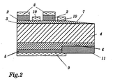
- the means comprise a short circuit region 11 which is connected to the stop layer 6 and short circuits it to the anode 9.
- the doping of the short-circuit region 11 must at least compensate for the doping of the anode emitter 5, ie the short-circuit region will generally be doped n +.
- the blocking structure in the region of the edge termination 7 is thus a diode. This eliminates the gain of the reverse current in this area. The thermal load in the edge area is thus reduced. As a result, the operating temperature can be increased at a predetermined voltage.
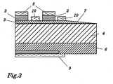
- FIG. 3 shows another solution.
- the anode emitter 5 is not executed over the entire surface, so that the stop layer 6 penetrates to the anode-side main surface and is contacted by the anode 9.
- the stop layer 6 is short-circuited to the anode 9.
- the short circuit can for example take place simultaneously with the formation of the cathode-side emitter.
- the GTO according to the invention is in particular in Its edge termination area thermally stable and can be safely operated in any operating condition.
Landscapes
- Thyristors (AREA)
Description
- Die Erfindung bezieht sich auf das Gebiet der Leistungshalbleitertechnologie. Sie geht aus von einem Abschaltthyristor oder GTO gemäss dem Oberbegriff des ersten Anspruchs.
- Ein solcher GTO umfasst im wesentlichen eine npnp Vierschichtstruktur sowie eine anodenseitige Stopschicht und wird zum Beispiel in der Deutschen Offenlegungsschriften
DE 43 13 170 A1 beschrieben. Weitere GTOs mit Stopschicht sind aus dem US PatentUS 5,028,974 und derDE 44 31 294 A1 bekannt. - Abschaltbare Thyristoren mit Stoppschicht und homogenem Anodenemitter mit geringer fizienz, wie zum Beispiel in der genannten
DE 43 13 170 A1 offenbart, werden üblicherweise mit ganzflächiger Stopschicht und ganzflächigem Anodenemitter hergestellt. Im blockierenden Zustand fliesst dann ein gewisser Sperrstrom zwischen Anode und Gate eines solchen Elementes. In der Raumladungszone werden Ladungsträger erzeugt. Die so entstandenen Löcher fliessen durch den Gateanschluss ab, die Elektronen durch die Anode. Bei ganzflächiger Ausführung von Stopschicht und Anodenemitter stellt der sperrende GTO somit einen Transistor mit offener Basis dar. Die durch die Anode abfliessenden Elektronen führen zu einem Spannungsabfall am Anodenemitter. Dies wiederum führt zu einer Injektion von Löchern. Dadurch wird der in der Raumladungszone generierte Sperrstrom zusätzlich verstärkt. - Der Sperrstrom führt zu einer Erwärmung des GTOs. Im Bereich des Randabschlusses ist die Kühlung der Siliziumscheibe aber reduziert. Dadurch kann es in diesem Bereich zu einem unkontrollierten Anstieg der Temperatur kommen. Dies führt zu einem weiteren Anstieg des Sperrstromes. Insgesamt kann die beschriebene Problematik zu einem thermischen Weglaufen und schlimmstenfalls zu einer Zerstörung des Elementes führen.
- Das Dokument
JP 62-1273 -
JP 60-154564 - Aufgabe der Erfindung ist es deshalb, einen Abschaltthyristor (GTO) anzugeben, der insbesondere in seinem Randabschlussgebiet thermisch stabil ist und in jedem Betriebszustand sicher betrieben werden kann. Diese Aufgabe wird durch die Merkmale des unabhängigen Anspruchs gelöst.
- Kern der Erfindung ist es also, im Bereich des Randabschlusses Mittel vorgesehen sind, die die Stopschicht mit der Anode verbinden. Dadurch weist der GTO im sperrenden Zustand im Randbereich die Struktur einer Diode auf, und die eingangs beschriebene Verstärkung des Sperrstromes fällt weg. Die thermische Belastung im Randbereich wird reduziert, und das Bauelement erträgt bei vorgegebener Spannung eine höhere Betriebstemperatur.
- Ein erstes Ausführungsbeispiel ist dadurch gekennzeichnet, dass im Bereich des Randabschlusses ein Kurzschlussgebiet vorgesehen ist, das mit der Anode verbunden ist und die Stopschicht mit der Anode kurzschliesst. In einem zweiten Ausführungsbeispiel ist der Anodenemitter nicht ganzflächig ausgebildet, sondern er wird im Bereich des Randabschlusses durch die mit der Anode verbundene Stopschicht ersetzt.
- Nachfolgend wird die Erfindung anhand von Ausführungsbeispielen im Zusammenhang mit den Zeichnungen näher erläutert.
- Es zeigen:
- Fig. 1
- Ein GTO mit anodenseitiger Stopschicht nach dem Stand der Technik;
- Fig. 2
- Ein erfindungsgemässer GTO nach einem ersten Ausführungsbeispiel;
- Fig. 3
- Ein erfindungsgemässer GTO nach einem zweiten Ausführungsbeispiel.
- Die in den Zeichnungen verwendeten Bezugszeichen und deren Bedeutung sind in der Bezugszeichenliste zusammengefasst aufgelistet. Grundsätzlich sind in den Figuren gleiche Teile mit gleichen Bezugszeichen versehen.
- In
Figur 1 ist ein Ausschnitt eines Abschaltthyristors oder GTOs nach dem Stand der Technik dargestellt. In einem Halbleiterkörper 1 ist eine Anzahl von unterschiedlich dotierten Schichten, die im wesentlichen eine npnp-Thyristorstruktur bilden, angeordnet. N-dotierte Gebiete sind mit von oben rechts nach unten links verlaufenden Linien schraffiert, p-dotierte Gebiete mit von oben links nach unten rechts verlaufenden Linien und Metallisierungen mit waagrechten kurzen Strichen. Die Dichte der Schraffur kann als Hinweis auf die Dotierungsstärke verstanden werden. Von einer anodenseitigen Hauptfläche her folgen ein p+ dotierter Anodenemitter 5, eine n dotierte Stopschicht 6, eine n- dotierte n-Basis 4, eine p dotierte p-Basis 3 und n+ dotierte Kathodenemittergebiete 2. Die letzteren werden von einer eine Kathode 8 bildenden Metallisierung kontaktiert. Die Kathodenemittergebiete 2 können wie dargestellt erhaben oder aber auch in die p-Basis 3 integriert ausgeführt sein. Zwischen den Kathodenemittergebieten 2 wird die p-Basis 3 von einer ein Gate 10 bildenden Metallisierungen kontaktiert. Um Feldüberhöhungen am Rand des GTO zu vermeiden und das Bauelement sicher für hohe Spannungen zu machen ist randseitig ein sog. Randabschlussgebiet 7 vorgesehen. Wie in der Figur gezeigt, weist das Randabschlussgebiet kathodenseitig keine elektrische Kontaktierung auf. In diesem Bereich sind keine Kathodenemitter 2 mehr vorhanden und die Halbleiterscheibe kann insbesondere abgeschrägt sein. - Solche Abschaltthyristoren mit einer Stopschicht 6 und einem homogenen Anodenemitter 5 werden heute hergestellt mit einer ganzflächigen Stopschicht 6 und einem ganzflächigem Anodenemitter 5. Vorzugsweise weist der Anodenemitter 5 ausserdem eine geringe Effizienz auf. Im blockierenden Zustand fliesst dann ein gewisser Sperrstrom zwischen Anode und Gate eines solchen Elementes. In der Raumladungszone werden Ladungsträger erzeugt. Die so entstandenen Löcher fliessen durch den Gateanschluss ab, die Elektronen durch die Anode. Bei ganzflächiger Ausführung von Stopschicht und Anodenemitter stellt der sperrende GTO somit einen Transistor mit offener Basis dar. Die durch die Anode abfliessenden Elektronen führen zu einem Spannungsabfall am Anodenemitter. Dies wiederum führt zu einer Injektion von Löchern. Dadurch wird der in der Raumladungszone generierte Sperrstrom zusätzlich verstärkt.
- Der Sperrstrom führt zu einer Erwärmung des GTOs. Im Bereich des Randabschlusses ist die Kühlung der Siliziumscheibe aber reduziert. Dadurch kann es in diesem Bereich zu einem unkontrollierten Anstieg der Temperatur kommen. Dies führt zu einem weiteren Anstieg des Sperrstromes. Insgesamt kann die beschriebene Problematik zu einem thermischen Weglaufen und schlimmstenfalls zu einer Zerstörung des Elementes führen.
- Nach
Figur 2 und3 werden deshalb nach der Erfindung im Bereich des Randabschlusses Mittel vorgesehen, die die Stopschicht mit der Anode verbinden. Gemäss dem Ausführungsbeispiel nachFigur 2 umfassen die Mittel einen Kurzschlussgebiet 11, das mit der Stopschicht 6 verbunden ist und diese mit der Anode 9 kurzschliesst. Die Dotierung des Kurzschlussgebietes 11 muss die Dotierung des Anodenemitters 5 mindestens kompensieren, d.h. das Kurzschlussgebiet wird im allgemeinen n+ dotiert sein. Die sperrende Struktur im Bereich des Randabschlusses 7 ist somit eine Diode. Dadurch entfällt in diesem Bereich die Verstärkung des Sperrstromes. Die thermische Belastung im Randbereich wird damit reduziert. Demzufolge kann die Betriebstemperatur bei vorgegebener Spannung erhöht werden. -
Figur 3 zeigt eine andere Lösung. Hier wird der Anodenemitter 5 nicht ganzflächig ausgeführt, so dass die Stopschicht 6 bis zur anodenseitigen Hauptfläche dringt und von der Anode 9 kontaktiert wird. Somit wird auch hier die Stopschicht 6 mit der Anode 9 kurzgeschlossen. Der Kurzschluss kann beispielsweise gleichzeitig mit der Ausbildung des kathodenseitigen Emitters erfolgen. Insgesamt ergibt sich mit der Erfindung ein GTO, der thermisch stärker belastet werden kann, somit robuster ist und weniger Kühlung benötigt. Der erfindungsgemässe GTO ist insbesondere in seinem Randabschlussgebiet thermisch stabil und kann in jedem Betriebszustand sicher betrieben werden. -
- 1
- Halbleiterkörper
- 2
- Kathodenemittergebiet
- 3
- p-Basis
- 4
- n-Basis
- 5
- Anodenemitter
- 6
- Stopschicht
- 7
- Randabschlussgebiet
- 8
- Kathode, Kathodenmetallisierung
- 9
- Anode, Anodenmetallisierung
- 10
- Gate
- 11
- n+ Kurzschlussgebiet
Claims (3)
- Abschaltthyristor (GTO) umfassenda) in einem Halbleiterkörper (1) eine npnp-Vierschichtstruktur mit Kathodenemittergebieten (2), einer p-Basis (3), einer n-Basis (4) und einem homogenen Anodenemitter (5);b) eine stärker als die n-Basis (4) dotierte Stopschicht (6), die zwischen der n-Basis (4) und dem Anodenemitter (5) angeordnet ist;c) eine Kathode (8), die die Kathodenemittergebiete (2) kontaktiert, eine Anode (9), die den Anodenemitter (5) kontaktiert und ein Gate (10), das die p-Basis (3) kontaktiert;d) ein Randabschlussgebiet (7), welches am Rand des Halbleiterkörpers (1) angeordnet ist, welches Randabschlussgebiet (7) Teile der p-Basis (3), der n-Basis (4) und der Stopschicht (6) enthält und welches Randabschlussgebiet (7) kathodenseitig keine elektrische Kontaktierung aufweist und an der kathodenseitigen Oberfläche des Halbleiterkörpers (1) eine Abschrägung aufweist;
dadurch gekennzeichnet, dasse) im Bereich des Randabschlussgebietes (7) Mittel vorgesehen sind, die die Stopschicht (6) mit der Anode (9) verbinden. - GTO nach Anspruch 1, dadurch gekennzeichnet, dass im Bereich des Randabschlussgebietes (7) ein Kurzschlussgebiet (11) vorgesehen ist, das mit der Anode (9) verbunden ist und die Stopschicht (6) mit der Anode (9) kurzschliesst.
- GTO nach Anspruch 1, dadurch gekennzeichnet, dass der Anodenemitter (5) nicht ganzflächig ausgebildet ist und im Bereich des Randabschlussgebietes (7) durch die mit der Anode (9) verbundene Stopschicht (6) ersetzt ist.
Applications Claiming Priority (2)
| Application Number | Priority Date | Filing Date | Title |
|---|---|---|---|
| DE19746974A DE19746974A1 (de) | 1997-10-24 | 1997-10-24 | Abschaltthyristor mit Stopschicht |
| DE19746974 | 1997-10-24 |
Publications (3)
| Publication Number | Publication Date |
|---|---|
| EP0923136A2 EP0923136A2 (de) | 1999-06-16 |
| EP0923136A3 EP0923136A3 (de) | 1999-12-22 |
| EP0923136B1 true EP0923136B1 (de) | 2008-07-02 |
Family
ID=7846472
Family Applications (1)
| Application Number | Title | Priority Date | Filing Date |
|---|---|---|---|
| EP98810788A Expired - Lifetime EP0923136B1 (de) | 1997-10-24 | 1998-08-17 | Abschaltthyristor mit Stopschicht |
Country Status (7)
| Country | Link |
|---|---|
| US (1) | US6107651A (de) |
| EP (1) | EP0923136B1 (de) |
| JP (1) | JPH11191618A (de) |
| CN (1) | CN1126181C (de) |
| DE (2) | DE19746974A1 (de) |
| RU (1) | RU2214650C2 (de) |
| UA (1) | UA61907C2 (de) |
Families Citing this family (2)
| Publication number | Priority date | Publication date | Assignee | Title |
|---|---|---|---|---|
| RU2335824C1 (ru) * | 2007-02-20 | 2008-10-10 | Физико-технический институт им. А.Ф. Иоффе РАН | Запираемый тиристор и способ его работы |
| JP2011249601A (ja) * | 2010-05-27 | 2011-12-08 | Shindengen Electric Mfg Co Ltd | 短絡型サイリスタ |
Citations (1)
| Publication number | Priority date | Publication date | Assignee | Title |
|---|---|---|---|---|
| JPS60154564A (ja) * | 1984-01-24 | 1985-08-14 | Fuji Electric Corp Res & Dev Ltd | 半導体装置 |
Family Cites Families (18)
| Publication number | Priority date | Publication date | Assignee | Title |
|---|---|---|---|---|
| JPS53110386A (en) * | 1977-03-08 | 1978-09-27 | Toshiba Corp | Semiconductor device |
| JPS5372479U (de) * | 1977-08-04 | 1978-06-17 | ||
| JPS6043032B2 (ja) * | 1978-09-14 | 1985-09-26 | 株式会社日立製作所 | ゲートターンオフサイリスタ |
| JPS5665667U (de) * | 1979-10-24 | 1981-06-01 | ||
| DE3109892A1 (de) * | 1981-03-14 | 1982-09-23 | SEMIKRON Gesellschaft für Gleichrichterbau u. Elektronik mbH, 8500 Nürnberg | Rueckwaerts nicht sperrender thyristor mit kurzer freiwerdezeit |
| EP0178387B1 (de) * | 1984-10-19 | 1992-10-07 | BBC Brown Boveri AG | Abschaltbares Leistungshalbleiterbauelement |
| JPS621273A (ja) * | 1985-06-26 | 1987-01-07 | Fuji Electric Co Ltd | 逆導通gtoサイリスタ |
| JP2594278B2 (ja) * | 1986-07-30 | 1997-03-26 | ビービーシー ブラウン ボヴェリ アクチェンゲゼルシャフト | 加圧接続型gtoサイリスタ |
| EP0270975B1 (de) * | 1986-12-01 | 1994-11-09 | Kabushiki Kaisha Toshiba | Halbleiter-Schaltanordnung mit einer Anodenkurzschlussstruktur |
| SU1616450A1 (ru) * | 1988-12-29 | 1994-01-30 | Всесоюзный Электротехнический Институт Им.В.И.Ленина | Силовой запираемый тиристор |
| JP2960506B2 (ja) * | 1990-09-19 | 1999-10-06 | 株式会社日立製作所 | ターンオフ形半導体素子 |
| JPH0661477A (ja) * | 1992-08-10 | 1994-03-04 | Meidensha Corp | 半導体素子および半導体素子の製造方法 |
| DE4313170A1 (de) * | 1993-04-22 | 1994-10-27 | Abb Management Ag | Leistungshalbleiterbauelement |
| JP3214236B2 (ja) * | 1993-06-30 | 2001-10-02 | 株式会社日立製作所 | 半導体装置及び電力変換装置 |
| DE4403429C2 (de) * | 1994-02-04 | 1997-09-18 | Asea Brown Boveri | Abschaltbares Halbleiterbauelement |
| DE4431294A1 (de) * | 1994-09-02 | 1996-03-07 | Abb Management Ag | Abschaltbarer Thyristor für hohe Blockierspannungen und kleiner Bauelementdicke |
| JPH0888351A (ja) * | 1994-09-20 | 1996-04-02 | Meidensha Corp | ゲートターンオフサイリスタ |
| JPH08204172A (ja) * | 1995-01-27 | 1996-08-09 | Hitachi Ltd | 圧接型半導体装置 |
-
1997
- 1997-10-24 DE DE19746974A patent/DE19746974A1/de not_active Withdrawn
-
1998
- 1998-07-30 US US09/124,892 patent/US6107651A/en not_active Expired - Lifetime
- 1998-08-17 EP EP98810788A patent/EP0923136B1/de not_active Expired - Lifetime
- 1998-08-17 DE DE59814248T patent/DE59814248D1/de not_active Expired - Lifetime
- 1998-10-12 JP JP10289618A patent/JPH11191618A/ja active Pending
- 1998-10-23 RU RU98119280/28A patent/RU2214650C2/ru not_active IP Right Cessation
- 1998-10-23 CN CN98123435A patent/CN1126181C/zh not_active Expired - Lifetime
- 1998-10-23 UA UA98105591A patent/UA61907C2/uk unknown
Patent Citations (1)
| Publication number | Priority date | Publication date | Assignee | Title |
|---|---|---|---|---|
| JPS60154564A (ja) * | 1984-01-24 | 1985-08-14 | Fuji Electric Corp Res & Dev Ltd | 半導体装置 |
Also Published As
| Publication number | Publication date |
|---|---|
| CN1215929A (zh) | 1999-05-05 |
| CN1126181C (zh) | 2003-10-29 |
| DE19746974A1 (de) | 1999-04-29 |
| RU2214650C2 (ru) | 2003-10-20 |
| JPH11191618A (ja) | 1999-07-13 |
| UA61907C2 (en) | 2003-12-15 |
| DE59814248D1 (de) | 2008-08-14 |
| EP0923136A2 (de) | 1999-06-16 |
| US6107651A (en) | 2000-08-22 |
| EP0923136A3 (de) | 1999-12-22 |
Similar Documents
| Publication | Publication Date | Title |
|---|---|---|
| DE102005018366B4 (de) | Rückwärtsleitende Halbleitervorrichtung | |
| DE69120995T2 (de) | Hochgeschwindigkeitsdiode und Verfahren zur Herstellung | |
| DE69325608T2 (de) | Halbleiterbauelement mit einem Schutzmittel | |
| EP0360036B1 (de) | Planarer pn-Übergang hoher Spannungsfestigkeit | |
| EP0283496B1 (de) | Halbleiterbauelement mit einer anodenseitigen p-zone und einer anliegenden schwach dotierten n-basiszone | |
| DE102019202108B4 (de) | Halbleitervorrichtung | |
| DE3147075A1 (de) | "halbleitergleichrichtereinrichtung" | |
| EP0913000B1 (de) | Durch feldeffekt steuerbares halbleiterbauelement | |
| EP1097482B1 (de) | J-fet-halbleiteranordnung | |
| WO1999053549A1 (de) | Universal-halbleiterscheibe für hochvolt-halbleiterbauelemente | |
| DE69122902T2 (de) | Halbleiteranordnung mit einem Thyristor | |
| EP0710988B1 (de) | Verfahren zum Herstellen von durch Feldeffekt steuerbaren Halbleiterbauelementen | |
| EP0430133B1 (de) | Leistungs-Halbleiterbauelement mit Emitterkurzschlüssen | |
| DE3888462T2 (de) | Verfahren zur Herstellung einer gegen Überspannungen selbst-geschützten Halbleiteranordnung. | |
| DE19538090A1 (de) | Leistungshalbleiterelement | |
| EP0700095B1 (de) | Abschaltbarer Thyristor für hohe Blockierspannungen und kleiner Bauelementdicke | |
| DE4438896A1 (de) | Halbleiterdiode mit Elektronenspender | |
| EP0206350B1 (de) | Thyristor mit verminderter Mittelzonendicke | |
| DE69500782T2 (de) | Thyristor mit isoliertem Gate | |
| EP0923136B1 (de) | Abschaltthyristor mit Stopschicht | |
| DE69319465T2 (de) | Gate-Turn-Off-Thyristor und dessen Verwendung in Leistungwandlern | |
| EP0651445A2 (de) | Abschaltbarer Thyristor | |
| EP0224757B1 (de) | Rückwärtsleitender Thyristor | |
| DE4342482C2 (de) | Schnelle Leistungshalbleiterbauelemente | |
| EP0889531A1 (de) | MOS gesteuertes Halbleiterbauelement |
Legal Events
| Date | Code | Title | Description |
|---|---|---|---|
| PUAI | Public reference made under article 153(3) epc to a published international application that has entered the european phase |
Free format text: ORIGINAL CODE: 0009012 |
|
| AK | Designated contracting states |
Kind code of ref document: A2 Designated state(s): DE FR GB |
|
| AX | Request for extension of the european patent |
Free format text: AL;LT;LV;MK;RO;SI |
|
| PUAL | Search report despatched |
Free format text: ORIGINAL CODE: 0009013 |
|
| AK | Designated contracting states |
Kind code of ref document: A3 Designated state(s): AT BE CH CY DE DK ES FI FR GB GR IE IT LI LU MC NL PT SE |
|
| AX | Request for extension of the european patent |
Free format text: AL;LT;LV;MK;RO;SI |
|
| RAP1 | Party data changed (applicant data changed or rights of an application transferred) |
Owner name: ABB SEMICONDUCTORS AG |
|
| 17P | Request for examination filed |
Effective date: 20000526 |
|
| AKX | Designation fees paid |
Free format text: DE FR GB |
|
| RAP1 | Party data changed (applicant data changed or rights of an application transferred) |
Owner name: ABB SCHWEIZ AG |
|
| 17Q | First examination report despatched |
Effective date: 20060224 |
|
| GRAP | Despatch of communication of intention to grant a patent |
Free format text: ORIGINAL CODE: EPIDOSNIGR1 |
|
| GRAS | Grant fee paid |
Free format text: ORIGINAL CODE: EPIDOSNIGR3 |
|
| GRAA | (expected) grant |
Free format text: ORIGINAL CODE: 0009210 |
|
| AK | Designated contracting states |
Kind code of ref document: B1 Designated state(s): DE FR GB |
|
| REG | Reference to a national code |
Ref country code: GB Ref legal event code: FG4D Free format text: NOT ENGLISH |
|
| REF | Corresponds to: |
Ref document number: 59814248 Country of ref document: DE Date of ref document: 20080814 Kind code of ref document: P |
|
| PLBE | No opposition filed within time limit |
Free format text: ORIGINAL CODE: 0009261 |
|
| STAA | Information on the status of an ep patent application or granted ep patent |
Free format text: STATUS: NO OPPOSITION FILED WITHIN TIME LIMIT |
|
| 26N | No opposition filed |
Effective date: 20090403 |
|
| REG | Reference to a national code |
Ref country code: FR Ref legal event code: PLFP Year of fee payment: 18 |
|
| PGFP | Annual fee paid to national office [announced via postgrant information from national office to epo] |
Ref country code: FR Payment date: 20150820 Year of fee payment: 18 |
|
| REG | Reference to a national code |
Ref country code: FR Ref legal event code: ST Effective date: 20170428 |
|
| PG25 | Lapsed in a contracting state [announced via postgrant information from national office to epo] |
Ref country code: FR Free format text: LAPSE BECAUSE OF NON-PAYMENT OF DUE FEES Effective date: 20160831 |
|
| PGFP | Annual fee paid to national office [announced via postgrant information from national office to epo] |
Ref country code: GB Payment date: 20170822 Year of fee payment: 20 Ref country code: DE Payment date: 20170822 Year of fee payment: 20 |
|
| REG | Reference to a national code |
Ref country code: DE Ref legal event code: R071 Ref document number: 59814248 Country of ref document: DE |
|
| REG | Reference to a national code |
Ref country code: GB Ref legal event code: PE20 Expiry date: 20180816 |
|
| PG25 | Lapsed in a contracting state [announced via postgrant information from national office to epo] |
Ref country code: GB Free format text: LAPSE BECAUSE OF EXPIRATION OF PROTECTION Effective date: 20180816 |