EP0923136A2 - Abschaltthyristor mit Stopschicht - Google Patents
Abschaltthyristor mit Stopschicht Download PDFInfo
- Publication number
- EP0923136A2 EP0923136A2 EP98810788A EP98810788A EP0923136A2 EP 0923136 A2 EP0923136 A2 EP 0923136A2 EP 98810788 A EP98810788 A EP 98810788A EP 98810788 A EP98810788 A EP 98810788A EP 0923136 A2 EP0923136 A2 EP 0923136A2
- Authority
- EP
- European Patent Office
- Prior art keywords
- anode
- stop layer
- area
- gto
- emitter
- Prior art date
- Legal status (The legal status is an assumption and is not a legal conclusion. Google has not performed a legal analysis and makes no representation as to the accuracy of the status listed.)
- Granted
Links
Images

Classifications
-
- H—ELECTRICITY
- H10—SEMICONDUCTOR DEVICES; ELECTRIC SOLID-STATE DEVICES NOT OTHERWISE PROVIDED FOR
- H10D—INORGANIC ELECTRIC SEMICONDUCTOR DEVICES
- H10D62/00—Semiconductor bodies, or regions thereof, of devices having potential barriers
- H10D62/10—Shapes, relative sizes or dispositions of the regions of the semiconductor bodies; Shapes of the semiconductor bodies
- H10D62/13—Semiconductor regions connected to electrodes carrying current to be rectified, amplified or switched, e.g. source or drain regions
- H10D62/141—Anode or cathode regions of thyristors; Collector or emitter regions of gated bipolar-mode devices, e.g. of IGBTs
- H10D62/142—Anode regions of thyristors or collector regions of gated bipolar-mode devices
-
- H—ELECTRICITY
- H10—SEMICONDUCTOR DEVICES; ELECTRIC SOLID-STATE DEVICES NOT OTHERWISE PROVIDED FOR
- H10D—INORGANIC ELECTRIC SEMICONDUCTOR DEVICES
- H10D18/00—Thyristors
- H10D18/60—Gate-turn-off devices
-
- H—ELECTRICITY
- H10—SEMICONDUCTOR DEVICES; ELECTRIC SOLID-STATE DEVICES NOT OTHERWISE PROVIDED FOR
- H10D—INORGANIC ELECTRIC SEMICONDUCTOR DEVICES
- H10D62/00—Semiconductor bodies, or regions thereof, of devices having potential barriers
- H10D62/10—Shapes, relative sizes or dispositions of the regions of the semiconductor bodies; Shapes of the semiconductor bodies
- H10D62/13—Semiconductor regions connected to electrodes carrying current to be rectified, amplified or switched, e.g. source or drain regions
- H10D62/141—Anode or cathode regions of thyristors; Collector or emitter regions of gated bipolar-mode devices, e.g. of IGBTs
- H10D62/148—Cathode regions of thyristors
Definitions
- the invention relates to the field of power semiconductor technology. It is based on a shutdown thyristor or GTO according to the generic term of the first Claim.
- Such a GTO essentially comprises an npnp four-layer structure and one stop layer on the anode side and is used, for example, in German Offenlegungsschriften DE 43 13 170 A1 described.
- Other GTOs with a stop layer are from the US Patent US 5,028,974 and DE 44 31 294 A1 are known.
- Switchable thyristors with stop layer and homogeneous anode emitter with low Efficiency as disclosed for example in the aforementioned DE 43 13 170 A1 usually with full-surface stop layer and full-surface anode emitter manufactured.
- a certain reverse current then flows between Anode and gate of such an element. Charge carriers become in the space charge zone generated. The holes created in this way flow through the gate connection off, the electrons through the anode.
- the blocking GTO With full-surface execution of stop layer and anode emitter, the blocking GTO thus provides an open base transistor The electrons flowing through the anode lead to a voltage drop at the anode emitter. This in turn leads to an injection of holes. Thereby the reverse current generated in the space charge zone is additionally amplified.
- the reverse current causes the GTO to heat up. In the area of the edging the cooling of the silicon wafer is reduced. This allows it in this Range to an uncontrolled increase in temperature. this leads to a further increase in reverse current. Overall, the problem described can thermal runaway and, at worst, destruction of the element.
- the object of the invention is therefore to provide a shutdown thyristor (GTO) is thermally stable, particularly in its edge termination area, and in any operating state can be operated safely. This task is due to the characteristics of independent claims.
- GTO shutdown thyristor
- the essence of the invention is therefore to provide means in the area of the edge closure that connect the stop layer to the anode.
- the GTO points in the blocking State in the edge area on the structure of a diode, and the one described at the beginning
- the amplification of the reverse current is eliminated.
- the thermal load in the The edge area is reduced and the component can withstand a given voltage a higher operating temperature.
- a first exemplary embodiment is characterized in that in the region of the A short-circuit area is provided at the edge, which is connected to the anode and short-circuits the stop layer with the anode.
- the anode emitter is not formed over the entire surface, but rather is in the area of the edge termination through the stop layer connected to the anode replaced.
- FIG. 1 shows a section of a switch-off thyristor or GTO according to the prior art Technology shown.
- a number of is different in a semiconductor body 1 doped layers which essentially form an npnp thyristor structure. N-doped regions are from top right to bottom left Hatched lines, p-doped areas with areas from top left to bottom right Lines and metallizations with short horizontal lines. The concentration the hatching can be understood as an indication of the doping strength.
- a p + doped anode emitter 5 From a main surface on the anode side is followed by a p + doped anode emitter 5, a n doped stop layer 6, an n-doped n-base 4, a p-doped p-base 3 and n + doped cathode emitter regions 2.
- the latter are from a cathode 8 forming metallization contacted.
- the cathode emitter regions 2 can be like shown raised or be integrated into the p-base 3.
- the p base 3 is formed by a gate 10 Metallizations contacted.
- edge termination area 7 To field overflows at the edge of the GTO avoid and make the component safe for high voltages is on the edge a so-called edge termination area 7 is provided. There are no cathode emitters in this area 2 more available and the semiconductor wafer can in particular beveled be.
- Such turn-off thyristors with a stop layer 6 and a homogeneous anode emitter 5 are manufactured today with a full-surface stop layer 6 and one full-surface anode emitter 5.
- the anode emitter 5 also has low efficiency.
- a certain one then flows in the blocking state Reverse current between anode and gate of such an element. In the space charge zone charge carriers are generated. The resulting holes flow through the gate connection, the electrons through the anode.
- the blocking GTO thus provides the execution of the stop layer and anode emitter Open base transistor.
- the electrons flowing through the anode lead to a voltage drop at the anode emitter. This in turn leads to a Injection of holes. This causes the reverse current generated in the space charge zone additionally reinforced.
- the reverse current causes the GTO to heat up. In the area of the edging the cooling of the silicon wafer is reduced. This allows it in this Range to an uncontrolled increase in temperature. this leads to a further increase in reverse current. Overall, the problem described can thermal runaway and, at worst, destruction of the element.
- the edge termination Means are provided which connect the stop layer to the anode.
- the means comprise a short-circuit area 11, which is connected to the stop layer 6 and this short-circuits with the anode 9.
- the doping of the short-circuit region 11 must be the doping of the anode emitter 5 at least compensate, i.e. the short-circuit area is generally n + doped be.
- the locking structure in the area of the edge closure 7 is therefore one Diode. This eliminates the amplification of the reverse current in this area. The This reduces thermal stress in the edge area. As a result, the Operating temperature can be increased at a given voltage.
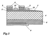
- Figure 3 shows another solution.
- the anode emitter 5 does not cover the entire surface executed so that the stop layer 6 penetrates to the anode-side main surface and is contacted by the anode 9.
- the stop layer 6 with the Anode 9 shorted.
- the short circuit can, for example, coincide with the Formation of the cathode-side emitter take place.
- the GTO according to the invention is in particular in its edge termination area is thermally stable and safe in any operating condition operate.
Landscapes
- Thyristors (AREA)
Abstract
Description
- Fig. 1
- Ein GTO mit anodenseitiger Stopschicht nach dem Stand der Technik;
- Fig. 2
- Ein erfindungsgemässer GTO nach einem ersten Ausführungsbeispiel;
- Fig. 3
- Ein erfindungsgemässer GTO nach einem zweiten Ausführungsbeispiel.
- 1
- Halbleiterkörper
- 2
- Kathodenemittergebiet
- 3
- p-Basis
- 4
- n-Basis
- 5
- Anodenemitter
- 6
- Stopschicht
- 7
- Randabschlussgebiet
- 8
- Kathode, Kathodenmetallisierung
- 9
- Anode, Anodenmetallisierung
- 10
- Gate
- 11
- n+ Kurzschlussgebiet
Claims (3)
- Abschaltthyristor (GTO) umfassenda) in einem Halbleiterkörper (1) eine npnp-Vierschichtstruktur mit Kathodenemittergebieten (2), einer p-Basis (3), einer n-Basis (4) und einem homogenen Anodenemitter (5);b) eine stärker als die n-Basis (4) dotierte Stopschicht (6), die zwischen der n-Basis (4) und dem Anodenemitter (5) angeordnet ist;c) ein Randabschlussgebiet (7), dass keine Kathodenemittergebiete und insbesondere eine Abschrägung aufweist;d) ein Kathode (8), die die Kathodenemittergebiete (2) kontaktiert, eine Anode (9), die den Anodenemitter (5) kontaktiert und ein Gate (10), das mit die p-Basis (3) kontaktiert;dadurch gekennzeichnet, dasse) im Bereich des Randabschlussgebietes (7) Mittel vorgesehen sind, die die Stopschicht (6) mit der Anode (5) verbinden.
- GTO nach Anspruch 1, dadurch gekennzeichnet, dass im Bereich des Randabschlussgebietes (7) ein Kurzschlussgebiet (11) vorgesehen ist, das mit der Anode (9) verbunden ist und die Stopschicht (6) mit der Anode (9) kurzschliesst.
- GTO nach Anspruch 1, dadurch gekennzeichnet, dass der Anodenemitter (5) nicht ganzflächig ausgebildet ist und im Bereich des Randabschlussgebietes (7) durch die mit der Anode (9) verbundene Stopschicht (6) ersetzt ist.
Applications Claiming Priority (2)
| Application Number | Priority Date | Filing Date | Title |
|---|---|---|---|
| DE19746974A DE19746974A1 (de) | 1997-10-24 | 1997-10-24 | Abschaltthyristor mit Stopschicht |
| DE19746974 | 1997-10-24 |
Publications (3)
| Publication Number | Publication Date |
|---|---|
| EP0923136A2 true EP0923136A2 (de) | 1999-06-16 |
| EP0923136A3 EP0923136A3 (de) | 1999-12-22 |
| EP0923136B1 EP0923136B1 (de) | 2008-07-02 |
Family
ID=7846472
Family Applications (1)
| Application Number | Title | Priority Date | Filing Date |
|---|---|---|---|
| EP98810788A Expired - Lifetime EP0923136B1 (de) | 1997-10-24 | 1998-08-17 | Abschaltthyristor mit Stopschicht |
Country Status (7)
| Country | Link |
|---|---|
| US (1) | US6107651A (de) |
| EP (1) | EP0923136B1 (de) |
| JP (1) | JPH11191618A (de) |
| CN (1) | CN1126181C (de) |
| DE (2) | DE19746974A1 (de) |
| RU (1) | RU2214650C2 (de) |
| UA (1) | UA61907C2 (de) |
Families Citing this family (2)
| Publication number | Priority date | Publication date | Assignee | Title |
|---|---|---|---|---|
| RU2335824C1 (ru) * | 2007-02-20 | 2008-10-10 | Физико-технический институт им. А.Ф. Иоффе РАН | Запираемый тиристор и способ его работы |
| JP2011249601A (ja) * | 2010-05-27 | 2011-12-08 | Shindengen Electric Mfg Co Ltd | 短絡型サイリスタ |
Family Cites Families (19)
| Publication number | Priority date | Publication date | Assignee | Title |
|---|---|---|---|---|
| JPS53110386A (en) * | 1977-03-08 | 1978-09-27 | Toshiba Corp | Semiconductor device |
| JPS5372479U (de) * | 1977-08-04 | 1978-06-17 | ||
| JPS6043032B2 (ja) * | 1978-09-14 | 1985-09-26 | 株式会社日立製作所 | ゲートターンオフサイリスタ |
| JPS5665667U (de) * | 1979-10-24 | 1981-06-01 | ||
| DE3109892A1 (de) * | 1981-03-14 | 1982-09-23 | SEMIKRON Gesellschaft für Gleichrichterbau u. Elektronik mbH, 8500 Nürnberg | Rueckwaerts nicht sperrender thyristor mit kurzer freiwerdezeit |
| JPS60154564A (ja) * | 1984-01-24 | 1985-08-14 | Fuji Electric Corp Res & Dev Ltd | 半導体装置 |
| EP0178387B1 (de) * | 1984-10-19 | 1992-10-07 | BBC Brown Boveri AG | Abschaltbares Leistungshalbleiterbauelement |
| JPS621273A (ja) * | 1985-06-26 | 1987-01-07 | Fuji Electric Co Ltd | 逆導通gtoサイリスタ |
| JP2594278B2 (ja) * | 1986-07-30 | 1997-03-26 | ビービーシー ブラウン ボヴェリ アクチェンゲゼルシャフト | 加圧接続型gtoサイリスタ |
| EP0270975B1 (de) * | 1986-12-01 | 1994-11-09 | Kabushiki Kaisha Toshiba | Halbleiter-Schaltanordnung mit einer Anodenkurzschlussstruktur |
| SU1616450A1 (ru) * | 1988-12-29 | 1994-01-30 | Всесоюзный Электротехнический Институт Им.В.И.Ленина | Силовой запираемый тиристор |
| JP2960506B2 (ja) * | 1990-09-19 | 1999-10-06 | 株式会社日立製作所 | ターンオフ形半導体素子 |
| JPH0661477A (ja) * | 1992-08-10 | 1994-03-04 | Meidensha Corp | 半導体素子および半導体素子の製造方法 |
| DE4313170A1 (de) * | 1993-04-22 | 1994-10-27 | Abb Management Ag | Leistungshalbleiterbauelement |
| JP3214236B2 (ja) * | 1993-06-30 | 2001-10-02 | 株式会社日立製作所 | 半導体装置及び電力変換装置 |
| DE4403429C2 (de) * | 1994-02-04 | 1997-09-18 | Asea Brown Boveri | Abschaltbares Halbleiterbauelement |
| DE4431294A1 (de) * | 1994-09-02 | 1996-03-07 | Abb Management Ag | Abschaltbarer Thyristor für hohe Blockierspannungen und kleiner Bauelementdicke |
| JPH0888351A (ja) * | 1994-09-20 | 1996-04-02 | Meidensha Corp | ゲートターンオフサイリスタ |
| JPH08204172A (ja) * | 1995-01-27 | 1996-08-09 | Hitachi Ltd | 圧接型半導体装置 |
-
1997
- 1997-10-24 DE DE19746974A patent/DE19746974A1/de not_active Withdrawn
-
1998
- 1998-07-30 US US09/124,892 patent/US6107651A/en not_active Expired - Lifetime
- 1998-08-17 EP EP98810788A patent/EP0923136B1/de not_active Expired - Lifetime
- 1998-08-17 DE DE59814248T patent/DE59814248D1/de not_active Expired - Lifetime
- 1998-10-12 JP JP10289618A patent/JPH11191618A/ja active Pending
- 1998-10-23 RU RU98119280/28A patent/RU2214650C2/ru not_active IP Right Cessation
- 1998-10-23 CN CN98123435A patent/CN1126181C/zh not_active Expired - Lifetime
- 1998-10-23 UA UA98105591A patent/UA61907C2/uk unknown
Also Published As
| Publication number | Publication date |
|---|---|
| EP0923136B1 (de) | 2008-07-02 |
| CN1215929A (zh) | 1999-05-05 |
| CN1126181C (zh) | 2003-10-29 |
| DE19746974A1 (de) | 1999-04-29 |
| RU2214650C2 (ru) | 2003-10-20 |
| JPH11191618A (ja) | 1999-07-13 |
| UA61907C2 (en) | 2003-12-15 |
| DE59814248D1 (de) | 2008-08-14 |
| US6107651A (en) | 2000-08-22 |
| EP0923136A3 (de) | 1999-12-22 |
Similar Documents
| Publication | Publication Date | Title |
|---|---|---|
| DE19811297B4 (de) | MOS-Halbleitervorrichtung mit hoher Durchbruchspannung | |
| DE102005018366B4 (de) | Rückwärtsleitende Halbleitervorrichtung | |
| EP0621640B1 (de) | Leistungshalbleiterbauelement | |
| DE112017005529B4 (de) | Siliciumcarbid-halbleitereinheit und leistungswandlereinheit | |
| DE112019000291T5 (de) | Halbleiterbauteil und Leistungsmodul | |
| DE102005021249B4 (de) | Halbleitervorrichtung | |
| DE102018200136B4 (de) | Halbleitervorrichtung | |
| DE19816448C1 (de) | Universal-Halbleiterscheibe für Hochspannungs-Halbleiterbauelemente, ihr Herstellungsverfahren und ihre Verwendung | |
| EP1097482B1 (de) | J-fet-halbleiteranordnung | |
| DE112018006467T5 (de) | Siliciumcarbid-halbleiteranordnung und leistungswandler | |
| EP0430133B1 (de) | Leistungs-Halbleiterbauelement mit Emitterkurzschlüssen | |
| EP0768717A2 (de) | Leistungshalbleiterelement | |
| EP0487869B1 (de) | Abschaltbares Leistungshalbleiter-Bauelement | |
| EP0709899A2 (de) | Halbleiterdiode mit Elektronen-Injektionsmittel | |
| EP0651445A2 (de) | Abschaltbarer Thyristor | |
| DE69319465T2 (de) | Gate-Turn-Off-Thyristor und dessen Verwendung in Leistungwandlern | |
| DE102018114375A1 (de) | Leistungselektronikanordnung | |
| EP0206350B1 (de) | Thyristor mit verminderter Mittelzonendicke | |
| DE112014006158T5 (de) | Leistungshalbleitervorrichtung | |
| EP0923136B1 (de) | Abschaltthyristor mit Stopschicht | |
| EP0017980A1 (de) | Thyristor mit Steuerung durch Feldeffekttransistor | |
| EP0224757B1 (de) | Rückwärtsleitender Thyristor | |
| DE102005019860B4 (de) | Steuerbare Halbleiterdiode, elektronisches Bauteil und Spannungszwischenkreisumrichter | |
| DE112022007612T5 (de) | Halbleitereinrichtung und Stromrichtereinrichtung | |
| EP0889531A1 (de) | MOS gesteuertes Halbleiterbauelement |
Legal Events
| Date | Code | Title | Description |
|---|---|---|---|
| PUAI | Public reference made under article 153(3) epc to a published international application that has entered the european phase |
Free format text: ORIGINAL CODE: 0009012 |
|
| AK | Designated contracting states |
Kind code of ref document: A2 Designated state(s): DE FR GB |
|
| AX | Request for extension of the european patent |
Free format text: AL;LT;LV;MK;RO;SI |
|
| PUAL | Search report despatched |
Free format text: ORIGINAL CODE: 0009013 |
|
| AK | Designated contracting states |
Kind code of ref document: A3 Designated state(s): AT BE CH CY DE DK ES FI FR GB GR IE IT LI LU MC NL PT SE |
|
| AX | Request for extension of the european patent |
Free format text: AL;LT;LV;MK;RO;SI |
|
| RAP1 | Party data changed (applicant data changed or rights of an application transferred) |
Owner name: ABB SEMICONDUCTORS AG |
|
| 17P | Request for examination filed |
Effective date: 20000526 |
|
| AKX | Designation fees paid |
Free format text: DE FR GB |
|
| RAP1 | Party data changed (applicant data changed or rights of an application transferred) |
Owner name: ABB SCHWEIZ AG |
|
| 17Q | First examination report despatched |
Effective date: 20060224 |
|
| GRAP | Despatch of communication of intention to grant a patent |
Free format text: ORIGINAL CODE: EPIDOSNIGR1 |
|
| GRAS | Grant fee paid |
Free format text: ORIGINAL CODE: EPIDOSNIGR3 |
|
| GRAA | (expected) grant |
Free format text: ORIGINAL CODE: 0009210 |
|
| AK | Designated contracting states |
Kind code of ref document: B1 Designated state(s): DE FR GB |
|
| REG | Reference to a national code |
Ref country code: GB Ref legal event code: FG4D Free format text: NOT ENGLISH |
|
| REF | Corresponds to: |
Ref document number: 59814248 Country of ref document: DE Date of ref document: 20080814 Kind code of ref document: P |
|
| PLBE | No opposition filed within time limit |
Free format text: ORIGINAL CODE: 0009261 |
|
| STAA | Information on the status of an ep patent application or granted ep patent |
Free format text: STATUS: NO OPPOSITION FILED WITHIN TIME LIMIT |
|
| 26N | No opposition filed |
Effective date: 20090403 |
|
| REG | Reference to a national code |
Ref country code: FR Ref legal event code: PLFP Year of fee payment: 18 |
|
| PGFP | Annual fee paid to national office [announced via postgrant information from national office to epo] |
Ref country code: FR Payment date: 20150820 Year of fee payment: 18 |
|
| REG | Reference to a national code |
Ref country code: FR Ref legal event code: ST Effective date: 20170428 |
|
| PG25 | Lapsed in a contracting state [announced via postgrant information from national office to epo] |
Ref country code: FR Free format text: LAPSE BECAUSE OF NON-PAYMENT OF DUE FEES Effective date: 20160831 |
|
| PGFP | Annual fee paid to national office [announced via postgrant information from national office to epo] |
Ref country code: GB Payment date: 20170822 Year of fee payment: 20 Ref country code: DE Payment date: 20170822 Year of fee payment: 20 |
|
| REG | Reference to a national code |
Ref country code: DE Ref legal event code: R071 Ref document number: 59814248 Country of ref document: DE |
|
| REG | Reference to a national code |
Ref country code: GB Ref legal event code: PE20 Expiry date: 20180816 |
|
| PG25 | Lapsed in a contracting state [announced via postgrant information from national office to epo] |
Ref country code: GB Free format text: LAPSE BECAUSE OF EXPIRATION OF PROTECTION Effective date: 20180816 |