EP0923132B1 - Semiconductor device - Google Patents
Semiconductor device Download PDFInfo
- Publication number
- EP0923132B1 EP0923132B1 EP98107063A EP98107063A EP0923132B1 EP 0923132 B1 EP0923132 B1 EP 0923132B1 EP 98107063 A EP98107063 A EP 98107063A EP 98107063 A EP98107063 A EP 98107063A EP 0923132 B1 EP0923132 B1 EP 0923132B1
- Authority
- EP
- European Patent Office
- Prior art keywords
- node
- signal
- discharge element
- power supply
- signal terminal
- Prior art date
- Legal status (The legal status is an assumption and is not a legal conclusion. Google has not performed a legal analysis and makes no representation as to the accuracy of the status listed.)
- Expired - Lifetime
Links
Images


Classifications
-
- H—ELECTRICITY
- H10—SEMICONDUCTOR DEVICES; ELECTRIC SOLID-STATE DEVICES NOT OTHERWISE PROVIDED FOR
- H10D—INORGANIC ELECTRIC SEMICONDUCTOR DEVICES
- H10D89/00—Aspects of integrated devices not covered by groups H10D84/00 - H10D88/00
- H10D89/60—Integrated devices comprising arrangements for electrical or thermal protection, e.g. protection circuits against electrostatic discharge [ESD]
- H10D89/601—Integrated devices comprising arrangements for electrical or thermal protection, e.g. protection circuits against electrostatic discharge [ESD] for devices having insulated gate electrodes, e.g. for IGFETs or IGBTs
- H10D89/811—Integrated devices comprising arrangements for electrical or thermal protection, e.g. protection circuits against electrostatic discharge [ESD] for devices having insulated gate electrodes, e.g. for IGFETs or IGBTs using FETs as protective elements
-
- H—ELECTRICITY
- H10—SEMICONDUCTOR DEVICES; ELECTRIC SOLID-STATE DEVICES NOT OTHERWISE PROVIDED FOR
- H10D—INORGANIC ELECTRIC SEMICONDUCTOR DEVICES
- H10D86/00—Integrated devices formed in or on insulating or conducting substrates, e.g. formed in silicon-on-insulator [SOI] substrates or on stainless steel or glass substrates
- H10D86/201—Integrated devices formed in or on insulating or conducting substrates, e.g. formed in silicon-on-insulator [SOI] substrates or on stainless steel or glass substrates the substrates comprising an insulating layer on a semiconductor body, e.g. SOI
-
- H—ELECTRICITY
- H10—SEMICONDUCTOR DEVICES; ELECTRIC SOLID-STATE DEVICES NOT OTHERWISE PROVIDED FOR
- H10D—INORGANIC ELECTRIC SEMICONDUCTOR DEVICES
- H10D89/00—Aspects of integrated devices not covered by groups H10D84/00 - H10D88/00
- H10D89/60—Integrated devices comprising arrangements for electrical or thermal protection, e.g. protection circuits against electrostatic discharge [ESD]
- H10D89/601—Integrated devices comprising arrangements for electrical or thermal protection, e.g. protection circuits against electrostatic discharge [ESD] for devices having insulated gate electrodes, e.g. for IGFETs or IGBTs
Definitions
- the present invention relates to a semiconductor device having a MOS transistor formed on a SOI substrate, and more particularly to an input - output protecting function thereof.
- a surge can be discharged into the substrate through a PN junction.
- SOI Silicon - on - insulator
- a path for transferring the surge does not structurally exist on the substrate because the buried insulation layer is formed.
- a longitudinal discharge path does not exist in a thin film SOI structure in which source and drain regions of a MOS transistor reach a buried oxide film. Consequently, it is structurally necessary to perform a transverse discharge. For this reason, the discharge is transversely performed into a power line and a grounding line through the MOS transistor and a diode.
- Fig. 18 is a circuit diagram showing a structure of an input - output protecting circuit having a SOI structure according to the prior art.
- a resistor 36 (hereinafter referred to as a "protecting resistor") for limiting a rush current is first connected to a signal terminal 30 to delay propagation of a surge voltage to an inside through the signal terminal 30, thereby preventing an excessive current from flowing.
- a PMOS transistor Q31 and an NMOS transistor Q32 are provided in series as discharge elements for transferring electric charges between a power supply (node) 32 and a ground level (node) 33.
- the PMOS transistor Q31 and the NMOS transistor Q32 have gates connected to the power supply 32 and the ground level 33, and drains connected to the other end of the protecting resistor 36 in common, respectively. Accordingly, the PMOS transistor Q31 and the NMOS transistor Q32 are. usually brought into an OFF State.
- a similar semiconductor device is disclosed in DE 196 51 247 A1, however, the gates of the transistors are floating.
- the surge voltage is applied to the signal terminal 30
- the electric charges are quickly discharged into the power supply 32 or the ground level 33 by avalanche breakdown of each of the MOS transistors Q31 and Q32 to protect an internal element 31.
- the other end of the protecting resistor 36 is connected to one of ends of an internal resistor 37, and the internal element 31 is connected to the other end of the internal resistor 37. Consequently, the surge voltage is propagated to the internal element 31 with difficulty.
- Fig. 19 shows an input - output protecting circuit formed by using diodes 38 and 39 as discharge elements in the same manner.
- one of ends of a protecting resistor 36 is first connected to a signal terminal 30 to delay propagation of a surge voltage to an inside through the signal terminal 30, thereby preventing an excessive current from flowing.
- the diodes 38 and 39 are provided in series as discharge elements for transferring electric charges between a power supply 32 and a ground level 33.
- a cathode of the diode 38 is connected to the power supply 32, and an anode of the diode 39 is connected to the ground level 33. Accordingly, the diodes 38 and 39 are connected in reverse directions between the power supply 32 and the ground level 33.
- the surge voltage is applied to the signal terminal 30, the electric charges are quickly discharged into the power supply 32 or the ground level 33 by backward avalanche breakdown of the diodes 38 and 39 or a forward current, thereby protecting an internal element 31. Furthermore, an internal resistor 37 is inserted between the protecting resistor 36 and the internal element 31 to propagate the surge voltage to the internal element 31 with difficulty.
- Fig. 20 shows an inverter circuit acting as one of typical internal circuits.
- a PMOS transistor Q33 and an NMOS transistor Q34 are connected in series between a power supply 32 and a ground level 33.
- the PMOS transistor Q33 and the NMOS transistor Q34 have gates connected to an input signal terminal 82 in common, and drains connected to an output signal terminal 83 in common.
- the input - output protecting circuits having the structures shown in Figs. 18 and 19 are connected to the input signal terminal 82 (an input section of the internal circuit) for the internal circuit shown in Fig. 20, they function as input protecting circuits.
- the same input - output protecting circuits are connected to the output signal terminal 83 (an output section of the internal circuit), they function as output protecting circuits.
- the function and operation of the protecting circuit are the same in the input and output sections. Therefore, the protecting circuit will be hereinafter referred to as an "input - output protecting circuit". If the protecting circuit is used as the output protecting circuit, no resistor is often added thereto.
- Fig. 21 is a plan view showing a planar structure of the MOS input - output protecting circuit shown in Fig. 18, and Fig. 22 is a sectional view taken along the line A - A shown in Fig. 21.
- a thin silicon film 3 acting as a SOI layer is provided on a silicon substrate 1 with a buried oxide film 2 acting as an insulation layer interposed therebetween.
- the thin silicon film 3 is divided into two islands 18A and 18B by an interlayer dielectric film 11.
- Channel formation regions 6 and 6d into which an impurity having a concentration of about 10 17 / cm 3 (p - type in NMOS and n - type in PMOS) is implanted are provided, drain and source regions 7 and 8 into which an impurity having a concentration of about 10 20 / cm 3 (n - type in NMOS and p - type in PMOS) is implanted are provided with the channel formation region 6 interposed therebetween, and drain and source regions 7d and 8d into which an impurity having a concentration of about 10 20 / cm 3 is implanted are provided with the channel formation region 6d interposed therebetween.
- gate electrodes 5 and 5d are formed on the channel formation regions 6 and 6d and a part of each of the drain regions 7 and 7d and the source regions 8 and 8d in the thin silicon film 3 with gate oxide films 4 and 4d interposed therebetween, respectively.
- the NMOS transistor Q32 is formed by the gate oxide film 4, the gate electrode 5, the channel formation region 6, the drain region 7 and the source region 8 in the island 18A
- the PMOS transistor Q31 is formed by the gate oxide film 4d, the gate electrode 5d, the channel formation region 6d, the drain region 7d and the source region 8d in the island 18B.
- the interlayer dielectric film 11 divides the thin silicon film 3 into the islands 18A and 18B and is formed over the whole surface of the thin silicon film 3.
- Contact holes 12A to 12D are provided on the interlayer dielectric film 11 in a part of each of the drain regions 7 and 7d and the source regions 8 and 8d.
- An aluminum wiring 14 is electrically connected to the drain regions 7 and 7d through the contact holes 12A and 12B, an aluminum wiring 13 is electrically connected to the source region 8 through the contact hole 12C, and an aluminum wiring 15 is electrically connected to the source region 8d through the contact hole 12D.
- the aluminum wiring 13 is connected to a ground level 33, the aluminum wiring 14 is connected to an input section 30d, and the aluminum wiring 15 is connected to a power supply 32.
- the input section 30d means a portion to be connected to the other end of the protecting resistor 36 as shown in Fig. 19. In Fig. 21, the interlayer dielectric film 11 is omitted.
- the protecting resistor 36 formed of a gate electrode material and a thin silicon film is provided between the signal terminal 30 and the PMOS transistor Q31 and NMOS transistor Q32 which act as discharge elements, and the internal resistor 37 formed of the gate electrode material and the thin silicon film is provided between the discharge elements Q31 and Q32 and the internal element 31.
- the protecting resistor 36 is usually resistant to a rush current flowing into the discharge elements Q31 and Q32. Therefore, a width of the protecting resistor 36 is made greater than that of the internal resistor 37, thus reducing a current density.
- the gate electrode 5d of the PMOS transistor Q31 is connected to the power supply 32 by a gate potential fixing wiring 40, and the gate electrode 5 of the NMOS transistor Q32 is connected to the ground level 33 by a gate potential fixing wiring 41.
- the PMOS transistor Q31 and the NMOS transistor Q32 are set into an OFF state, respectively.
- a surge generated by static electricity is sent through the signal terminal 30 and is first delayed by the protecting resistor 36 to prevent a great rush current from flowing into the discharge elements Q31 and Q32.
- the surge propagated through the protecting resistor 36 is then discharged quickly into the power supply 32 or the ground level 33 through the discharge elements Q31 and Q32.
- the internal resistor 37 does not function to cause the surge to flow in a direction of the internal element but in a direction of the discharge element.
- the surge propagated through the protecting resistor 36 is applied to a discharge element section. If a positive surge voltage is applied, a junction breaks down between the drain region 7 and the channel formation region 6 of the NMOS transistor Q32 to emit the surge to the ground level 33.
- the PMOS transistor Q31 is forward biased and the surge is emitted to the power supply 32 as well. If a negative surge voltage is applied, a junction breaks down between the drain region 7d and the channel formation region 6d of the PMOS transistor Q31 to emit the surge to the power supply 32 and the NMOS transistor Q32 is forward biased to emit the surge.
- the PMOS transistor Q31 and the NMOS transistor Q32 are set in the OFF state. Therefore, an normal operation signal applied to the signal terminal 30 is propagated to the internal element 31 through the protecting resistor 36 and the internal resistor 37.
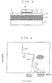
- Fig. 23 is a sectional view showing a sectional structure of the diode type input - output protecting circuit shown in Fig. 19.
- a thin silicon film 3 is provided on a silicon substrate 1 with a buried oxide film 2 acting as an insulation layer interposed therebetween.
- the thin silicon film 3 is divided into two islands 19A and 19B by an interlayer dielectric film 11.
- An anode region 9B into which a p-type impurity having a concentration of about 10 17 / cm 3 is implanted, and a cathode region 10B into which an n-type impurity having a concentration of about 10 17 / cm 3 is implanted are provided, respectively.
- An anode region 9A and a cathode region 10A are provided with the anode region 9B interposed therebetween.
- An anode region 9C and a cathode region 10C are provided with the cathode region 10B interposed therebetween.
- a p-type impurity having a concentration of about 10 20 / cm 3 is implanted into the anode regions 9A and 9C, and an n-type impurity having a concentration of about 10 20 /cm 3 is implanted into the cathode regions 10A and 10C.
- an electrode 5 is formed on the anode region 9B and a part of the anode region 9A and the cathode region 10A in the thin silicon film 3 with an oxide film 4 interposed therebetween, and an electrode 5d is formed on the cathode region 10B and a part of the anode region 9C and the cathode region 10C in the thin silicon film 3 with an oxide film 4d interposed therebetween.
- a diode 39 is formed by the anode regions 9A and 9B and the cathode region 10A.
- a diode 38 is formed by the anode region 9C and the cathode regions 10B and 10C.
- a structure of a diode section is the same as that shown in Fig. 22.
- the anode regions 9B and 9A and the cathode region 10A are replaced with the channel formation region 6, the source region 8 and the drain region 7, respectively.
- the cathode region 10B, the anode region 9C and the cathode region 10C are replaced with the channel formation region 6d, the drain region 7d and the source region 8d, respectively. While the electrodes 5 and 5d are used as masks during formation of the anode regions 9A and 9C and the cathode regions 10A and 10C, they do not function as components of the element
- the next operation of the input - output protecting circuit shown in Figs. 19 and 23 is the same as that of the input - output protecting circuit shown in Figs. 18 and 22 except that emission is performed with breakdown of a junction of the anode region 9B and the cathode region 10A of the diode 39 and breakdown of a junction of the anode region 9C and the cathode region 10B of the diode 38.
- a semiconductor device having an input-output protecting circuit section which includes a signal node connected to a signal terminal and an internal circuit connected to the signal node, which are formed on a SOI substrate.
- the semiconductor device comprises a power supply node and a reference potential node.
- the input-output protection circuit section includes first discharge elements provided between the power supply node and the signal node been forward biased when a surge voltage having a first polarity is applied to the signal terminal. Further discharge elements are provided between the signal node and the reference potential node being forward biased when the surge voltage having a second polarity is applied to the signal terminal.
- the input - output protecting circuit includes the first to fourth discharge elements having PN junctions, each of which is provided between the power supply node or reference potential node and the signal terminal, is reversely biased when the normal operation signal is applied to the signal terminal and is forward biased when the voltage having the first or second polarity is applied to the signal terminal.
- the first and third discharge elements in a forward bias state can cause the power supply node and the reference potential node to discharge a high surge voltage respectively.
- the second and fourth discharge elements in the forward bias state can cause the power supply node and the reference potential node to discharge the surge voltage respectively.
- All the PN junctions of the first to fourth discharge elements are brought into a reverse bias state when the normal operation signal is applied to the signal terminal. Therefore, the normal operation signal does not leak to the power supply node or the grounding line through the first to fourth discharge elements, and normal operation of the internal circuit is not affected by the input - output protecting circuit.
- the input - output protecting circuit is formed by the first and third MOS transistors of the first conductivity type and the second and fourth MOS transistors of the second conductivity type. Two transistors whose conductivity types are different from each other are used, respectively. Therefore, the input - output protecting circuit can easily be manufactured.
- the input - output protecting circuit is formed by the first transistor of the first conductivity type, the second transistor of the second conductivity type, and the first and second diodes. Consequently, the transistors whose conductivity types are different from each other are used one by one. Therefore, the input - output protecting circuit can easily be manufactured.
- the first internal resistor is inserted between the signal terminal and the signal node, and the second internal resistor is inserted between the signal node and the internal circuit. Consequently, if the surge voltage having the first or second polarity is applied to the signal terminal, propagation delay is caused by the first internal resistor and propagation to the internal circuit is prevented by the second internal resistor, thus protecting the internal circuit.
- Fig. 5 is a sectional view showing a SOI structure.
- a buried oxide film 2 is- formed on a silicon substrate 1, and a thin silicon film 3 is formed on the buried oxide film 2.
- a structure comprising the silicon substrate 1, the buried oxide film 2 and the thin silicon film 3 is referred to as a SOI substrate.
- a gate oxide film 4 is selectively formed on the thin silicon film 3.
- a gate electrode 5 is formed on the gate oxide film 4.
- the thin silicon film 3 provided under the gate oxide film 4 acts as a channel formation region 6. Regions in the thin silicon film 3 which are adjacent to the channel formation region 6 act as drain and source regions 7 and 8.
- the buried oxide film 2 having a poor thermal conductivity (which is about 1 / 10 as much as that of silicon) is provided as described above. For this reason, heat generated when a surge voltage is applied is stored so that permanent destruction of a semiconductor device formed on the SOI substrate is easily caused by thermal runaway.
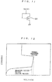
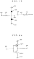
- Fig. 6 is a graph showing a discharge characteristic of an NMOS transistor which is obtained at the time of reverse bias connection.
- the graph of Fig. 6 indicates details of the thermal runaway caused at the time of the reverse bias connection, for example, when an input voltage IN (a surge voltage SV) is applied to a drain of an NMOS transistor Q1 having a source and a gate grounded as shown in Fig. 7.
- a process of the thermal runaway shown in Fig. 6 includes partial processes P1 to P5.
- a drain voltage is quickly raised (P1). Since the NMOS transistor Q1 is reversely biased during the partial process P1, a current hardly flows. When a breakdown induced voltage is reached, the NMOS transistor Q1 causes avalanche breakdown to perform parasitic bipolar operation. Consequently, the drain voltage is dropped up to a holding voltage (P2). Then, the drain voltage is raised again with an internal resistance of the NMOS transistor Q1 (P3).
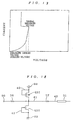
- NMOS transistors In the case where NMOS transistors are usually reversely biased as an input - output protecting circuit on the SOI substrate, NMOS transistors having a channel width W are connected in parallel between an input (voltage) IN and a ground level as shown in Fig. 9.
- six NMOS transistors T1 to T6 having gates grounded are provided in parallel between the input IN and the ground level as shown in Fig. 10.
- the NMOS transistor T1 is formed by a gate electrode 51, a drain region 61 and a source region 71.
- the NMOS transistor T2 is formed by a gate electrode 52, the drain region 61 and a source region 72.
- the NMOS transistor T3 is formed by a gate electrode 53, a drain region 62 and the source region 72.
- the NMOS transistor T4 is formed by a gate electrode 54, the drain region 62 and a source region 73.
- the NMOS transistor T5 is formed by a gate electrode 55, a drain region 63 and the source region 73.
- the NMOS transistor T6 is formed by a gate electrode 56, the drain region 63 and a source region 74.
- a surge voltage is applied from a signal terminal 30.
- the six NMOS transistors T1 to T6 are provided as the input - output protecting circuit on the SOI substrate in parallel between the input IN and the ground level. Consequently, in the case where a current flows between the input IN and the ground level, it splits and flows into the six NMOS transistors T1 to T6.
- Fig. 12 is a graph showing a discharge characteristic of an NMOS transistor which is obtained at the time of forward bias connection.
- the graph of Fig. 12 indicates details of the thermal runaway caused at the time of the forward bias connection, for example, when an input voltage IN (a surge voltage SV) is applied to a drain and a gate of an NMOS transistor Q2 having a source grounded as shown in Fig. 11.
- IN a surge voltage SV
- Fig. 12 is a graph showing the discharge characteristic of the NMOS transistor which is obtained at the time of the forward bias connection in Fig. 11.
- a snap back phenomenon in which a drain voltage is dropped when a breakdown induced voltage is reached is not caused at the time of the forward bias connection.
- a plurality of NMOS transistors T11 to T16 provided in parallel between an input IN and a ground level cause avalanche breakdown almost uniformly with application of the surge voltage SV, and are brought into a thermal runaway state in the same manner as the reverse bias connection when a thermal breakdown voltage is reached by further application of the surge voltage SV.
- Fig. 15 is a graph showing a discharge characteristic of a diode which is obtained at the time of the reverse bias connection.
- the graph of Fig. 15 indicates details of thermal runaway obtained at the time of the reverse bias connection, for example, when the surge voltage SV is applied to a cathode of a diode D1 having an anode grounded as shown in Fig. 14.
- the diode does not perform parasitic bipolar operation. Therefore, a voltage is successively raised after the avalanche breakdown, resulting in thermal breakdown.
- a thermal breakdown voltage which is higher than a breakdown induced voltage is effective in prevention of current concentration in the same manner as in the NMOS transistors which are forward bias connected.
- the breakdown induced voltage itself of the diode is high (which is about twice or three times as much as that of the MOS transistor). Therefore, power dissipation represented by a product of a voltage and a current is increased (that is, heat is also increased). As a result, the ESD resistance is deteriorated. If a junction breakdown voltage of the diode is dropped by a high concentration junction or the like, the breakdown induced voltage can be dropped. Consequently, the ESD resistance can be improved.
- Fig. 17 is a graph showing a discharge characteristic of the diode which is obtained at the time of forward bias connection.
- the graph of Fig. 17 indicates details of thermal runaway caused at the time of the forward bias connection, for example, when a surge voltage SV is applied to an anode of a diode D2 having a cathode grounded as shown in Fig. 16.
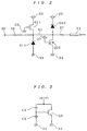
- Fig. 1 is a circuit diagram showing a structure of an input - output protecting circuit according to a first mode of the present invention.
- a signal terminal 30 is connected to one of ends of a protecting resistor 36
- the other end of the protecting resistor 36 is connected to one of ends of an internal resistor 37 through a signal line (signal node) 81
- the other end of the internal resistor 37 is connected to an internal element 31.
- NMOS transistors Q11 and Q12 are connected in series and PMOS transistors Q21 and Q22 are connected in series.
- the NMOS transistor Q11 has a gate connected to the ground level 33, a drain connected to the power supply 32, and a source connected to the other end of the protecting resistor 36 (one of ends of the internal resistor 37).
- the NMOS transistor Q12 has a gate and a source connected to the ground level 33, and a drain connected to the source of the NMOS transistor Q11.
- the PMOS transistor Q21 has a gate and a source connected to the power supply 32, and a drain connected to the other end of the protecting resistor 36.
- the PMOS transistor Q22 has a gate connected to the power supply 32, a source connected to the other end of the protecting resistor 36, and a drain connected to the ground level 33.
- the NMOS transistors Q11 and Q12 and the PMOS transistors Q21 and Q22 may be formed by parallel connection of a plurality of MOS transistors as shown in Figs. 10 and 13.
- a normal operation signal applied to the signal terminal 30 mainly has a voltage ranging from a ground level to a supply level. Therefore, all the NMOS transistors Q11 and Q12 and the PMOS transistors Q21 and Q22 are reversely biased and brought into an OFF state.
- the normal operation signal is sent to the internal element 31 through the protecting resistor 36 and the internal resistor 37 without a leakage to the power supply 32 or the ground level 33 through the MOS transistor Q11, Q12, Q21 or Q22.
- the voltage of the normal operation signal is limited to the range from the ground level to the power level, the NMOS transistors Q11 and Q12 and the PMOS transistors Q21 and Q22 are surely turned off.
- the NMOS transistors Q11 and Q12 and the PMOS transistors Q21 and Q22 are connected so as to be brought into a reverse bias state when the normal operation signal is input to the signal terminal 30. Therefore, the normal operation is not affected.
- the input - output protecting circuit uses two P-channel MOS transistors and two N-channel MOS transistors. As shown in Fig. 20, CMOS inverters including PMOS and NMOS transistors are often formed as the internal element 31. By changing structures of two CMOS inverters a little, the input - output protecting circuit according to the first mode can easily be manufactured.
- the following structure may be used. More specifically, the NMOS transistor Q12 and the PMOS transistor Q21 are replaced with diodes D11 and D12, a cathode of the diode D11 is connected to the other end of the protecting resistor 36 and an anode of the diode D11 is connected to the ground level 33, and an anode of the diode D12 is connected to the signal line 81 and a cathode of the diode D12 is connected to the power supply 32 as shown in Fig. 2.
- the NMOS transistor Q11, the diodes D11 and D12 and the PMOS transistor Q22 are connected so as to be always brought into an OFF state when the normal operation signal is input to the signal terminal 30. Therefore, the normal operation is not affected.
- MOS transistors of a conductivity type are used one by one with balance kept. Therefore, manufacture can be performed comparatively easily in the same manner as in the first mode.
Landscapes
- Semiconductor Integrated Circuits (AREA)
- Thin Film Transistor (AREA)
- Metal-Oxide And Bipolar Metal-Oxide Semiconductor Integrated Circuits (AREA)
Priority Applications (1)
| Application Number | Priority Date | Filing Date | Title |
|---|---|---|---|
| EP02013736A EP1267407A3 (en) | 1997-10-09 | 1998-04-17 | Semiconductor device |
Applications Claiming Priority (2)
| Application Number | Priority Date | Filing Date | Title |
|---|---|---|---|
| JP27713397A JP4054093B2 (ja) | 1997-10-09 | 1997-10-09 | 半導体装置 |
| JP27713397 | 1997-10-09 |
Related Child Applications (1)
| Application Number | Title | Priority Date | Filing Date |
|---|---|---|---|
| EP02013736A Division EP1267407A3 (en) | 1997-10-09 | 1998-04-17 | Semiconductor device |
Publications (2)
| Publication Number | Publication Date |
|---|---|
| EP0923132A1 EP0923132A1 (en) | 1999-06-16 |
| EP0923132B1 true EP0923132B1 (en) | 2002-11-27 |
Family
ID=17579260
Family Applications (2)
| Application Number | Title | Priority Date | Filing Date |
|---|---|---|---|
| EP98107063A Expired - Lifetime EP0923132B1 (en) | 1997-10-09 | 1998-04-17 | Semiconductor device |
| EP02013736A Withdrawn EP1267407A3 (en) | 1997-10-09 | 1998-04-17 | Semiconductor device |
Family Applications After (1)
| Application Number | Title | Priority Date | Filing Date |
|---|---|---|---|
| EP02013736A Withdrawn EP1267407A3 (en) | 1997-10-09 | 1998-04-17 | Semiconductor device |
Country Status (6)
| Country | Link |
|---|---|
| US (1) | US6274908B1 (https=) |
| EP (2) | EP0923132B1 (https=) |
| JP (1) | JP4054093B2 (https=) |
| KR (1) | KR100298983B1 (https=) |
| DE (1) | DE69809694T2 (https=) |
| TW (1) | TW388128B (https=) |
Families Citing this family (37)
| Publication number | Priority date | Publication date | Assignee | Title |
|---|---|---|---|---|
| US6137143A (en) * | 1998-06-30 | 2000-10-24 | Intel Corporation | Diode and transistor design for high speed I/O |
| FR2803099B1 (fr) * | 1999-12-22 | 2002-08-16 | St Microelectronics Sa | Dispositif de protection d'une structure soi |
| DE10014384B4 (de) | 2000-03-23 | 2005-11-03 | Infineon Technologies Ag | Mittels Feldeffekt steuerbare Halbleiteranordnung mit lateral verlaufender Kanalzone |
| TW441074B (en) * | 2000-04-15 | 2001-06-16 | United Microelectronics Corp | Electrostatic discharge protection circuit structure for high voltage device |
| TW446192U (en) * | 2000-05-04 | 2001-07-11 | United Microelectronics Corp | Electrostatic discharge protection circuit |
| DE10022367C2 (de) * | 2000-05-08 | 2002-05-08 | Micronas Gmbh | ESD-Schutzstruktur und Verfahren zur Herstellung |
| AU2002225999A1 (en) * | 2001-01-31 | 2002-08-12 | Advanced Micro Devices, Inc. | Partially silicide diode and method of manufacture |
| US6589823B1 (en) | 2001-02-22 | 2003-07-08 | Advanced Micro Devices, Inc. | Silicon-on-insulator (SOI)electrostatic discharge (ESD) protection device with backside contact plug |
| US6462381B1 (en) * | 2001-02-22 | 2002-10-08 | Advanced Micro Devices, Inc. | Silicon-on-insulator (SOI) electrostatic discharge (ESD) protection device with backside contact opening |
| JP2003031669A (ja) | 2001-07-13 | 2003-01-31 | Ricoh Co Ltd | 半導体装置 |
| US6611025B2 (en) * | 2001-09-05 | 2003-08-26 | Winbond Electronics Corp. | Apparatus and method for improved power bus ESD protection |
| US6693783B2 (en) * | 2002-04-08 | 2004-02-17 | Exar Corporation | Bounce tolerant fuse trimming circuit with controlled timing |
| US6582997B1 (en) * | 2002-05-17 | 2003-06-24 | Taiwan Semiconductor Manufacturing Company | ESD protection scheme for outputs with resistor loading |
| AU2002304066A1 (en) * | 2002-05-24 | 2003-12-12 | National Institute Of Advanced Industrial Science And Technology | Electric signal transmission line |
| DE10314505B4 (de) | 2003-03-31 | 2009-05-07 | Advanced Micro Devices, Inc., Sunnyvale | Verbesserte Diodenstruktur für Soi-Schaltungen |
| DE10344849B3 (de) * | 2003-09-26 | 2005-07-21 | Infineon Technologies Ag | Integrierte Schaltung mit Schutz vor elektrostatischer Entladung |
| US7067883B2 (en) * | 2003-10-31 | 2006-06-27 | Lattice Semiconductor Corporation | Lateral high-voltage junction device |
| JP2005191161A (ja) * | 2003-12-25 | 2005-07-14 | Oki Electric Ind Co Ltd | 半導体装置 |
| JP5154000B2 (ja) * | 2005-05-13 | 2013-02-27 | ラピスセミコンダクタ株式会社 | 半導体装置 |
| US7863610B2 (en) * | 2007-08-22 | 2011-01-04 | Qimonda North America Corp. | Integrated circuit including silicide region to inhibit parasitic currents |
| JP2009283610A (ja) * | 2008-05-21 | 2009-12-03 | Elpida Memory Inc | Esd保護回路 |
| CN102110671B (zh) * | 2009-12-29 | 2013-01-02 | 中芯国际集成电路制造(上海)有限公司 | 静电放电保护装置 |
| JP2014056972A (ja) * | 2012-09-13 | 2014-03-27 | Ricoh Co Ltd | 静電破壊保護回路及び半導体集積回路 |
| JP6243720B2 (ja) | 2013-02-06 | 2017-12-06 | エスアイアイ・セミコンダクタ株式会社 | Esd保護回路を備えた半導体装置 |
| JP6146165B2 (ja) * | 2013-07-01 | 2017-06-14 | セイコーエプソン株式会社 | 静電気保護回路、電気光学装置、及び電子機器 |
| CN103944154A (zh) * | 2013-12-11 | 2014-07-23 | 厦门天马微电子有限公司 | 一种静电保护电路及液晶显示器 |
| JP6300659B2 (ja) * | 2014-06-19 | 2018-03-28 | 株式会社東芝 | 半導体装置 |
| FR3051969A1 (fr) | 2016-05-31 | 2017-12-01 | Stmicroelectronics Rousset | Procede de fabrication de diodes de puissance, en particulier pour former un pont de graetz, et dispositif correspondant |
| KR20190140216A (ko) * | 2018-06-11 | 2019-12-19 | 에스케이하이닉스 주식회사 | Esd 보호 회로를 포함하는 반도체 집적 회로 장치 |
| JP7396774B2 (ja) * | 2019-03-26 | 2023-12-12 | ラピスセミコンダクタ株式会社 | 論理回路 |
| TWI713279B (zh) | 2019-05-17 | 2020-12-11 | 明基電通股份有限公司 | 過電流保護系統 |
| US10971633B2 (en) | 2019-09-04 | 2021-04-06 | Stmicroelectronics (Rousset) Sas | Structure and method of forming a semiconductor device |
| KR20230102030A (ko) | 2021-12-29 | 2023-07-07 | 삼성디스플레이 주식회사 | 정전기 방전 회로 및 이를 포함하는 표시 장치 |
| CN114582282B (zh) * | 2022-03-30 | 2023-07-25 | 武汉华星光电半导体显示技术有限公司 | Esd保护电路及显示装置 |
| KR102911164B1 (ko) * | 2022-04-05 | 2026-01-14 | 삼성디스플레이 주식회사 | 표시 패널 및 그것을 포함하는 표시 장치 |
| AU2023463565A1 (en) * | 2023-08-25 | 2026-03-19 | Viasat, Inc. | Diode-less electrostatic discharge protection circuit |
| CN118137982A (zh) * | 2024-02-05 | 2024-06-04 | 南通至晟微电子技术有限公司 | 一体化限幅低噪声放大器电路 |
Family Cites Families (13)
| Publication number | Priority date | Publication date | Assignee | Title |
|---|---|---|---|---|
| JPH0758734B2 (ja) * | 1987-02-23 | 1995-06-21 | 株式会社東芝 | 絶縁ゲ−ト型セミカスタム集積回路 |
| US4989057A (en) | 1988-05-26 | 1991-01-29 | Texas Instruments Incorporated | ESD protection for SOI circuits |
| JPH02260459A (ja) | 1989-03-30 | 1990-10-23 | Ricoh Co Ltd | 入力保護回路 |
| KR940004449B1 (ko) | 1990-03-02 | 1994-05-25 | 가부시키가이샤 도시바 | 반도체장치 |
| US5283449A (en) | 1990-08-09 | 1994-02-01 | Nec Corporation | Semiconductor integrated circuit device including two types of MOSFETS having source/drain region different in sheet resistance from each other |
| JP3244581B2 (ja) | 1993-12-29 | 2002-01-07 | 株式会社リコー | デュアルゲート型cmos半導体装置 |
| JPH0837284A (ja) | 1994-07-21 | 1996-02-06 | Nippondenso Co Ltd | 半導体集積回路装置 |
| JPH08195443A (ja) | 1995-01-18 | 1996-07-30 | Fujitsu Ltd | 半導体装置及びその製造方法 |
| US5610790A (en) * | 1995-01-20 | 1997-03-11 | Xilinx, Inc. | Method and structure for providing ESD protection for silicon on insulator integrated circuits |
| US5629544A (en) * | 1995-04-25 | 1997-05-13 | International Business Machines Corporation | Semiconductor diode with silicide films and trench isolation |
| JPH098331A (ja) * | 1995-06-23 | 1997-01-10 | Mitsubishi Electric Corp | Soi入力保護回路 |
| JP3717227B2 (ja) | 1996-03-29 | 2005-11-16 | 株式会社ルネサステクノロジ | 入力/出力保護回路 |
| US5818086A (en) * | 1996-06-11 | 1998-10-06 | Winbond Electronics Corporation | Reinforced ESD protection for NC-pin adjacent input pin |
-
1997
- 1997-10-09 JP JP27713397A patent/JP4054093B2/ja not_active Expired - Fee Related
-
1998
- 1998-04-04 TW TW087105145A patent/TW388128B/zh not_active IP Right Cessation
- 1998-04-08 US US09/056,634 patent/US6274908B1/en not_active Expired - Lifetime
- 1998-04-17 EP EP98107063A patent/EP0923132B1/en not_active Expired - Lifetime
- 1998-04-17 EP EP02013736A patent/EP1267407A3/en not_active Withdrawn
- 1998-04-17 DE DE69809694T patent/DE69809694T2/de not_active Expired - Fee Related
- 1998-04-29 KR KR1019980015348A patent/KR100298983B1/ko not_active Expired - Fee Related
Also Published As
| Publication number | Publication date |
|---|---|
| KR100298983B1 (ko) | 2001-10-19 |
| KR19990036477A (ko) | 1999-05-25 |
| DE69809694D1 (de) | 2003-01-09 |
| US6274908B1 (en) | 2001-08-14 |
| JP4054093B2 (ja) | 2008-02-27 |
| EP0923132A1 (en) | 1999-06-16 |
| EP1267407A3 (en) | 2005-05-11 |
| EP1267407A2 (en) | 2002-12-18 |
| DE69809694T2 (de) | 2003-07-10 |
| JPH11121750A (ja) | 1999-04-30 |
| TW388128B (en) | 2000-04-21 |
Similar Documents
| Publication | Publication Date | Title |
|---|---|---|
| EP0923132B1 (en) | Semiconductor device | |
| US5060037A (en) | Output buffer with enhanced electrostatic discharge protection | |
| US5610790A (en) | Method and structure for providing ESD protection for silicon on insulator integrated circuits | |
| JP3386042B2 (ja) | 半導体装置 | |
| US5406105A (en) | Electro static discharge protecting circuit | |
| JPH11121750A5 (https=) | ||
| CN1866521B (zh) | 电子电路、电子电路装置和制造电子电路的方法 | |
| US5751042A (en) | Internal ESD protection circuit for semiconductor devices | |
| US6118154A (en) | Input/output protection circuit having an SOI structure | |
| KR100301411B1 (ko) | 반도체 장치 | |
| US4609931A (en) | Input protection MOS semiconductor device with zener breakdown mechanism | |
| US10892258B2 (en) | ESD-robust stacked driver | |
| US20020014665A1 (en) | Modified source side inserted anti-type diffusion ESD protection device | |
| JP2006517350A (ja) | 低電圧nmos型静電気放電クランプ | |
| US8102002B2 (en) | System and method for isolated NMOS-based ESD clamp cell | |
| US5635745A (en) | Analog multiplexer cell for mixed digital and analog signal inputs | |
| US20050174142A1 (en) | Buffer circuit having electrostatic discharge protection | |
| CN1829411B (zh) | 静电放电电路 | |
| US7541840B2 (en) | Buffer circuit having electrostatic discharge protection | |
| KR100387189B1 (ko) | 절연체상반도체장치및그보호회로 | |
| US7782579B2 (en) | Semiconductor integrated circuit | |
| KR100270949B1 (ko) | 극성에 상관없이 내부 회로를 보호하기 위하여 전원 공급 단자들 사이에 적용한 정전기 방지 회로 | |
| US6657836B2 (en) | Polarity reversal tolerant electrical circuit for ESD protection | |
| JP3274561B2 (ja) | 半導体集積回路 | |
| KR100388178B1 (ko) | 스택형 mos 트랜지스터 보호 회로 |
Legal Events
| Date | Code | Title | Description |
|---|---|---|---|
| PUAI | Public reference made under article 153(3) epc to a published international application that has entered the european phase |
Free format text: ORIGINAL CODE: 0009012 |
|
| 17P | Request for examination filed |
Effective date: 19981202 |
|
| AK | Designated contracting states |
Kind code of ref document: A1 Designated state(s): DE FR GB |
|
| AX | Request for extension of the european patent |
Free format text: AL;LT;LV;MK;RO;SI |
|
| AKX | Designation fees paid |
Free format text: DE FR GB |
|
| GRAG | Despatch of communication of intention to grant |
Free format text: ORIGINAL CODE: EPIDOS AGRA |
|
| GRAG | Despatch of communication of intention to grant |
Free format text: ORIGINAL CODE: EPIDOS AGRA |
|
| GRAH | Despatch of communication of intention to grant a patent |
Free format text: ORIGINAL CODE: EPIDOS IGRA |
|
| GRAH | Despatch of communication of intention to grant a patent |
Free format text: ORIGINAL CODE: EPIDOS IGRA |
|
| GRAA | (expected) grant |
Free format text: ORIGINAL CODE: 0009210 |
|
| AK | Designated contracting states |
Kind code of ref document: B1 Designated state(s): DE FR GB |
|
| REG | Reference to a national code |
Ref country code: GB Ref legal event code: FG4D |
|
| REF | Corresponds to: |
Ref document number: 69809694 Country of ref document: DE Date of ref document: 20030109 |
|
| ET | Fr: translation filed | ||
| PLBE | No opposition filed within time limit |
Free format text: ORIGINAL CODE: 0009261 |
|
| STAA | Information on the status of an ep patent application or granted ep patent |
Free format text: STATUS: NO OPPOSITION FILED WITHIN TIME LIMIT |
|
| 26N | No opposition filed |
Effective date: 20030828 |
|
| PGFP | Annual fee paid to national office [announced via postgrant information from national office to epo] |
Ref country code: DE Payment date: 20070412 Year of fee payment: 10 |
|
| PGFP | Annual fee paid to national office [announced via postgrant information from national office to epo] |
Ref country code: GB Payment date: 20070411 Year of fee payment: 10 |
|
| PGFP | Annual fee paid to national office [announced via postgrant information from national office to epo] |
Ref country code: FR Payment date: 20070411 Year of fee payment: 10 |
|
| GBPC | Gb: european patent ceased through non-payment of renewal fee |
Effective date: 20080417 |
|
| PG25 | Lapsed in a contracting state [announced via postgrant information from national office to epo] |
Ref country code: DE Free format text: LAPSE BECAUSE OF NON-PAYMENT OF DUE FEES Effective date: 20081101 |
|
| REG | Reference to a national code |
Ref country code: FR Ref legal event code: ST Effective date: 20081231 |
|
| PG25 | Lapsed in a contracting state [announced via postgrant information from national office to epo] |
Ref country code: FR Free format text: LAPSE BECAUSE OF NON-PAYMENT OF DUE FEES Effective date: 20080430 |
|
| PG25 | Lapsed in a contracting state [announced via postgrant information from national office to epo] |
Ref country code: GB Free format text: LAPSE BECAUSE OF NON-PAYMENT OF DUE FEES Effective date: 20080417 |