EP0911667B1 - Programmable spatially light modulated microscope and microscopy method - Google Patents
Programmable spatially light modulated microscope and microscopy method Download PDFInfo
- Publication number
- EP0911667B1 EP0911667B1 EP97118354A EP97118354A EP0911667B1 EP 0911667 B1 EP0911667 B1 EP 0911667B1 EP 97118354 A EP97118354 A EP 97118354A EP 97118354 A EP97118354 A EP 97118354A EP 0911667 B1 EP0911667 B1 EP 0911667B1
- Authority
- EP
- European Patent Office
- Prior art keywords
- image
- confocal
- optical imaging
- light
- confocal optical
- Prior art date
- Legal status (The legal status is an assumption and is not a legal conclusion. Google has not performed a legal analysis and makes no representation as to the accuracy of the status listed.)
- Expired - Lifetime
Links
- 238000000034 method Methods 0.000 title claims abstract description 25
- 238000000386 microscopy Methods 0.000 title claims description 4
- 238000005286 illumination Methods 0.000 claims abstract description 37
- 238000001514 detection method Methods 0.000 claims abstract description 36
- 238000012634 optical imaging Methods 0.000 claims abstract description 29
- 238000010191 image analysis Methods 0.000 claims abstract 3
- 230000003287 optical effect Effects 0.000 claims description 25
- 238000013459 approach Methods 0.000 claims description 19
- 238000003384 imaging method Methods 0.000 claims description 15
- 238000004422 calculation algorithm Methods 0.000 claims description 13
- 238000005259 measurement Methods 0.000 claims description 8
- 238000006552 photochemical reaction Methods 0.000 claims description 5
- 230000000284 resting effect Effects 0.000 claims description 5
- 239000000126 substance Substances 0.000 claims description 5
- 230000036962 time dependent Effects 0.000 claims description 5
- 230000015572 biosynthetic process Effects 0.000 claims description 4
- 230000000977 initiatory effect Effects 0.000 claims description 4
- 239000011159 matrix material Substances 0.000 claims description 4
- 238000012544 monitoring process Methods 0.000 claims description 4
- 108091081062 Repeated sequence (DNA) Proteins 0.000 claims description 3
- 238000003491 array Methods 0.000 claims description 3
- 238000012252 genetic analysis Methods 0.000 claims description 3
- 238000007901 in situ hybridization Methods 0.000 claims description 3
- 238000007689 inspection Methods 0.000 claims description 3
- 238000011835 investigation Methods 0.000 claims description 3
- 239000004065 semiconductor Substances 0.000 claims description 3
- 239000007795 chemical reaction product Substances 0.000 claims description 2
- 125000004122 cyclic group Chemical group 0.000 claims description 2
- 239000000758 substrate Substances 0.000 claims description 2
- 230000010287 polarization Effects 0.000 claims 1
- 230000009977 dual effect Effects 0.000 description 11
- 230000008901 benefit Effects 0.000 description 9
- 239000000523 sample Substances 0.000 description 7
- 230000004044 response Effects 0.000 description 6
- 238000010226 confocal imaging Methods 0.000 description 5
- 230000010354 integration Effects 0.000 description 5
- 238000004088 simulation Methods 0.000 description 5
- 230000005540 biological transmission Effects 0.000 description 4
- 238000004458 analytical method Methods 0.000 description 2
- 230000008859 change Effects 0.000 description 2
- 238000006243 chemical reaction Methods 0.000 description 2
- 239000002131 composite material Substances 0.000 description 2
- 238000004624 confocal microscopy Methods 0.000 description 2
- 238000006073 displacement reaction Methods 0.000 description 2
- 230000000694 effects Effects 0.000 description 2
- 230000005284 excitation Effects 0.000 description 2
- 238000007654 immersion Methods 0.000 description 2
- 239000004973 liquid crystal related substance Substances 0.000 description 2
- 238000012805 post-processing Methods 0.000 description 2
- 238000012545 processing Methods 0.000 description 2
- 230000035945 sensitivity Effects 0.000 description 2
- 230000003595 spectral effect Effects 0.000 description 2
- 230000001629 suppression Effects 0.000 description 2
- 108091026890 Coding region Proteins 0.000 description 1
- 108091028043 Nucleic acid sequence Proteins 0.000 description 1
- 239000012472 biological sample Substances 0.000 description 1
- 238000004061 bleaching Methods 0.000 description 1
- 238000004364 calculation method Methods 0.000 description 1
- 238000001218 confocal laser scanning microscopy Methods 0.000 description 1
- 230000001419 dependent effect Effects 0.000 description 1
- 238000002405 diagnostic procedure Methods 0.000 description 1
- 238000005516 engineering process Methods 0.000 description 1
- 238000000799 fluorescence microscopy Methods 0.000 description 1
- 238000001727 in vivo Methods 0.000 description 1
- 238000013507 mapping Methods 0.000 description 1
- 239000000463 material Substances 0.000 description 1
- 230000008832 photodamage Effects 0.000 description 1
- 230000008569 process Effects 0.000 description 1
- 239000000047 product Substances 0.000 description 1
- 238000001243 protein synthesis Methods 0.000 description 1
- 238000005070 sampling Methods 0.000 description 1
- 238000000926 separation method Methods 0.000 description 1
- 238000003786 synthesis reaction Methods 0.000 description 1
- 230000014616 translation Effects 0.000 description 1
- 238000012795 verification Methods 0.000 description 1
Images


Classifications
-
- G—PHYSICS
- G02—OPTICS
- G02B—OPTICAL ELEMENTS, SYSTEMS OR APPARATUS
- G02B21/00—Microscopes
- G02B21/0004—Microscopes specially adapted for specific applications
- G02B21/002—Scanning microscopes
- G02B21/0024—Confocal scanning microscopes (CSOMs) or confocal "macroscopes"; Accessories which are not restricted to use with CSOMs, e.g. sample holders
- G02B21/008—Details of detection or image processing, including general computer control
- G02B21/0084—Details of detection or image processing, including general computer control time-scale detection, e.g. strobed, ultra-fast, heterodyne detection
-
- G—PHYSICS
- G02—OPTICS
- G02B—OPTICAL ELEMENTS, SYSTEMS OR APPARATUS
- G02B21/00—Microscopes
- G02B21/0004—Microscopes specially adapted for specific applications
- G02B21/002—Scanning microscopes
- G02B21/0024—Confocal scanning microscopes (CSOMs) or confocal "macroscopes"; Accessories which are not restricted to use with CSOMs, e.g. sample holders
- G02B21/0032—Optical details of illumination, e.g. light-sources, pinholes, beam splitters, slits, fibers
-
- G—PHYSICS
- G02—OPTICS
- G02B—OPTICAL ELEMENTS, SYSTEMS OR APPARATUS
- G02B21/00—Microscopes
- G02B21/0004—Microscopes specially adapted for specific applications
- G02B21/002—Scanning microscopes
- G02B21/0024—Confocal scanning microscopes (CSOMs) or confocal "macroscopes"; Accessories which are not restricted to use with CSOMs, e.g. sample holders
- G02B21/0036—Scanning details, e.g. scanning stages
- G02B21/004—Scanning details, e.g. scanning stages fixed arrays, e.g. switchable aperture arrays
-
- G—PHYSICS
- G02—OPTICS
- G02B—OPTICAL ELEMENTS, SYSTEMS OR APPARATUS
- G02B21/00—Microscopes
- G02B21/0004—Microscopes specially adapted for specific applications
- G02B21/002—Scanning microscopes
- G02B21/0024—Confocal scanning microscopes (CSOMs) or confocal "macroscopes"; Accessories which are not restricted to use with CSOMs, e.g. sample holders
- G02B21/0036—Scanning details, e.g. scanning stages
- G02B21/0048—Scanning details, e.g. scanning stages scanning mirrors, e.g. rotating or galvanomirrors, MEMS mirrors
-
- G—PHYSICS
- G02—OPTICS
- G02B—OPTICAL ELEMENTS, SYSTEMS OR APPARATUS
- G02B21/00—Microscopes
- G02B21/0004—Microscopes specially adapted for specific applications
- G02B21/002—Scanning microscopes
- G02B21/0024—Confocal scanning microscopes (CSOMs) or confocal "macroscopes"; Accessories which are not restricted to use with CSOMs, e.g. sample holders
- G02B21/0052—Optical details of the image generation
- G02B21/0076—Optical details of the image generation arrangements using fluorescence or luminescence
-
- G—PHYSICS
- G02—OPTICS
- G02B—OPTICAL ELEMENTS, SYSTEMS OR APPARATUS
- G02B21/00—Microscopes
- G02B21/0004—Microscopes specially adapted for specific applications
- G02B21/002—Scanning microscopes
- G02B21/0024—Confocal scanning microscopes (CSOMs) or confocal "macroscopes"; Accessories which are not restricted to use with CSOMs, e.g. sample holders
- G02B21/008—Details of detection or image processing, including general computer control
-
- G—PHYSICS
- G02—OPTICS
- G02B—OPTICAL ELEMENTS, SYSTEMS OR APPARATUS
- G02B26/00—Optical devices or arrangements for the control of light using movable or deformable optical elements
- G02B26/08—Optical devices or arrangements for the control of light using movable or deformable optical elements for controlling the direction of light
- G02B26/0816—Optical devices or arrangements for the control of light using movable or deformable optical elements for controlling the direction of light by means of one or more reflecting elements
- G02B26/0833—Optical devices or arrangements for the control of light using movable or deformable optical elements for controlling the direction of light by means of one or more reflecting elements the reflecting element being a micromechanical device, e.g. a MEMS mirror, DMD
- G02B26/0841—Optical devices or arrangements for the control of light using movable or deformable optical elements for controlling the direction of light by means of one or more reflecting elements the reflecting element being a micromechanical device, e.g. a MEMS mirror, DMD the reflecting element being moved or deformed by electrostatic means
Definitions
- the invention generally relates to confocal microscopes and more particularly to programmable spatially light modulated or programmable array microscopes and to a microscopy method which employs freely programmable patterns for illumination and/or detection.
- the aperture disks yield particularly a restriction of the illumination field, a degraded contrast and high intensity losses. Typically less than 3% of the disk is transmissive since the spacing between the pinholes must be large to maintain the confocal effect.
- the scanning mirrors of CSLM result in a low duty cycle imposed by the sequential single point data acquisition.
- the mask carries a pattern of uncorrelated openings and closings increasing the transmissivity of the disk to about 50%. Due to the correlation avoiding coding sequence used by Ju kaitis et al., the detected image is a superposition of a confocal image with a conventional image. For obtaining a final confocal image, it is necessary to detect independently a separate conventional image (e. g. by a blank sector in a rotating disk) to be subtracted from said superposition.
- a two-dimensional spatial light modulator is formed by a digital micromirror device (in the following: "DMD") which reflects the illumination light from the source (laser or white light source) to the probe and the detection light from the probe to a two-dimensional detector.
- DMD digital micromirror device
- Each micromirror of the DMD is individually controllable to form an illumination and detection spot or not.
- a DMD as a light modulator allows the direct detection of confocal images. Furthermore it is possible to determine the minimum confocal pattern period (distance of micromirror forming illuminating spots) without compromising the confocality. Nevertheless, the microscope of US patent No. 5 587 832 suffers from a limited illumination intensity as only a part of the object reflected light can be used for imaging. Furthermore, this light used for imaging has an "out-of-focus" offset influencing the SNR of the confocal image in an disadvantageous manner. Finally, the prior art microscope is specialized to confocal imaging without the possibility of obtaining conventional images.
- WO 97 31282 A discloses a confocal microsope generating a confocal image and a conventional image.
- the real-time confocal microscopy or imaging in particular in the field of imaging biological objects like cells or parts thereof, calls for further improvements with regard to sensitivity, detection speed and for an extended applicability by the implementation of further measurement principles.
- biological or chemical materials e. g. living cells, reaction composites etc.
- a confocal optical imaging system as e. g. a programmable spatially light modulated confocal microscope (in the following: PAM) with spatial light modulator means (in the following: SLM) such that the entire light output from a specimen or object is dissected into two images being collected simultaneously or subsequently.
- spatial light modulator means comprise an array of modulator elements the transmission or reflections properties of which being individually controllable.
- SLM modulator elements With a first group of SLM modulator elements ("on"-elements), the object is illuminated and a focal conjugate image is collected, while with a second group of SLM modulator elements ("off"-elements), a non-conjugate image is collected.
- the non-conjugate image contains out-of-focus light.
- the illumination spots formed by the SLM modulator elements are focused to a focal plane of the object.
- the SLM elements When positioned at the image plane of a microscope, the SLM elements each of which being conjugate to a distinct point in the focal plane of the object define a programmable array which is used for illumination and/or detection.
- the SLM can be operated in transmission or reflection mode.
- the PAM can be built as a so-called single path or double path PAM.
- the light source means of the confocal optical imaging system contain a white light lamp and means for wavelength selection.
- Preferred applications of the confocal optical imaging system are investigations in the cell and tissue biology, analytical/biotechnological procedures, in-situ hybridization in genetic analysis, formation of an optical mask for position selective photochemical reactions, generation and readout of biochemical arrays on chips, large scale surface inspections in the semiconductor industry, and/or optical recording and read-out.
- the invention has the following advantages.
- the PAM can be implemented as a modular extension of existing microscopes.
- the out-of-focus light normally rejected with conventional CLSM is collected and used to enhance the in-focus image.
- Each element of the first group of modulator elements individually is controllable or programmable such that the pattern sequence of illumination spots illuminates at least one predetermined region-of interest of the object.
- the implementation of a highly flexible white light microscope capable of full field and/or confocal imaging (with laser as option) is available. Due to a high optical throughput, a white light illumination is allowed yielding an extended applicability of the microscope.
- the programmable array microscope (PAM) according to the invention can be implemented on the basis of spatial light modulators (in the following: SLM) being operated in transmission (e. g. programmable aperture masks on the basis of liquid crystals or micromechanical switches) or in reflection (e. g. DMD).
- SLM spatial light modulators
- DMD reflection
- the invention can be put into practice with transmission SLM in an analogous way.
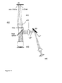
- FIG. 1 represents a schematic view of a fluorescence PAM 100 according to the invention.
- the PAM 100 basically includes a light source 110 which is a white lamp or a laser source, a DMD 120 operating as a SLM, imaging optics 130, a probe portion 140 and a detection system 150, 160.
- the DMD 120 consists of an array of square mirrors 121a, 121b,... (only one element is illustrated, resp.) each of which can be separately tilted into two stable resting states over a predetermined tilt angle ⁇ ⁇ to the normal.
- the value of the tilt angle ⁇ depends on the DMD practically used.
- Each mirror element can be switched between the resting states with characteristic frequencies in the kHz-range according to a predetermined modulation pattern.
- the resting states are called "on"- and “off”-positions according to which the respective conjugate contributions and the non-conjugate contributions of the detected light (fluorescence or reflection) are deflected to the detection system 150, 160. Both contributions yield a focal conjugate image I c and a non-conjugate image I nc , resp., on the basis of which the desired confocal image is obtained as outlined below.
- the detection system 150, 160 is a common path dual reflection system. This nomenclature is used for the following reason.
- the "common path” refers to the fact that illumination and detection follow an essentially common optical path between the illumination and detection apertures.
- the “dual reflection” refers to the fact that the SLM elements can direct light along two subsequent optical paths. Accordingly, the images I nc and I c (see below) can be collected simultaneously.
- An alternative is described below as a dual path single reflection system ( Figure 4).
- each path contains a two-dimensional camera 151, 161 and detection optics 111, 112, 162, resp..
- the camera 151 is adapted to detect the light reflected by the mirrors in the "on"-position while the camera 161 receives light reflected in the "off"-position.
- the modulation pattern of the SLM (DMD 120) is changed N times in order to generate a confocal image (scanning).
- the i-th modulation of the SLM is denoted with: where x d ,y d are continuous coordinates of the SLM and the shape and finite size of the elements (mirrors) is included in S i .
- the modulations S i are preferably selected according to a grid pattern approach or a pseudorandom sequence approach which are described in the following.
- the grid pattern approach has the advantage of easy implementation and yielding a confocal image without post-processing. Although some post-processing is needed in the pseudorandom sequence approach, the frame integration time for a given signal level can be essentially shorter.
- the real lattice parameters being contained in the function G can yield different suitable shapes. These shapes comprise e.g. square shapes, but pseudo-hexagonal grids or line patterns or more complex shapes are also possible.
- the focal conjugate image of an object O(x 0 ,y 0 ,z 0 ) in a coordinate system (x 0 ,y 0 ,z 0 ) in an object space, with a scanning in the axial direction by displacement over the distance z s is given by: wherein M is the magnification, T the total frame integration time and H em (x 0 ,y 0 ,z 0 ) the emission PSF (point spread function) of the objective.
- I G is the total illumination according to: wherein H ex (x 0 ,y 0 ,z 0 ) the excitation PSF of the objective.
- the image according to eq. (4) can be viewed as a three-dimensional convolution with a spatially varying PSF, due to the dependence of ⁇ x , ⁇ y , x d and y d .
- the SLM cannot scan continuously and G(x d ,y d ) can (contrary to the continuous motion in known microscopes as e.g. in so-called tandem scanning microscopes) only shift over integer multiples of ⁇ .
- the distinction is negligible if ⁇ /M is small compared to the sampling density of the image. For very large ⁇ , a pixelation of the image can occur.
- the PSF can be made spatially invariant by scanning the SLM over ⁇ (so-called dithering).
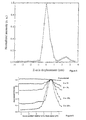
- the results are normalized compared with the image of a conventional microscope and an ideal confocal microscope.
- the conventional response deviates from the expected straight line as a result of simulating an infinitely large object in a finite sized image.
- the pseudorandom sequence approach is very light efficient as 50% of all SLM elements are "on". This is supported by eq. (9) which equals to eq. (4) except of coefficient T/4 instead of T/n x n y in the second term. Although both approaches yield the same confocal image for the same grid G (x d ,y d ), the pseudorandom sequence generates a much larger signal, whose strength is independent of the sequence length.
- the enhancement algorithm can be a nearest-neighbor approach where three or more sections are used to generate one single enhanced image or an algorithm where 3D-stacks of images are used for a full 3D reconstruction as it is described by P. J. Verveer and T. M. Jovin in "Journal of the Optical Society of America A” (vol. 14, 1997, p. 1696-1706). The latter model is cited in the following in matrix notation.
- the dimensionality of the image is irrelevant.
- the implementation of H depends on the dimensionality, but the algorithms themselves do not. Normally, the dimensionality is equal to 3 (spatial dimensions). However, further dimensions such as spectral or time dimensions can be added with only a change of H . For instance, if a time dependency is measured for each image pixel or for groups of image pixels, the dimensionality is equal to 4. If blurring is present in the time dimension, it can be deconvoluted from the data by extending H with the time dimension.
- the capability to apply these deconvolution algorithms also in the spectral and time dimensions, whereas previously they have been restricted to the spatial dimensions, represents an essential advantage of the invention.
- FIG 3 shows a schematic view of a common path dual reflection PAM 300 according to the invention.
- PAM 300 basically includes a light source 310, a SLM 320, imaging optics 330, a probe portion 340 and detection systems 350, 360.
- PAM 300 can be implemented with a Digital Light Processing kit (e. g. of Texas Instruments, Dallas, USA) as a light source in combination with a microscope with side illumination ports (e. g. Zeiss Axioplan) and CCD cameras (e. g. CH220 cameras of Photometrics, Arlington, USA, with Kodak KAF1400 CCD sensors).
- a Digital Light Processing kit e. g. of Texas Instruments, Dallas, USA
- side illumination ports e. g. Zeiss Axioplan
- CCD cameras e. g. CH220 cameras of Photometrics, Arlington, USA, with Kodak KAF1400 CCD sensors.
- the focal conjugate image I c is collected with camera 351 and the non-conjugate image I nc is collected with camera 361.
- Figure 4 shows a schematic view of a dual path single reflection PAM 400 being another embodiment of the invention.
- the "dual path" refers to the fact that illumination and detection follow two different optical paths.
- the SLM is capable of directing light in two directions, only a single reflection direction is used. While in the embodiment of Figure 3, the confocality is defined by the same SLM element, according to Figure 4 the confocality is definded by the SLM element on the illuminations side and by the CCD pixels on the detection side.
- PAM 400 is adapted in a simplified manner to a conventional microscope with one optical axis on which the probe portion 440, imaging optics 430 and the detection system 450 are arranged.
- the microscope can comprise the same basic components as noted above.
- the illumination light from the light source 410 is reflected via the SLM 420 and a side port of the microscope to a beam splitter (e. g. half-silvered mirror) in the optical axis.
- FIG. 6 An experimental verification of the supression of background signal during optical sectioning is shown in Figure 6.
- a reflective surface (mirror) is scanned along the z-axis through the focus plane.
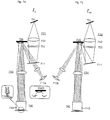
- Figures 7A and 7B show an alternative example of common path dual reflection PAM 700 with two illumination axes using only a single camera for image collection. This concept has certain advantages as to the cost saving use of only one camera and the simpler optical alignment of the elements forming the optical paths for the images I c and I nc .
- PAM 700 comprises basically similiar components as PAM 300 shown in Figure 3, in particular light sources 710a, 710b, a SLM 720, imaging optics 730, an objective 743, a probe portion 740 and a detection system 750.
- the collection of one full image is accomplished in two steps. For the collection of image sequences, the images I c and I nc are collected alternately.
- First the image I c is collected by illuminating the object from a first side with the light source 710a via a semitransmissive mirror 711, the SLM 720 and the imaging optics 730 and detecting the focal plane image along the reversed optical path via the SLM 720, the semitransmissive mirror 711, a filter 753, a lens 752 with the camera 751.
- This situation is shown in Figure 7A.
- the pattern used for controlling the SLM 720 is called the "positive" representation corresponding to the pseudo-random or other sequences displayed on the SLM.
- the two-sided illumination can be implemented according to various ways, e. g. by a single light source being directed by mirrors along the two illumination axes or by two identical light sources.
Landscapes
- Physics & Mathematics (AREA)
- General Physics & Mathematics (AREA)
- Optics & Photonics (AREA)
- Chemical & Material Sciences (AREA)
- Analytical Chemistry (AREA)
- Engineering & Computer Science (AREA)
- Computer Vision & Pattern Recognition (AREA)
- General Engineering & Computer Science (AREA)
- Microscoopes, Condenser (AREA)
- Liquid Crystal (AREA)
- Investigating, Analyzing Materials By Fluorescence Or Luminescence (AREA)
Priority Applications (5)
| Application Number | Priority Date | Filing Date | Title |
|---|---|---|---|
| AT97118354T ATE236412T1 (de) | 1997-10-22 | 1997-10-22 | Programmierbares räumlich lichtmoduliertes mikroskop und mikroskopieverfahren |
| EP97118354A EP0911667B1 (en) | 1997-10-22 | 1997-10-22 | Programmable spatially light modulated microscope and microscopy method |
| DE69720458T DE69720458T2 (de) | 1997-10-22 | 1997-10-22 | Programmierbares räumlich lichtmoduliertes Mikroskop und Mikroskopieverfahren |
| US09/176,240 US6399935B1 (en) | 1997-10-22 | 1998-10-21 | Programmable spatially light modulated microscope ND microscopy |
| JP30100398A JP4064550B2 (ja) | 1997-10-22 | 1998-10-22 | プログラム可能であり空間的に光変調された顕微鏡および顕微鏡による方法 |
Applications Claiming Priority (1)
| Application Number | Priority Date | Filing Date | Title |
|---|---|---|---|
| EP97118354A EP0911667B1 (en) | 1997-10-22 | 1997-10-22 | Programmable spatially light modulated microscope and microscopy method |
Publications (2)
| Publication Number | Publication Date |
|---|---|
| EP0911667A1 EP0911667A1 (en) | 1999-04-28 |
| EP0911667B1 true EP0911667B1 (en) | 2003-04-02 |
Family
ID=8227511
Family Applications (1)
| Application Number | Title | Priority Date | Filing Date |
|---|---|---|---|
| EP97118354A Expired - Lifetime EP0911667B1 (en) | 1997-10-22 | 1997-10-22 | Programmable spatially light modulated microscope and microscopy method |
Country Status (5)
Cited By (4)
| Publication number | Priority date | Publication date | Assignee | Title |
|---|---|---|---|---|
| DE102005058185A1 (de) * | 2005-12-01 | 2007-06-14 | Friedrich-Schiller-Universität Jena | Verfahren und Anordnung zur Detektion von Fluoreszenz- oder Reflexionsspektren beliebig wählbarer Bereiche und Strukturen eines vom Fremdlicht überlagerten Objekts unter geringer Strahlenbelastung |
| EP2369401A1 (en) * | 2010-03-23 | 2011-09-28 | Max-Planck-Gesellschaft zur Förderung der Wissenschaften e.V. | Optical modulator device and spatio-temporally light modulated imaging system |
| CN101655601B (zh) * | 2008-08-22 | 2012-09-26 | 麦克奥迪实业集团有限公司 | 一种基于dmd的结构光显微镜成像方法及系统 |
| DE102012217329A1 (de) * | 2012-09-25 | 2014-06-12 | Carl Zeiss Ag | Projektionsvorrichtung |
Families Citing this family (96)
| Publication number | Priority date | Publication date | Assignee | Title |
|---|---|---|---|---|
| CA2307315C (en) | 1997-10-29 | 2011-04-05 | Calum Eric Macaulay | Apparatus and methods relating to spatially light modulated microscopy |
| US6388809B1 (en) | 1997-10-29 | 2002-05-14 | Digital Optical Imaging Corporation | Methods and apparatus for improved depth resolution use of out-of-focus information in microscopy |
| GB9901365D0 (en) * | 1999-01-22 | 1999-03-10 | Isis Innovations Ltd | Confocal microscopy apparatus and method |
| JP3544892B2 (ja) * | 1999-05-12 | 2004-07-21 | 株式会社東京精密 | 外観検査方法及び装置 |
| US6700606B1 (en) * | 1999-06-09 | 2004-03-02 | Activcard Ireland Limited | Micromirror optical imager |
| DE19932487A1 (de) * | 1999-07-09 | 2001-02-08 | Epigenomics Gmbh | Vorrichtung und Verfahren zur photolithographischen Belichtung von biologischen Stoffen |
| DE19960583A1 (de) * | 1999-12-15 | 2001-07-05 | Evotec Biosystems Ag | Verfahren und Vorrichtung zur Mikroskopie |
| US6663560B2 (en) * | 1999-12-17 | 2003-12-16 | Digital Optical Imaging Corporation | Methods and apparatus for imaging using a light guide bundle and a spatial light modulator |
| US6530882B1 (en) * | 2000-06-30 | 2003-03-11 | Inner Vision Imaging, L.L.C. | Endoscope having microscopic and macroscopic magnification |
| JP4610713B2 (ja) * | 2000-10-13 | 2011-01-12 | オリンパス株式会社 | 内視鏡装置 |
| JP4932076B2 (ja) * | 2000-10-30 | 2012-05-16 | オリンパス株式会社 | 走査型レーザ顕微鏡 |
| JP4153675B2 (ja) * | 2001-04-10 | 2008-09-24 | 三菱重工業株式会社 | 材料寿命の評価システム、及び、その評価方法 |
| CA2452693A1 (en) * | 2001-06-06 | 2002-12-12 | Digital Optical Imaging Corporation | Light modulated microarray reader and methods relating thereto |
| WO2003025656A1 (fr) * | 2001-09-03 | 2003-03-27 | Kabushiki Kaisha Hayashi Soken | Procede et dispositif de balayage a commande numerique |
| US6885492B2 (en) * | 2001-11-08 | 2005-04-26 | Imaginative Optics, Inc. | Spatial light modulator apparatus |
| US7180660B2 (en) * | 2002-02-04 | 2007-02-20 | Carl-Zeiss-Stiftung Trading As Carl Zeiss | Stereo-examination systems and stereo-image generation apparatus as well as a method for operating the same |
| US6996292B1 (en) * | 2002-04-18 | 2006-02-07 | Sandia Corporation | Staring 2-D hadamard transform spectral imager |
| US7193775B2 (en) * | 2002-05-30 | 2007-03-20 | Dmetrix, Inc. | EPI-illumination system for an array microscope |
| JP3691837B2 (ja) * | 2002-08-16 | 2005-09-07 | 株式会社林創研 | バイオチップ分析装置 |
| US7901630B2 (en) | 2002-08-20 | 2011-03-08 | Illumina, Inc. | Diffraction grating-based encoded microparticle assay stick |
| US7872804B2 (en) | 2002-08-20 | 2011-01-18 | Illumina, Inc. | Encoded particle having a grating with variations in the refractive index |
| US7923260B2 (en) | 2002-08-20 | 2011-04-12 | Illumina, Inc. | Method of reading encoded particles |
| US7900836B2 (en) | 2002-08-20 | 2011-03-08 | Illumina, Inc. | Optical reader system for substrates having an optically readable code |
| US7164533B2 (en) | 2003-01-22 | 2007-01-16 | Cyvera Corporation | Hybrid random bead/chip based microarray |
| US7508608B2 (en) | 2004-11-17 | 2009-03-24 | Illumina, Inc. | Lithographically fabricated holographic optical identification element |
| US7092160B2 (en) | 2002-09-12 | 2006-08-15 | Illumina, Inc. | Method of manufacturing of diffraction grating-based optical identification element |
| US20100255603A9 (en) | 2002-09-12 | 2010-10-07 | Putnam Martin A | Method and apparatus for aligning microbeads in order to interrogate the same |
| WO2004038461A2 (en) * | 2002-10-22 | 2004-05-06 | William Marsh Rice University | Random access high-speed confocal microscope |
| FR2848682B1 (fr) | 2002-12-13 | 2005-02-18 | Commissariat Energie Atomique | Microscope optique a eclairage structure modifiable |
| US7339148B2 (en) * | 2002-12-16 | 2008-03-04 | Olympus America Inc. | Confocal microscope |
| US7002164B2 (en) * | 2003-01-08 | 2006-02-21 | Intel Corporation | Source multiplexing in lithography |
| US8081792B2 (en) | 2003-08-20 | 2011-12-20 | Illumina, Inc. | Fourier scattering methods for encoding microbeads and methods and apparatus for reading the same |
| JP4031716B2 (ja) * | 2003-02-06 | 2008-01-09 | 株式会社コーナン・メディカル | 眼科用撮影装置 |
| DE10327987A1 (de) * | 2003-06-21 | 2005-01-20 | MAX-PLANCK-Gesellschaft zur Förderung der Wissenschaften e.V. | Konfokales optisches System |
| US7881502B2 (en) * | 2003-06-30 | 2011-02-01 | Weyerhaeuser Nr Company | Method and system for three-dimensionally imaging an apical dome of a plant embryo |
| EP1972983B1 (fr) * | 2003-07-04 | 2009-12-02 | Vincent Lauer | Dispositif d`imagerie à balayage pour microscopie confocale à soustraction d`images |
| US8269174B2 (en) * | 2003-07-18 | 2012-09-18 | Chemimage Corporation | Method and apparatus for compact spectrometer for multipoint sampling of an object |
| US7433123B2 (en) | 2004-02-19 | 2008-10-07 | Illumina, Inc. | Optical identification element having non-waveguide photosensitive substrate with diffraction grating therein |
| WO2006020363A2 (en) | 2004-07-21 | 2006-02-23 | Illumina, Inc. | Method and apparatus for drug product tracking using encoded optical identification elements |
| EP1622200A1 (en) | 2004-07-26 | 2006-02-01 | CSEM Centre Suisse d'Electronique et de Microtechnique SA | Solid-state photodetector pixel and photodetecting method |
| US20060066842A1 (en) * | 2004-09-30 | 2006-03-30 | Saunders Winston A | Wafer inspection with a customized reflective optical channel component |
| JP2006133499A (ja) * | 2004-11-05 | 2006-05-25 | Shimadzu Corp | 共焦点スキャナ及び共焦点顕微鏡 |
| US7602952B2 (en) * | 2004-11-16 | 2009-10-13 | Illumina, Inc. | Scanner having spatial light modulator |
| JP2006154290A (ja) * | 2004-11-29 | 2006-06-15 | Hamamatsu Univ School Of Medicine | 蛍光顕微鏡システム |
| JP2006235420A (ja) * | 2005-02-28 | 2006-09-07 | Yokogawa Electric Corp | 共焦点顕微鏡 |
| JP3755888B2 (ja) * | 2005-06-14 | 2006-03-15 | 株式会社林創研 | バイオチップオンライン分析システム |
| GB0514656D0 (en) | 2005-07-16 | 2005-08-24 | Cairn Res Ltd | Control of illumination in microscopy |
| EP1746410B1 (en) | 2005-07-21 | 2018-08-22 | CSEM Centre Suisse d'Electronique et de Microtechnique SA - Recherche et Développement | Apparatus and method for fluorescence lifetime imaging |
| DE102005040471B4 (de) * | 2005-08-26 | 2007-06-21 | Leica Microsystems (Schweiz) Ag | Mikroskop |
| US7593156B2 (en) * | 2005-08-26 | 2009-09-22 | Leica Microsystems (Schweiz) Ag | Microscope with micro-mirrors for optional deflection and/or beam splitting |
| DE502005010557D1 (de) * | 2005-09-13 | 2010-12-30 | Univ Albert Ludwigs Freiburg | Mikroskopieverfahren mit räumlich modulierbarer Beleuchtung |
| EP1936422A4 (en) * | 2005-10-13 | 2013-01-16 | Nikon Corp | MICROSCOPE |
| JP2007171598A (ja) * | 2005-12-22 | 2007-07-05 | Olympus Corp | 共焦点顕微鏡 |
| GB0606788D0 (en) * | 2006-04-03 | 2006-05-10 | Ind Co Ltd | Confocal microscopy |
| US7830575B2 (en) | 2006-04-10 | 2010-11-09 | Illumina, Inc. | Optical scanner with improved scan time |
| US8254020B2 (en) * | 2006-04-20 | 2012-08-28 | Washington University | Objective-coupled selective plane illumination microscopy |
| DE102006040636B3 (de) * | 2006-05-15 | 2007-12-20 | Leica Microsystems (Schweiz) Ag | Autofokus-System und Verfahren zum Autofokussieren |
| US7460248B2 (en) * | 2006-05-15 | 2008-12-02 | Carestream Health, Inc. | Tissue imaging system |
| DE102006022592B4 (de) * | 2006-05-15 | 2008-02-07 | Leica Microsystems (Schweiz) Ag | Mikroskop mit Beleuchtungseinheit |
| DE102006025149A1 (de) * | 2006-05-30 | 2007-12-06 | Leica Microsystems (Schweiz) Ag | Optisches Gerät mit erhöhter Tiefenschärfe |
| DE102006027836B4 (de) * | 2006-06-16 | 2020-02-20 | Carl Zeiss Microscopy Gmbh | Mikroskop mit Autofokuseinrichtung |
| US7990524B2 (en) * | 2006-06-30 | 2011-08-02 | The University Of Chicago | Stochastic scanning apparatus using multiphoton multifocal source |
| JP4891057B2 (ja) * | 2006-12-27 | 2012-03-07 | オリンパス株式会社 | 共焦点レーザー走査型顕微鏡 |
| DE102008011993A1 (de) | 2008-02-29 | 2009-09-10 | Leica Microsystems Cms Gmbh | Synchronisierte Bildgebung mittels optischer Verfahren und Rasterkraftmikroskopie |
| US8531662B2 (en) * | 2008-06-17 | 2013-09-10 | Koninklijke Philips N.V. | Method and device for optically examining the interior of turbid media |
| US9846313B2 (en) | 2008-09-25 | 2017-12-19 | The Trustees Of Columbia University In The City Of New York | Devices, apparatus and method for providing photostimulation and imaging of structures |
| KR101495096B1 (ko) * | 2008-10-31 | 2015-02-25 | 삼성전자주식회사 | 협대역 엑스레이 필터링 장치 및 방법 |
| EP3667391A1 (de) * | 2009-10-28 | 2020-06-17 | Carl Zeiss Microscopy GmbH | Mikroskopisches verfahren und mikroskop mit gesteigerter auflösung |
| JP5393406B2 (ja) * | 2009-11-06 | 2014-01-22 | オリンパス株式会社 | パターン投影装置、走査型共焦点顕微鏡、及びパターン照射方法 |
| EP2501288B1 (en) * | 2009-11-19 | 2016-12-21 | Modulated Imaging Inc. | Method and apparatus for analysis of turbid media via single-element detection using structured illumination |
| DE102009047198A1 (de) * | 2009-11-26 | 2011-06-01 | Universität Rostock | Mikroarraybasiertes Ortsfilter |
| US8237835B1 (en) * | 2011-05-19 | 2012-08-07 | Aeon Imaging, LLC | Confocal imaging device using spatially modulated illumination with electronic rolling shutter detection |
| DE102012009836A1 (de) | 2012-05-16 | 2013-11-21 | Carl Zeiss Microscopy Gmbh | Lichtmikroskop und Verfahren zur Bildaufnahme mit einem Lichtmikroskop |
| CN102928970B (zh) * | 2012-10-19 | 2014-10-29 | 华中科技大学 | 一种大样本快速三维显微成像的方法和系统 |
| DE102013001238B4 (de) * | 2013-01-25 | 2020-06-10 | Carl Zeiss Microscopy Gmbh | Lichtmikroskop und Mikroskopieverfahren |
| CN103364345B (zh) * | 2013-06-25 | 2015-11-11 | 浙江大学 | 基于数字微镜元件的全反射显微镜环形扫描方法和装置 |
| US9535242B1 (en) * | 2014-06-26 | 2017-01-03 | Verily Life Sciences Llc | Parallel programmable array microscope |
| US9485491B2 (en) * | 2014-12-15 | 2016-11-01 | Test Research, Inc. | Optical system |
| KR20160115682A (ko) * | 2015-03-25 | 2016-10-06 | 삼성전자주식회사 | 대상에 대하여 공간적으로 가변하는 오토 포커싱을 가능하게 하는 방법 및 이를 이용하는 촬상 시스템 |
| DE102015210016A1 (de) * | 2015-06-01 | 2016-12-01 | Carl Zeiss Microscopy Gmbh | Verfahren zum Ermitteln einer ortsaufgelösten Höheninformation einer Probe mit einem Weitfeldmikroskop und Weitfeldmikroskop |
| CN105092603B (zh) * | 2015-09-07 | 2017-09-05 | 哈尔滨理工大学 | 碗型工件内壁的在线视觉检测装置和方法 |
| US10386300B2 (en) | 2015-12-21 | 2019-08-20 | Verily Life Sciences Llc | Spectrally and spatially multiplexed fluorescent probes for in situ cell labeling |
| EP3433657A1 (en) | 2016-03-24 | 2019-01-30 | Max-Planck-Gesellschaft zur Förderung der Wissenschaften e.V. | Spatio-temporally light modulated imaging system including vertical cameras, and method for confocal imaging an object |
| JP6815412B2 (ja) * | 2016-03-24 | 2021-01-20 | マツクス−プランク−ゲゼルシヤフト ツール フエルデルング デル ヴイツセンシヤフテン エー フアウMAX−PLANCK−GESELLSCHAFT ZUR FOeRDERUNG DER WISSENSCHAFTEN E.V. | 時空間光変調結像システム、物体を共焦点結像させる方法、およびキャリア・ホイール装置 |
| JP6795624B2 (ja) | 2016-05-27 | 2020-12-02 | ヴェリリー ライフ サイエンシズ エルエルシー | 空間光変調器ベースのハイパースペクトル共焦点顕微鏡および使用方法 |
| DE102016119727A1 (de) * | 2016-10-17 | 2018-04-19 | Carl Zeiss Microscopy Gmbh | Vorrichtung zur Strahlmanipulation für ein Scanning-Mikroskop und Mikroskop |
| KR101907782B1 (ko) | 2017-04-12 | 2018-10-12 | 한국과학기술원 | 광학 현미경 장치 및 시편의 영상 측정 방법 |
| JP2019066706A (ja) | 2017-10-02 | 2019-04-25 | ソニー株式会社 | 蛍光顕微鏡装置及び蛍光顕微鏡システム |
| US20210003834A1 (en) * | 2017-12-20 | 2021-01-07 | Max-Planck-Gesellschaft Zur Foerderung Der Wissenschaften E. V. | Method and apparatus for optical confocal imaging, using a programmable array microscope |
| JP7260966B2 (ja) * | 2018-02-19 | 2023-04-19 | 京セラ株式会社 | 電磁波検出装置 |
| WO2019159933A1 (ja) * | 2018-02-19 | 2019-08-22 | 京セラ株式会社 | 電磁波検出装置および情報取得システム |
| JP7380569B2 (ja) | 2018-08-09 | 2023-11-15 | ソニーグループ株式会社 | 光学顕微鏡装置及び光学顕微鏡システム |
| DE102018127281A1 (de) * | 2018-10-31 | 2020-04-30 | Carl Zeiss Microscopy Gmbh | Mikroskop und Verfahren zur Mikroskopie |
| DE102019110869A1 (de) * | 2018-12-21 | 2020-06-25 | Leica Microsystems Cms Gmbh | Mikroskop |
| CN113302520B (zh) * | 2019-01-16 | 2024-07-02 | 株式会社小糸制作所 | 成像装置、其运算处理装置、车辆用灯具、车辆、感测方法 |
| EP4052084B1 (en) * | 2020-01-13 | 2023-10-11 | Haag-Streit Ag | Ophthalmologic microscope with micro-mirror balancing |
Family Cites Families (6)
| Publication number | Priority date | Publication date | Assignee | Title |
|---|---|---|---|---|
| EP0485803B1 (de) * | 1990-11-10 | 1996-05-01 | Grosskopf, Rudolf, Dr.-Ing. | Optische Abtastvorrichtung mit konfokalem Strahlengang, in der Lichtquellen- und Detektormatrix verwendet werden |
| US5532873A (en) * | 1993-09-08 | 1996-07-02 | Dixon; Arthur E. | Scanning beam laser microscope with wide range of magnification |
| US5587832A (en) * | 1993-10-20 | 1996-12-24 | Biophysica Technologies, Inc. | Spatially light modulated confocal microscope and method |
| GB9603788D0 (en) * | 1996-02-22 | 1996-04-24 | Isis Innovation | Confocal microscope |
| JP2001500628A (ja) * | 1996-02-28 | 2001-01-16 | ケニス シー ジョンソン | マイクロリトグラフィ用マイクロレンズスキャナ及び広フィールド共焦顕微鏡 |
| US6038067A (en) * | 1996-05-23 | 2000-03-14 | The Regents Of The University Of California | Scanning computed confocal imager |
-
1997
- 1997-10-22 DE DE69720458T patent/DE69720458T2/de not_active Expired - Lifetime
- 1997-10-22 EP EP97118354A patent/EP0911667B1/en not_active Expired - Lifetime
- 1997-10-22 AT AT97118354T patent/ATE236412T1/de not_active IP Right Cessation
-
1998
- 1998-10-21 US US09/176,240 patent/US6399935B1/en not_active Expired - Lifetime
- 1998-10-22 JP JP30100398A patent/JP4064550B2/ja not_active Expired - Lifetime
Cited By (6)
| Publication number | Priority date | Publication date | Assignee | Title |
|---|---|---|---|---|
| DE102005058185A1 (de) * | 2005-12-01 | 2007-06-14 | Friedrich-Schiller-Universität Jena | Verfahren und Anordnung zur Detektion von Fluoreszenz- oder Reflexionsspektren beliebig wählbarer Bereiche und Strukturen eines vom Fremdlicht überlagerten Objekts unter geringer Strahlenbelastung |
| CN101655601B (zh) * | 2008-08-22 | 2012-09-26 | 麦克奥迪实业集团有限公司 | 一种基于dmd的结构光显微镜成像方法及系统 |
| EP2369401A1 (en) * | 2010-03-23 | 2011-09-28 | Max-Planck-Gesellschaft zur Förderung der Wissenschaften e.V. | Optical modulator device and spatio-temporally light modulated imaging system |
| US9279971B2 (en) | 2010-03-23 | 2016-03-08 | Max-Planck-Gesellschaft Zur Foerderung Der Wissenschaften E.V. | Optical modulator device and spatio-temporally light modulated imaging system |
| DE102012217329A1 (de) * | 2012-09-25 | 2014-06-12 | Carl Zeiss Ag | Projektionsvorrichtung |
| DE102012217329B4 (de) | 2012-09-25 | 2024-03-21 | Carl Zeiss Jena Gmbh | Projektionsvorrichtung |
Also Published As
| Publication number | Publication date |
|---|---|
| DE69720458T2 (de) | 2004-02-26 |
| EP0911667A1 (en) | 1999-04-28 |
| DE69720458D1 (de) | 2003-05-08 |
| JPH11194275A (ja) | 1999-07-21 |
| US6399935B1 (en) | 2002-06-04 |
| ATE236412T1 (de) | 2003-04-15 |
| JP4064550B2 (ja) | 2008-03-19 |
Similar Documents
| Publication | Publication Date | Title |
|---|---|---|
| EP0911667B1 (en) | Programmable spatially light modulated microscope and microscopy method | |
| Verveer et al. | Theory of confocal fluorescence imaging in the programmable array microscope (PAM) | |
| US10591417B2 (en) | Systems and methods for 4-D hyperspectral imaging | |
| CN110262026B (zh) | 孔径扫描傅立叶重叠关联成像 | |
| EP0916981B1 (en) | Confocal spectroscopy system and method | |
| US8705172B2 (en) | Microscopy method and microscope with enhanced resolution | |
| US9086536B2 (en) | Talbot imaging devices and systems | |
| US5923466A (en) | Light modulated confocal optical instruments and method | |
| Inoué | Foundations of confocal scanned imaging in light microscopy | |
| CN112930492B (zh) | 用于使用时间复用光片的快速体积荧光显微术的装置和方法 | |
| US20090218527A1 (en) | Confocal Microscopy with a Two-Dimensional Array of Light Emitting Diodes | |
| CA2921372A1 (en) | Variable-illumination fourier ptychographic imaging devices, systems, and methods | |
| Hanley et al. | Optical sectioning fluorescence spectroscopy in a programmable array microscope | |
| CA3065917A1 (en) | Super-resolution line scanning confocal microscopy with pupil filtering | |
| US20240255428A1 (en) | Enhanced resolution imaging | |
| WO2013176549A1 (en) | Optical apparatus for multiple points of view three-dimensional microscopy and method | |
| US20200049968A1 (en) | Flexible light sheet generation by field synthesis | |
| Vitali | Selective volume illumination microscopy for compressed sensing of time lapse series | |
| EP3901684A1 (en) | Optical fluorescence microscope and method for the obtaining of optical fluorescence microscopy images | |
| Lahrberg | Novel strategies for super-resolution fluorescence microscopy | |
| Hirata Miyasaki | Deep and Fast High-Resolution 3D Microscopy | |
| Landry | High-Speed Isotropic Resolution and Structured Illumination Using Phased Arrays In Light Sheet Fluorescence Microscopy | |
| CN117929335A (zh) | 成像装置、成像方法、电子设备及计算机可读存储介质 | |
| Carrington et al. | High resolution 3-D imaging of living cells by image restoration | |
| Hanley et al. | Programmable Array Microscopes |
Legal Events
| Date | Code | Title | Description |
|---|---|---|---|
| PUAI | Public reference made under article 153(3) epc to a published international application that has entered the european phase |
Free format text: ORIGINAL CODE: 0009012 |
|
| AK | Designated contracting states |
Kind code of ref document: A1 Designated state(s): AT BE CH DE DK ES FI FR GB GR IE IT LI LU MC NL PT SE |
|
| AX | Request for extension of the european patent |
Free format text: AL;LT;LV;RO;SI |
|
| 17P | Request for examination filed |
Effective date: 19990916 |
|
| AKX | Designation fees paid |
Free format text: AT BE CH DE DK ES FI FR GB GR IE IT LI LU MC NL PT SE |
|
| GRAH | Despatch of communication of intention to grant a patent |
Free format text: ORIGINAL CODE: EPIDOS IGRA |
|
| GRAH | Despatch of communication of intention to grant a patent |
Free format text: ORIGINAL CODE: EPIDOS IGRA |
|
| GRAA | (expected) grant |
Free format text: ORIGINAL CODE: 0009210 |
|
| AK | Designated contracting states |
Designated state(s): AT BE CH DE DK ES FI FR GB GR IE IT LI LU MC NL PT SE |
|
| PG25 | Lapsed in a contracting state [announced via postgrant information from national office to epo] |
Ref country code: NL Free format text: LAPSE BECAUSE OF FAILURE TO SUBMIT A TRANSLATION OF THE DESCRIPTION OR TO PAY THE FEE WITHIN THE PRESCRIBED TIME-LIMIT Effective date: 20030402 Ref country code: LI Free format text: LAPSE BECAUSE OF FAILURE TO SUBMIT A TRANSLATION OF THE DESCRIPTION OR TO PAY THE FEE WITHIN THE PRESCRIBED TIME-LIMIT Effective date: 20030402 Ref country code: IT Free format text: LAPSE BECAUSE OF FAILURE TO SUBMIT A TRANSLATION OF THE DESCRIPTION OR TO PAY THE FEE WITHIN THE PRESCRIBED TIME-LIMIT;WARNING: LAPSES OF ITALIAN PATENTS WITH EFFECTIVE DATE BEFORE 2007 MAY HAVE OCCURRED AT ANY TIME BEFORE 2007. THE CORRECT EFFECTIVE DATE MAY BE DIFFERENT FROM THE ONE RECORDED. Effective date: 20030402 Ref country code: FR Free format text: LAPSE BECAUSE OF FAILURE TO SUBMIT A TRANSLATION OF THE DESCRIPTION OR TO PAY THE FEE WITHIN THE PRESCRIBED TIME-LIMIT Effective date: 20030402 Ref country code: FI Free format text: LAPSE BECAUSE OF FAILURE TO SUBMIT A TRANSLATION OF THE DESCRIPTION OR TO PAY THE FEE WITHIN THE PRESCRIBED TIME-LIMIT Effective date: 20030402 Ref country code: CH Free format text: LAPSE BECAUSE OF FAILURE TO SUBMIT A TRANSLATION OF THE DESCRIPTION OR TO PAY THE FEE WITHIN THE PRESCRIBED TIME-LIMIT Effective date: 20030402 Ref country code: BE Free format text: LAPSE BECAUSE OF FAILURE TO SUBMIT A TRANSLATION OF THE DESCRIPTION OR TO PAY THE FEE WITHIN THE PRESCRIBED TIME-LIMIT Effective date: 20030402 Ref country code: AT Free format text: LAPSE BECAUSE OF FAILURE TO SUBMIT A TRANSLATION OF THE DESCRIPTION OR TO PAY THE FEE WITHIN THE PRESCRIBED TIME-LIMIT Effective date: 20030402 |
|
| REG | Reference to a national code |
Ref country code: GB Ref legal event code: FG4D |
|
| REG | Reference to a national code |
Ref country code: CH Ref legal event code: EP |
|
| REG | Reference to a national code |
Ref country code: IE Ref legal event code: FG4D |
|
| REF | Corresponds to: |
Ref document number: 69720458 Country of ref document: DE Date of ref document: 20030508 Kind code of ref document: P |
|
| PG25 | Lapsed in a contracting state [announced via postgrant information from national office to epo] |
Ref country code: SE Free format text: LAPSE BECAUSE OF FAILURE TO SUBMIT A TRANSLATION OF THE DESCRIPTION OR TO PAY THE FEE WITHIN THE PRESCRIBED TIME-LIMIT Effective date: 20030702 Ref country code: PT Free format text: LAPSE BECAUSE OF FAILURE TO SUBMIT A TRANSLATION OF THE DESCRIPTION OR TO PAY THE FEE WITHIN THE PRESCRIBED TIME-LIMIT Effective date: 20030702 Ref country code: GR Free format text: LAPSE BECAUSE OF FAILURE TO SUBMIT A TRANSLATION OF THE DESCRIPTION OR TO PAY THE FEE WITHIN THE PRESCRIBED TIME-LIMIT Effective date: 20030702 Ref country code: DK Free format text: LAPSE BECAUSE OF FAILURE TO SUBMIT A TRANSLATION OF THE DESCRIPTION OR TO PAY THE FEE WITHIN THE PRESCRIBED TIME-LIMIT Effective date: 20030702 |
|
| NLV1 | Nl: lapsed or annulled due to failure to fulfill the requirements of art. 29p and 29m of the patents act | ||
| REG | Reference to a national code |
Ref country code: CH Ref legal event code: PL |
|
| PG25 | Lapsed in a contracting state [announced via postgrant information from national office to epo] |
Ref country code: LU Free format text: LAPSE BECAUSE OF NON-PAYMENT OF DUE FEES Effective date: 20031022 Ref country code: IE Free format text: LAPSE BECAUSE OF NON-PAYMENT OF DUE FEES Effective date: 20031022 |
|
| PG25 | Lapsed in a contracting state [announced via postgrant information from national office to epo] |
Ref country code: ES Free format text: LAPSE BECAUSE OF FAILURE TO SUBMIT A TRANSLATION OF THE DESCRIPTION OR TO PAY THE FEE WITHIN THE PRESCRIBED TIME-LIMIT Effective date: 20031030 |
|
| PG25 | Lapsed in a contracting state [announced via postgrant information from national office to epo] |
Ref country code: MC Free format text: LAPSE BECAUSE OF NON-PAYMENT OF DUE FEES Effective date: 20031031 |
|
| PLBE | No opposition filed within time limit |
Free format text: ORIGINAL CODE: 0009261 |
|
| STAA | Information on the status of an ep patent application or granted ep patent |
Free format text: STATUS: NO OPPOSITION FILED WITHIN TIME LIMIT |
|
| EN | Fr: translation not filed | ||
| 26N | No opposition filed |
Effective date: 20040105 |
|
| REG | Reference to a national code |
Ref country code: IE Ref legal event code: MM4A |
|
| PGFP | Annual fee paid to national office [announced via postgrant information from national office to epo] |
Ref country code: GB Payment date: 20161025 Year of fee payment: 20 Ref country code: DE Payment date: 20161202 Year of fee payment: 20 |
|
| REG | Reference to a national code |
Ref country code: DE Ref legal event code: R071 Ref document number: 69720458 Country of ref document: DE |
|
| REG | Reference to a national code |
Ref country code: GB Ref legal event code: PE20 Expiry date: 20171021 |
|
| PG25 | Lapsed in a contracting state [announced via postgrant information from national office to epo] |
Ref country code: GB Free format text: LAPSE BECAUSE OF EXPIRATION OF PROTECTION Effective date: 20171021 |