EP0903613B1 - Dispositif d'affichage à cristaux liquides du type réflectif - Google Patents
Dispositif d'affichage à cristaux liquides du type réflectif Download PDFInfo
- Publication number
- EP0903613B1 EP0903613B1 EP98117049A EP98117049A EP0903613B1 EP 0903613 B1 EP0903613 B1 EP 0903613B1 EP 98117049 A EP98117049 A EP 98117049A EP 98117049 A EP98117049 A EP 98117049A EP 0903613 B1 EP0903613 B1 EP 0903613B1
- Authority
- EP
- European Patent Office
- Prior art keywords
- reflective
- liquid crystal
- substrate
- transparent
- layer
- Prior art date
- Legal status (The legal status is an assumption and is not a legal conclusion. Google has not performed a legal analysis and makes no representation as to the accuracy of the status listed.)
- Expired - Lifetime
Links
Images


Classifications
-
- G—PHYSICS
- G02—OPTICS
- G02F—OPTICAL DEVICES OR ARRANGEMENTS FOR THE CONTROL OF LIGHT BY MODIFICATION OF THE OPTICAL PROPERTIES OF THE MEDIA OF THE ELEMENTS INVOLVED THEREIN; NON-LINEAR OPTICS; FREQUENCY-CHANGING OF LIGHT; OPTICAL LOGIC ELEMENTS; OPTICAL ANALOGUE/DIGITAL CONVERTERS
- G02F1/00—Devices or arrangements for the control of the intensity, colour, phase, polarisation or direction of light arriving from an independent light source, e.g. switching, gating or modulating; Non-linear optics
- G02F1/01—Devices or arrangements for the control of the intensity, colour, phase, polarisation or direction of light arriving from an independent light source, e.g. switching, gating or modulating; Non-linear optics for the control of the intensity, phase, polarisation or colour
- G02F1/13—Devices or arrangements for the control of the intensity, colour, phase, polarisation or direction of light arriving from an independent light source, e.g. switching, gating or modulating; Non-linear optics for the control of the intensity, phase, polarisation or colour based on liquid crystals, e.g. single liquid crystal display cells
- G02F1/133—Constructional arrangements; Operation of liquid crystal cells; Circuit arrangements
- G02F1/1333—Constructional arrangements; Manufacturing methods
- G02F1/1335—Structural association of cells with optical devices, e.g. polarisers or reflectors
- G02F1/133553—Reflecting elements
-
- G—PHYSICS
- G02—OPTICS
- G02F—OPTICAL DEVICES OR ARRANGEMENTS FOR THE CONTROL OF LIGHT BY MODIFICATION OF THE OPTICAL PROPERTIES OF THE MEDIA OF THE ELEMENTS INVOLVED THEREIN; NON-LINEAR OPTICS; FREQUENCY-CHANGING OF LIGHT; OPTICAL LOGIC ELEMENTS; OPTICAL ANALOGUE/DIGITAL CONVERTERS
- G02F1/00—Devices or arrangements for the control of the intensity, colour, phase, polarisation or direction of light arriving from an independent light source, e.g. switching, gating or modulating; Non-linear optics
- G02F1/01—Devices or arrangements for the control of the intensity, colour, phase, polarisation or direction of light arriving from an independent light source, e.g. switching, gating or modulating; Non-linear optics for the control of the intensity, phase, polarisation or colour
- G02F1/13—Devices or arrangements for the control of the intensity, colour, phase, polarisation or direction of light arriving from an independent light source, e.g. switching, gating or modulating; Non-linear optics for the control of the intensity, phase, polarisation or colour based on liquid crystals, e.g. single liquid crystal display cells
- G02F1/133—Constructional arrangements; Operation of liquid crystal cells; Circuit arrangements
- G02F1/1333—Constructional arrangements; Manufacturing methods
- G02F1/133345—Insulating layers
-
- G—PHYSICS
- G02—OPTICS
- G02F—OPTICAL DEVICES OR ARRANGEMENTS FOR THE CONTROL OF LIGHT BY MODIFICATION OF THE OPTICAL PROPERTIES OF THE MEDIA OF THE ELEMENTS INVOLVED THEREIN; NON-LINEAR OPTICS; FREQUENCY-CHANGING OF LIGHT; OPTICAL LOGIC ELEMENTS; OPTICAL ANALOGUE/DIGITAL CONVERTERS
- G02F1/00—Devices or arrangements for the control of the intensity, colour, phase, polarisation or direction of light arriving from an independent light source, e.g. switching, gating or modulating; Non-linear optics
- G02F1/01—Devices or arrangements for the control of the intensity, colour, phase, polarisation or direction of light arriving from an independent light source, e.g. switching, gating or modulating; Non-linear optics for the control of the intensity, phase, polarisation or colour
- G02F1/13—Devices or arrangements for the control of the intensity, colour, phase, polarisation or direction of light arriving from an independent light source, e.g. switching, gating or modulating; Non-linear optics for the control of the intensity, phase, polarisation or colour based on liquid crystals, e.g. single liquid crystal display cells
- G02F1/133—Constructional arrangements; Operation of liquid crystal cells; Circuit arrangements
- G02F1/1333—Constructional arrangements; Manufacturing methods
- G02F1/1335—Structural association of cells with optical devices, e.g. polarisers or reflectors
- G02F1/133509—Filters, e.g. light shielding masks
- G02F1/133514—Colour filters
Definitions
- the present invention relates to a reflective liquid crystal display device in which the reflective surface is disposed in a liquid crystal cell.
- PDA Personal Digital Assistant
- the PDA being for mobile use, is desired to be thin, light and having less power consumption.
- a reflective liquid crystal display device (hereinafter abbreviated LCD) which does not need a back light is considered to be most suitable for this purpose.
- LCD reflective liquid crystal display device
- the PDA is expected to harmonize functionally with the display units of a hand-held computer, a note book type personal computer, a network computer, a digital camera, etc. It is also expected to build a huge market as a mobile business tool which is a main device of "The Mobile Office" which has been proposed as a new business environment in parallel with infrastructure setup such as high speed communication systems, mobile communication operating systems, etc.
- LCDs Although various types of reflective LCDs are researched and developed, a single polarizer type is proposed as a promising type for realizing a bright display in place of a double-polarizer type.
- LCDs there are two types. One is an active matrix type and another is a single matrix type. The former is for performance oriented use and the latter is for cost oriented use.
- EP 780 721 A discloses a reflective liquid crystal display unit based on the guest-host mode. It incorporates an anisotropic scattering/refiective plate.
- the anisotropic scattering reflective plate is formed by stacking a reflective film and an anisotropic scattering film on a substrate. This document does not show any colour filter.
- JP 60-133 423 A discloses a reflective liquid crystal display operating in the guest-host mode.
- the device incorporates a scattering/reflective plate which is made of white (milky) glass or white ceramics, that is, the substrate itself has a scattering/reflective function.
- a colour filter, a protective film and a transparent electrode are further stacked on the scattering/reflective plate in this order.
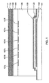
- Fig. 10 shows a representative example of a conventional single polarizer color LCD.
- a liquid crystal layer 206 is sandwiched between the substrate 201 and its facing transparent substrate 208.
- TN Transmission Nematic
- STN Super Twisted Nematic
- color filters 203a - 203f are formed corresponding to reflective electrodes 207a - 207f, and also striped transparent electrodes 205 are formed sandwiching protecting layer 204 in-between, and directing the stripes to a right angled direction with that of the stripes of the reflective electrodes 207a - 207f.
- a polarizer 211, a phase compensation plate 210 and a scattering plate 209 are laid bonded from outside in order.
- the single-polarizer reflective LCD provides a brighter display compared with the double-polarizer reflective LCD because the light passing frequency through the polarizer(s) decreases from four times to two times.
- the reflective electrodes 207a - 207f can be built in liquid crystal cells, so that a display of less parallax is obtainable.
- the single polarizer type can minimize the probability that incoming light and outgoing light pass through different color domains, which also provides a high color purity and brighter display.
- the plane surface of an electrode is desired.
- the reflective luminance except for certain directions becomes extremely small, so that a direct view reflective LCD cannot be realized as it is.
- a scattering plate 209 is disposed in a light propagation path.
- the optical system is so composed that the scattering function is separated from the reflection function.
- Al aluminum
- Al is used for the reflective electrodes 207a - 207f because Al is less expensive and has a high reflective characteristic of less wavelength dependence.
- the reflective electrodes 207a - 208f are exposed during cell assemble processes, the durability to an acid, alkali or a solvent is not sufficient, so that the corrosion by such chemicals are concerned.
- the reflective electrodes 207a - 207f contact directly with the liquid crystal, it is difficult to maintain durability against corrosion. Particularly, it is difficult to keep reliability in a constant-voltage loading test under high temperature and high humidity conditions.
- the above problems are especially liable to occur when Al is used.
- the present invention aims to provide, by relatively simple structure, a bright and less parallax reflective LCD which is also superior in processing and reliability.
- a reflective LCD according to the invention is defined in claim 1. It comprises a substrate, a transparent substrate facing the substrate, and a liquid crystal layer sandwiched between the substrate and the transparent substrate.
- the reflective LCD further comprises first transparent electrodes, an electrically insulating separating layer and a reflective film, which are formed in this order from the liquid crystal layer side at the inward-facing surface of the substrate.
- Second transparent electrodes are included in the inward-facing surface of the transparent substrate.
- the electrically insulating separating layer separates electrically and physically the reflective film from the first transparent electrodes.
- the surface of the reflective film is covered and protected by the separating layer, and the reflective surface is disposed in a liquid crystal cell, so that the feature of a single polarizer type is kept. This is superior in processing and reliability, is less parallax and results in a bright display.
- the first and the second transparent electrodes compose a group of transparent electrodes, or a single transparent electrode, or a group of pixel electrodes which are combined with active matrix array. Also by forming an additional insulating layer on the surface of the reflective film, durability against a solvent and corrosion is improved.
- the insulating layer can be formed by anodic oxidation of the reflective film.
- the insulating layer can also be composed by forming an insulating thin film on the surface of the reflective film by sputtering.
- the main composition of the reflective film can be A1.
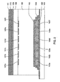
- a reflective film 102 of preferably Al is selectively formed at the domain nearly corresponding to a display part.
- an electrically insulating separating layer 120 is formed, and on that, a plurality of striped first transparent electrodes 105 are selectively formed.
- first transparent electrodes indium tin oxide (ITO) is used.
- ITO indium tin oxide
- the separating layer 120 is formed to insulate physically and electrically the reflective film 102 from the first transparent electrodes 105. If ITO and Al are electrically contacted, ITO is corroded by an electrochemical reaction when the patterning of ITO is made by wet etching. Such corrosion is suppressed by the structure described above.
- acrylic resin which has good transparency and is electrically insulating, is used.
- a liquid crystal layer 106 is sandwiched between the substrate 101 and its facing transparent substrate 108 made of glass or the like.
- a liquid crystal layer 106 STN liquid crystal is used for the liquid crystal layer 106.
- ITO for the striped second transparent electrodes 107a - 107f are selectively formed directing the stripes to a right-angled direction with that of stripes of the first transparent electrodes 105.
- a polarizer 111 At the outward-facing surface of transparent substrate 108, a polarizer 111, a phase compensation plate 110 and a scattering plate 109 are laid bonded from outside in order.
- the liquid crystal can be driven by applying electric potential between the first transparent electrodes 105 and the second transparent electrodes 107a - 107f. This is so-called single matrix driving.
- the durability against chemicals in the assembling process of liquid crystal cells is good because the reflective film 102 is covered by the separating layer 120, and also the reliability in constant-voltage loading test under high temperature and high humidity conditions are good.
- the reflective surface is disposed in the liquid crystal cell, so that a less parallax and high brightness monochrome reflective LCD is realized.
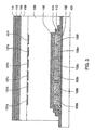
- Al for a reflective film 102 is selectively formed at the domain nearly corresponding to a display part.
- the first transparent layer 105 is selectively formed on them. Namely, the roll of the separating layer 120 in the first exemplary embodiment is played by the color filters 103 a - 103f and by the protecting layer 104, so that the corrosion caused by electrochemical reaction during the patterning process of the transparent electrode 105 is suppressed.
- the transparent electrode 105 indium tin oxide (ITO) is used.
- ITO indium tin oxide
- acrylic resin acrylic resin, which has good transparency and is electrically insulating, is used.
- a liquid crystal layer 106 is sandwiched between the substrate 101 and its facing transparent substrate 108.
- a liquid crystal layer 106 STN liquid crystal is used for the liquid crystal layer 106.
- second transparent electrodes 107a - 107f are selectively formed corresponding to the color filters 103a - 103f.
- a polarizer 111 At the outward-facing surface of the transparent substrate 108, a polarizer 111, a phase compensation plate 110 and a scattering plate 109 are laid bonded from outside in order.
- the liquid crystal can be driven by applying electric potential between the first transparent electrodes 105 and the second transparent electrodes 107a - 107f.
- the reflective film 102 is completely covered by the color filters 103 a - 103f and also by the protecting layer 104, scratching during the assembling process, as is seen in a conventional reflective electrode, hardly occurs and inspection and handling is easy.
- the process of forming the separating layer can be omitted.
- the reflective surface is disposed in the cell, so that a less parallax, higher brightness and higher color purity color reflective LCD is realized.
- a new insulating layer 112 is provided on the surface of a reflective film. Namely, as shown in Fig. 3, an insulating layer 112 is laid between the reflective film 102 and color filters 103a - 103f, and the whole surface of the reflecting film 102 is covered by the insulating layer 112.
- oxidized tantalum (TaOx) by sputtering is used for the insulating layer 112, then the durability of reflective film 102 against chemicals and corrosion is further improved.
- the reflective LCD of the third exemplary embodiment of the present invention referring to Fig. 3 showing a cross sectional view of the exemplary embodiment.
- the difference of this exemplary embodiment from the second exemplary embodiment is in the composition of an insulating layer 112.
- the insulating layer 112 in Fig. 3 is formed by anodic oxidation of Al which is used for a reflective film 102.
- oxidized aluminum is formed by anodic oxidation by setting the reflective film 102 as an electrode of one side in the mixed liquid of oxalic acid ammonium and ethylene glycol.
- the probability of occurrence of pinholes is extremely small from its principle, so that the isolation effect from a solvent and water is greatly improved. Therefore, the durability against chemicals and corrosion of the reflective film is further improved from that of the first exemplary embodiment.
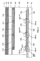
- Al for a reflective film 102 is selectively formed at the domain nearly corresponding to a display part.
- an electrically insulating separating layer 120 is formed, and on that, a plurality of striped first transparent electrodes 105a - 105f are selectively formed.
- first transparent electrodes 105a -105f indium tin oxide (ITO) is used.
- ITO indium tin oxide
- the separating layer 120 is formed to insulate electrically the reflective film 102 from the first transparent electrodes 105a - 105f.
- corrosion caused by electrochemical reaction at the time of patterning of the first transparent electrodes 105a -105f is suppressed.
- acrylic resin which has good transparency and is electrically insulating, is used.
- a liquid crystal layer 106 is sandwiched between the substrate 101 and its facing transparent substrate 108.
- a liquid crystal layer 106 STN liquid crystal is used for the liquid crystal layer 106.
- electrically insulating striped color filters 113a - 113f are selectively formed. Then, these are covered by a electrically insulating protecting layer 114, and then a plurality of striped second transparent electrodes 107 are selectively formed directing the stripes to a right angled direction with that of the stripes of the first transparent electrodes 105a - 105f. In case of necessity, black matrixes are added to the color filters.
- a polarizer 111 At the outward-facing surface of transparent substrate 108, a polarizer 111, a phase compensation plate 110 and a scattering plate 109 are laid bonded from outside in order.
- the liquid crystal can be driven by applying electric potential between the first transparent electrodes 105a - 105f and the second transparent electrodes 107.
- the feature of a single polarizer type is also kept, so that a less parallax and higher brightness color reflective LCD, which is also superior on durability against chemicals and corrosion, is realized.
- the first and the second transparent electrodes are striped and the plan view shows that the stripes are disposed to make a right angle with each other, and composes the domain corresponding to a display part.
- the example of so-called single matrix type is shown.
- the same effect is obtained even if the first or the second transparent electrode is a single transparent electrode which is flat all over the display part, that is a so called segment display type.
- the active matrix array means that pixels are disposed in a matrix and the each pixel is connected to address line via switch which is an active element.
- the voltage applied to each pixel is independently controlled by the switch, so that picture quality is not deteriorated by phenomena such as crosstalk compared with a single matrix type, then a higher quality and higher color purity display is obtainable in case of a color LCD.
- a thin film transistor TFT
- a plurality of pixel electrodes viz., first transparent electrodes 105a - 105 f (hereinafter abbreviated 105) are disposed in matrix, and each of the TFTs 137a - 137c (hereinafter abbreviated 137, marked “TFT” in the illustration) is connected to each pixel electrodes.
- first transparent electrodes ITO
- ITO indium tin oxide
- the TFT 137 comprises gate electrodes 132a - 132c (hereinafter abbreviated 132, marked “G” in the illustration), a gate-insulating film 133 formed on those and made of silicon nitride, semiconductors 134a etc made of hydrogenated amorphous silicon, source electrodes 135a - 135c (marked “S” in the illustration) which include molybdenum (Mo) alloy and drain electrodes 136a etc (marked “D” in the illustration). Between the semiconductor and the source or the drain electrodes, in some cases, in order to make a better electric contact, N-type impurities doped layer made of amorphous silicon which contains phosphorus is provided.
- the drain electrode 136a is connected to the first transparent electrode 105a.
- the gate electrodes 132 a - 132c in each row are connected to each other and form a gate address line.
- Source electrodes 135a - 135c in each column are connected to each other and form source address line.
- Al for reflective films 102a - 102c (hereinafter abbreviated 102) are selectively formed.
- a gate-insulating film 133 is formed on the reflective films 102.
- the first transparent electrode 105 is formed on that, the first transparent electrode 105 is formed. Therefore, the first transparent electrode 105 is insulated electrically and physically from the reflective films 102 by the gate-insulating film 133.
- the reflective films 102 and the gate electrodes 132 are formed at the same level, and the same material Al is used for the both, so that there is a merit of producing a reflective LCD without increasing the production process.
- a liquid crystal layer 106 is sandwiched between the substrate 101 and its facing transparent substrate 108.
- liquid crystal layer 106 TN liquid crystal, which suits for an active matrix array, is used.
- striped color filters 113a - 113c are selectively formed, which correspond to the first transparent electrodes 105 a - 105c. Then, at the space between each stripe of the color filters, black matrixes 131a - 131c are formed for the purpose of intercepting light.
- a second transparent electrode 107 is formed. In this exemplary embodiment, the second transparent electrode 107 is formed evenly all over the display domain.
- a polarizer 111 At the outward-facing surface of the transparent substrate 108, a polarizer 111, a phase compensating plate 110 and a scattering plate 109 are laid.
- the phase compensating plate 110 is not essential, but it is better to be adopted for increasing a viewing angle.
- the liquid crystal can be driven by applying electric potential between the first transparent electrodes 105 and the second transparent electrode 107.
- the voltages accurately corresponding to a display pattern can be applied. Namely, during the period when the gate voltage is "HIGH", the source electrode and the drain electrode become conductive with each other. Then the source voltage is transferred to pixel electrode viz., to the first transparent electrodes 105. Then, when the gate voltage becomes "LOW", the source electrode and the drain electrode are insulated for each other, so that the voltage, which is transferred to the transparent electrode 105 right before becoming the insulated state, is held until the gate voltage becomes "HIGH” next time. Then, as is well known, by properly controlling the voltage applied to the gate electrodes and the source electrode from outside driving circuit, the voltage which exactly corresponds to a display pattern can be applied to each pixel electrode.
- an active matrix array is formed on a substrate 101. Since the structure and the function of the active matrix array are the same as in the sixth exemplary embodiment, the explanation is omitted.
- the difference from the sixth exemplary embodiment is that an inter-layer insulating film 138 is newly provided on reflective films 102. Namely, in this exemplary embodiment, the reflective films 102 and gate electrodes 132 are formed at different levels, so that materials for gate electrodes 132 which are the composing elements of the gate array and that for the reflective films 102 can be selected independently. Then more suitable material for performing each function can be adopted and the reflective LCD of higher performance is realized. In Fig. 7, the reflective films 102 are separated by each pixel, however the film can be formed evenly all over the display domain to simplify the process.
- the surface of the reflective films 102 are covered by both inter-layer insulating film 138 and gate-insulating film 133, so that the effect of protecting the reflective films102 is high, and also the display quality can be further improved.
- an active matrix array is formed on a substrate 101.
- the structure is the same as in the sixth exemplary embodiment except that color filters 103a - 103c (hereinafter abbreviated 103) and black matrixes 131a - 131c are formed on the active matrix array in this exemplary embodiment, namely the structure of so called Color-Filter-on-Array (CFOA) is adopted in this embodiment.
- CFOA Color-Filter-on-Array
- pixel electrodes viz., the first transparent electrodes 105a - 105c (hereinafter abbreviated 105) are formed.
- the first transparent electrodes 105 and drain electrodes 136a etc are connected through contact window opened through the color filters.
- a protecting layer may be laid between the color filters 103 and the first transparent electrodes 105.
- Al for reflective films 102a - 102c (hereinafter abbreviated 102) is selectively formed.
- a gate-insulating film 133 is formed on the reflective films 102.
- color filters 103a - 103c and black matrixes 131a - 131c are formed on the first transparent electrodes 105, so that the first transparent electrodes 105 are completely separated electrically and physically from the reflective films 102.
- liquid crystal layer 106 is sandwiched between the substrate 101 and its facing transparent substrate 108.
- transparent liquid crystal layer 106 TN liquid crystal is used for the transparent liquid crystal layer 106.
- second transparent electrode 107 is formed.
- the second transparent electrode 107 is formed evenly all over the display domain.
- polarizer 111 At the outward-facing surface 108, polarizer 111, phase compensating plate 110 and scattering plate 109 are laid bonded.
- color filters are disposed on the substrate 101 which includes reflective films 102, so that the display quality is not deteriorated by parallax. Also, since the exact voltage is applied by active matrix, better quality display is realized, and also durability against chemicals and reliability are high.
- an active matrix array is formed at the side of a transparent substrate.
- Al for a reflective films 102 is selectively formed at the domain corresponding to a display part.
- a first transparent electrode 105 is formed on the reflective films 102.
- the first transparent electrode 105 is evenly formed all over the display domain.
- the color filters are covered by a protecting layer if necessary.
- the reflective films 102 are electrically insulated from the first transparent electrode 105 by the color filters 103a - 103c and by the black matrixes 131a - 131c, so that the corrosion caused by electrochemical reaction at the patterning process of the transparent electrode 105 is suppressed.
- a liquid crystal layer 106 is sandwiched between the substrate 101 and its facing transparent substrate 108.
- TN liquid crystal which suits for an active matrix array, is used.
- the active matrix array is formed at the inward-facing surface of the transparent substrate 108 and the color filters are provided at the side of the substrate 101.
- the structure is the same as in the third comparative example. Namely, as shown in Fig. 9, the active matrix array comprises gate electrodes 132a - 132c, a gate-insulating film 133, hydrogenated amorphous silicon semiconductors 134a - 134c, source electrodes 135a - 135c, and drain electrodes 136a - 136c. And, each drain electrode of each TFT is connected to each pixel electrode, viz., to each of second transparent electrodes 107a - 107c.
- the pixel electrodes, viz., the second transparent electrodes 107a - 107c are disposed at the positions corresponding to the color filters 103a - 103c which are formed on the substrate 101.
- a polarizer 111, phase compensating plate 110 and scattering plate 109 are laid bonded.
- the structure described above also provides a reflective color LCD which has the feature of a single polarizer type, and has a high display quality, high brightness and high color purity which are the features of active matrix, and also has features of superior processing, durability against chemicals and reliability.
- amorphous silicon TFT is used for the active element of the active matrix array.
- the active element is not limited to this.
- Polysilicon TFT is also usable.
- the gate electrodes are positioned under the semiconductor, namely it is the type called "bottom gate type". However, it can be "top gate type” in which the gate electrodes are positioned at upper side of the semiconductor or a coplanar type.
- a Metal-Insulator-Metal (MIM) type diode is also usable
- the reflective LCD of the present invention is that the liquid crystal is sandwiched between the substrate and its facing transparent substrate. And at the inward-facing surface of the substrate, the first transparent electrodes are formed, and also a separating layer or the same functional color filters or gate-insulating film, and the reflective film are formed. At the inward-facing surface of the transparent substrate, the second transparent electrodes are formed. And the reflective film is electrically and physically separated from the first transparent electrodes. The reflective surface of the reflective film is positioned inside the cell, so that the feature of a single polarizer type is kept.
- the reflective film is covered by the protecting layer, different from the conventional one, the scratching of the reflective film hardly occurs during the assembling process, and the inspection and the handling are easy, and also durability against chemicals and the reliability are superior. Also by combining with the active matrix, the reflective LCD of higher brightness and higher display quality, compared with conventional types, is realized.
Claims (4)
- Dispositif d'affichage à cristaux liquides à réflexion comprenant :dans lequel ladite couche de protection électriquement isolante et ladite couche de filtres colorés séparent physiquement et électriquement ledit film réfléchissant de ladite première électrode transparente.un substrat (101),un substrat transparent (108),une couche à cristaux liquides (106) entre ledit substrat et ledit substrat transparent,une première électrode transparente (105), une couche de protection électriquement isolante (104), une couche de filtres colorés (103), et un film conducteur réfléchissant (102) formés dans l'ordre entre ladite couche à cristaux liquides et ledit substrat, etune seconde électrode transparente (107) entre ledit substrat transparent et ladite couche de cristaux liquides,
- Dispositif d'affichage à cristaux liquides à réflexion selon la revendication 1, dans lequel ledit film réfléchissant comprend de l'aluminium.
- Dispositif d'affichage à cristaux liquides à réflexion selon la revendication 1 ou 2, dans lequel ladite couche de protection électriquement isolante est constituée d'une résine acrylique.
- Dispositif d'affichage à cristaux liquides à réflexion selon la revendication 2 ou 3, dans lequel ledit film réfléchissant qui comprend de l'aluminium est recouvert d'une couche isolante qui est formée par oxydation anodique dudit film réfléchissant.
Applications Claiming Priority (3)
| Application Number | Priority Date | Filing Date | Title |
|---|---|---|---|
| JP25120197 | 1997-09-17 | ||
| JP251201/97 | 1997-09-17 | ||
| JP25120197 | 1997-09-17 |
Publications (2)
| Publication Number | Publication Date |
|---|---|
| EP0903613A1 EP0903613A1 (fr) | 1999-03-24 |
| EP0903613B1 true EP0903613B1 (fr) | 2003-01-02 |
Family
ID=17219200
Family Applications (1)
| Application Number | Title | Priority Date | Filing Date |
|---|---|---|---|
| EP98117049A Expired - Lifetime EP0903613B1 (fr) | 1997-09-17 | 1998-09-09 | Dispositif d'affichage à cristaux liquides du type réflectif |
Country Status (7)
| Country | Link |
|---|---|
| US (1) | US6122027A (fr) |
| EP (1) | EP0903613B1 (fr) |
| JP (2) | JP3417312B2 (fr) |
| KR (1) | KR19990029903A (fr) |
| CN (1) | CN1198248C (fr) |
| DE (1) | DE69810408T2 (fr) |
| TW (1) | TW546512B (fr) |
Cited By (1)
| Publication number | Priority date | Publication date | Assignee | Title |
|---|---|---|---|---|
| US9348189B2 (en) | 2008-12-03 | 2016-05-24 | Semiconductor Energy Laboratory Co., Ltd. | Liquid crystal display device |
Families Citing this family (31)
| Publication number | Priority date | Publication date | Assignee | Title |
|---|---|---|---|---|
| JP3361451B2 (ja) * | 1998-03-24 | 2003-01-07 | 出光興産株式会社 | 反射型液晶表示装置用カラーフィルタ及びそれを用いた反射型液晶表示装置 |
| JP3326794B2 (ja) * | 1998-04-08 | 2002-09-24 | セイコーエプソン株式会社 | 液晶装置及び電子機器 |
| JP3085530B2 (ja) * | 1998-11-18 | 2000-09-11 | 日本電気株式会社 | 液晶表示装置及びその製造方法 |
| TW548484B (en) * | 1999-07-16 | 2003-08-21 | Seiko Epson Corp | Liquid crystal display device, electronic apparatus and substrate for liquid crystal device |
| CN1160592C (zh) * | 1999-11-24 | 2004-08-04 | 西铁城时计株式会社 | 液晶显示装置 |
| JP4717231B2 (ja) * | 2001-02-26 | 2011-07-06 | オプトレックス株式会社 | 反射型液晶表示パネル用マザー基板 |
| KR100790352B1 (ko) * | 2001-05-22 | 2008-01-02 | 엘지.필립스 엘시디 주식회사 | 반사형과 반사투과형 액정표시장치와 그 제조방법 |
| JP2003090997A (ja) * | 2001-07-13 | 2003-03-28 | Seiko Epson Corp | カラーフィルタ基板及び電気光学装置、カラーフィルタ基板の製造方法及び電気光学装置の製造方法並びに電子機器 |
| JP3873827B2 (ja) * | 2001-07-26 | 2007-01-31 | セイコーエプソン株式会社 | 液晶装置及び電子機器 |
| JP3610967B2 (ja) * | 2001-07-27 | 2005-01-19 | セイコーエプソン株式会社 | 電気光学装置、カラーフィルタ基板及び電子機器 |
| TW574533B (en) * | 2001-10-23 | 2004-02-01 | Au Optronics Corp | Liquid crystal display device structure |
| TWI227340B (en) * | 2002-02-25 | 2005-02-01 | Himax Tech Inc | Color filter and liquid crystal display |
| JP4237442B2 (ja) * | 2002-03-01 | 2009-03-11 | 株式会社半導体エネルギー研究所 | 半透過型液晶表示装置 |
| JP4101533B2 (ja) * | 2002-03-01 | 2008-06-18 | 株式会社半導体エネルギー研究所 | 半透過型の液晶表示装置の作製方法 |
| JP4087620B2 (ja) * | 2002-03-01 | 2008-05-21 | 株式会社半導体エネルギー研究所 | 液晶表示装置の作製方法 |
| CN1665678A (zh) * | 2002-05-08 | 2005-09-07 | 目标技术有限公司 | 银合金薄膜反射器和透明导电体 |
| JP2004295090A (ja) * | 2003-03-11 | 2004-10-21 | Seiko Instruments Inc | カラー液晶表示装置とその製造方法、およびカラーフィルタ基板の製造方法 |
| KR101007719B1 (ko) | 2003-07-31 | 2011-01-13 | 삼성전자주식회사 | 컬러필터기판 및 이를 갖는 액정표시장치 |
| JP4428330B2 (ja) * | 2005-09-28 | 2010-03-10 | エプソンイメージングデバイス株式会社 | 電気光学装置、および電子機器 |
| JP2007140565A (ja) * | 2007-02-23 | 2007-06-07 | Kyocera Corp | 液晶表示装置 |
| JP2011002855A (ja) * | 2010-09-22 | 2011-01-06 | Semiconductor Energy Lab Co Ltd | 液晶表示装置 |
| TWI490830B (zh) * | 2011-03-22 | 2015-07-01 | 群創光電股份有限公司 | 顯示模組及應用其之顯示器 |
| CN103700688B (zh) * | 2013-12-23 | 2016-03-30 | 京东方科技集团股份有限公司 | 彩膜基板及其制作方法、显示装置 |
| CN104614891B (zh) * | 2015-02-17 | 2018-05-01 | 深圳市华星光电技术有限公司 | 反射式柔性液晶显示器 |
| US9964799B2 (en) | 2015-03-17 | 2018-05-08 | Semiconductor Energy Laboratory Co., Ltd. | Display device, display module, and electronic device |
| CN104965358A (zh) * | 2015-07-14 | 2015-10-07 | 深圳市华星光电技术有限公司 | 反射式tft阵列面板及其制备方法和液晶显示器 |
| KR102401621B1 (ko) * | 2015-07-23 | 2022-05-25 | 삼성디스플레이 주식회사 | 액정 표시 장치 및 그 제조 방법 |
| WO2017195323A1 (fr) * | 2016-05-12 | 2017-11-16 | シャープ株式会社 | Dispositif d'affichage à cristaux liquides |
| CN107861287B (zh) * | 2017-12-13 | 2020-06-26 | 京东方科技集团股份有限公司 | 显示面板、显示装置及显示面板的制备方法 |
| KR20200041493A (ko) | 2018-10-12 | 2020-04-22 | 현대위아 주식회사 | 에어분사 기능을 갖는 공작기계용 와이퍼 |
| KR20210054154A (ko) | 2019-11-05 | 2021-05-13 | 현대위아 주식회사 | 공작기계용 도어 |
Family Cites Families (14)
| Publication number | Priority date | Publication date | Assignee | Title |
|---|---|---|---|---|
| JPS60133423A (ja) * | 1983-12-21 | 1985-07-16 | Seikosha Co Ltd | 液晶を利用した多色表示装置 |
| JPS61275728A (ja) * | 1985-05-02 | 1986-12-05 | Sumitomo Chem Co Ltd | カラ−液晶表示パネル |
| JPS62262826A (ja) * | 1986-05-09 | 1987-11-14 | Sharp Corp | 液晶式防眩ミラ− |
| US5058997A (en) * | 1989-08-11 | 1991-10-22 | International Business Machines Corporation | Tft lcd with optical interference color filters |
| US5079214A (en) * | 1990-10-11 | 1992-01-07 | Eastman Kodak Company | Patterned receiver for color filter array |
| JP3268858B2 (ja) * | 1992-11-30 | 2002-03-25 | 三洋電機株式会社 | 液晶表示装置 |
| CA2123658C (fr) * | 1993-05-19 | 1999-01-19 | Willis H. Smith, Jr. | Procede permettant d'obtenir une orientation parallele de cristaux liquides |
| MY114271A (en) * | 1994-05-12 | 2002-09-30 | Casio Computer Co Ltd | Reflection type color liquid crystal display device |
| JPH07321328A (ja) * | 1994-05-27 | 1995-12-08 | Hitachi Ltd | 薄膜トランジスタ駆動液晶表示装置およびその製法 |
| US5936693A (en) * | 1994-09-27 | 1999-08-10 | Casio Computer Co., Ltd. | Liquid crystal display device having a wide view angle |
| JPH08122767A (ja) * | 1994-10-28 | 1996-05-17 | Nec Kagoshima Ltd | カラー液晶ディスプレイ |
| JPH09236826A (ja) * | 1995-09-28 | 1997-09-09 | Sharp Corp | 液晶表示素子およびその製造方法 |
| JP3351945B2 (ja) * | 1995-12-18 | 2002-12-03 | シャープ株式会社 | 反射型液晶表示装置 |
| US6008872A (en) * | 1998-03-13 | 1999-12-28 | Ois Optical Imaging Systems, Inc. | High aperture liquid crystal display including thin film diodes, and method of making same |
-
1998
- 1998-09-09 EP EP98117049A patent/EP0903613B1/fr not_active Expired - Lifetime
- 1998-09-09 DE DE69810408T patent/DE69810408T2/de not_active Expired - Fee Related
- 1998-09-16 TW TW087115419A patent/TW546512B/zh not_active IP Right Cessation
- 1998-09-17 KR KR1019980038470A patent/KR19990029903A/ko not_active Application Discontinuation
- 1998-09-17 JP JP26257998A patent/JP3417312B2/ja not_active Expired - Lifetime
- 1998-09-17 CN CNB981195148A patent/CN1198248C/zh not_active Expired - Lifetime
- 1998-09-17 US US09/156,308 patent/US6122027A/en not_active Expired - Lifetime
-
2002
- 2002-06-06 JP JP2002165795A patent/JP2003075830A/ja active Pending
Cited By (1)
| Publication number | Priority date | Publication date | Assignee | Title |
|---|---|---|---|---|
| US9348189B2 (en) | 2008-12-03 | 2016-05-24 | Semiconductor Energy Laboratory Co., Ltd. | Liquid crystal display device |
Also Published As
| Publication number | Publication date |
|---|---|
| TW546512B (en) | 2003-08-11 |
| JP2003075830A (ja) | 2003-03-12 |
| DE69810408T2 (de) | 2003-09-25 |
| US6122027A (en) | 2000-09-19 |
| EP0903613A1 (fr) | 1999-03-24 |
| CN1222718A (zh) | 1999-07-14 |
| JPH11160698A (ja) | 1999-06-18 |
| DE69810408D1 (de) | 2003-02-06 |
| KR19990029903A (ko) | 1999-04-26 |
| JP3417312B2 (ja) | 2003-06-16 |
| CN1198248C (zh) | 2005-04-20 |
Similar Documents
| Publication | Publication Date | Title |
|---|---|---|
| EP0903613B1 (fr) | Dispositif d'affichage à cristaux liquides du type réflectif | |
| US6335771B1 (en) | Liquid crystal display device, and methods of manufacturing and driving same | |
| US5608556A (en) | Liquid crystal display having orientation control electrodes for controlling liquid crystal orientation | |
| US9030633B2 (en) | Driving method of liquid crystal display device | |
| US8314913B2 (en) | Liquid crystal display with subpixels having alternately disposed branches | |
| US6466290B2 (en) | Fringe field switching mode LCD | |
| KR100741890B1 (ko) | 횡전계 방식의 액정표시장치 및 그의 제조방법 | |
| US7483087B2 (en) | In-plane switching mode liquid crystal display device with heating line and method thereof | |
| KR100836495B1 (ko) | 액정표시장치 및 그 구동방법 | |
| US7619608B2 (en) | Electrophoretic display device | |
| KR20080050851A (ko) | 액정표시패널 | |
| US6052168A (en) | Active matrix liquid-crystal display with verticle alignment, positive anisotropy and opposing electrodes below pixel electrode | |
| TW200405071A (en) | Transflective liquid crystal device and electronic apparatus using the same | |
| US7220992B2 (en) | Thin film transistor array panel and a liquid crystal display including the same | |
| US7110069B2 (en) | Liquid crystal display with two surface display function | |
| KR20050001953A (ko) | 액정표시장치 및 그의 제조방법 | |
| US7253855B2 (en) | Liquid crystal display devices using a plastic substrate with particular relative thickness | |
| US7012662B2 (en) | Transflective LCD with twist angle less than 90 degrees and 4 compensation films | |
| KR20110080627A (ko) | 액정 표시 장치 | |
| JP3054042B2 (ja) | 反強誘電性液晶素子およびその駆動方法 | |
| US6734939B2 (en) | Array substrate for liquid crystal display device | |
| US6348959B1 (en) | Reflective LCD with dark borders | |
| US8427616B2 (en) | Bistable chiral splay nematic mode crystal display device | |
| US20090207116A1 (en) | Liquid crystal display | |
| KR20080098882A (ko) | 액정 표시 장치 |
Legal Events
| Date | Code | Title | Description |
|---|---|---|---|
| PUAI | Public reference made under article 153(3) epc to a published international application that has entered the european phase |
Free format text: ORIGINAL CODE: 0009012 |
|
| AK | Designated contracting states |
Kind code of ref document: A1 Designated state(s): DE FR GB |
|
| AX | Request for extension of the european patent |
Free format text: AL;LT;LV;MK;RO;SI |
|
| 17P | Request for examination filed |
Effective date: 19990601 |
|
| AKX | Designation fees paid |
Free format text: DE FR GB |
|
| 17Q | First examination report despatched |
Effective date: 20010122 |
|
| GRAG | Despatch of communication of intention to grant |
Free format text: ORIGINAL CODE: EPIDOS AGRA |
|
| GRAG | Despatch of communication of intention to grant |
Free format text: ORIGINAL CODE: EPIDOS AGRA |
|
| GRAH | Despatch of communication of intention to grant a patent |
Free format text: ORIGINAL CODE: EPIDOS IGRA |
|
| GRAH | Despatch of communication of intention to grant a patent |
Free format text: ORIGINAL CODE: EPIDOS IGRA |
|
| GRAA | (expected) grant |
Free format text: ORIGINAL CODE: 0009210 |
|
| AK | Designated contracting states |
Kind code of ref document: B1 Designated state(s): DE FR GB |
|
| PG25 | Lapsed in a contracting state [announced via postgrant information from national office to epo] |
Ref country code: FR Free format text: LAPSE BECAUSE OF FAILURE TO SUBMIT A TRANSLATION OF THE DESCRIPTION OR TO PAY THE FEE WITHIN THE PRESCRIBED TIME-LIMIT Effective date: 20030102 |
|
| REG | Reference to a national code |
Ref country code: GB Ref legal event code: FG4D Free format text: 20030102 |
|
| REF | Corresponds to: |
Ref document number: 69810408 Country of ref document: DE Date of ref document: 20030206 Kind code of ref document: P |
|
| PLBE | No opposition filed within time limit |
Free format text: ORIGINAL CODE: 0009261 |
|
| STAA | Information on the status of an ep patent application or granted ep patent |
Free format text: STATUS: NO OPPOSITION FILED WITHIN TIME LIMIT |
|
| EN | Fr: translation not filed | ||
| 26N | No opposition filed |
Effective date: 20031003 |
|
| REG | Reference to a national code |
Ref country code: GB Ref legal event code: 732E |
|
| PGFP | Annual fee paid to national office [announced via postgrant information from national office to epo] |
Ref country code: GB Payment date: 20080910 Year of fee payment: 11 |
|
| PGFP | Annual fee paid to national office [announced via postgrant information from national office to epo] |
Ref country code: DE Payment date: 20080926 Year of fee payment: 11 |
|
| GBPC | Gb: european patent ceased through non-payment of renewal fee |
Effective date: 20090909 |
|
| PG25 | Lapsed in a contracting state [announced via postgrant information from national office to epo] |
Ref country code: DE Free format text: LAPSE BECAUSE OF NON-PAYMENT OF DUE FEES Effective date: 20100401 |
|
| PG25 | Lapsed in a contracting state [announced via postgrant information from national office to epo] |
Ref country code: GB Free format text: LAPSE BECAUSE OF NON-PAYMENT OF DUE FEES Effective date: 20090909 |