EP0903565A1 - Integriertes abstimmbares Fabry-Pérot-Interferometer - Google Patents
Integriertes abstimmbares Fabry-Pérot-Interferometer Download PDFInfo
- Publication number
- EP0903565A1 EP0903565A1 EP98402302A EP98402302A EP0903565A1 EP 0903565 A1 EP0903565 A1 EP 0903565A1 EP 98402302 A EP98402302 A EP 98402302A EP 98402302 A EP98402302 A EP 98402302A EP 0903565 A1 EP0903565 A1 EP 0903565A1
- Authority
- EP
- European Patent Office
- Prior art keywords
- mirror
- control electrodes
- substrate
- interferometer
- mirrors
- Prior art date
- Legal status (The legal status is an assumption and is not a legal conclusion. Google has not performed a legal analysis and makes no representation as to the accuracy of the status listed.)
- Granted
Links
- 239000000758 substrate Substances 0.000 claims description 33
- 229910052710 silicon Inorganic materials 0.000 claims description 16
- 239000010703 silicon Substances 0.000 claims description 16
- 238000000034 method Methods 0.000 claims description 13
- 239000012528 membrane Substances 0.000 claims description 11
- 238000005530 etching Methods 0.000 claims description 9
- 238000004519 manufacturing process Methods 0.000 claims description 6
- 238000006073 displacement reaction Methods 0.000 claims description 5
- 229910052751 metal Inorganic materials 0.000 claims description 2
- 239000002184 metal Substances 0.000 claims description 2
- 239000011347 resin Substances 0.000 description 15
- 229920005989 resin Polymers 0.000 description 15
- XUIMIQQOPSSXEZ-UHFFFAOYSA-N Silicon Chemical compound [Si] XUIMIQQOPSSXEZ-UHFFFAOYSA-N 0.000 description 12
- 229910004298 SiO 2 Inorganic materials 0.000 description 7
- 238000000206 photolithography Methods 0.000 description 5
- 238000000151 deposition Methods 0.000 description 4
- VYZAMTAEIAYCRO-UHFFFAOYSA-N Chromium Chemical compound [Cr] VYZAMTAEIAYCRO-UHFFFAOYSA-N 0.000 description 3
- GRYLNZFGIOXLOG-UHFFFAOYSA-N Nitric acid Chemical compound O[N+]([O-])=O GRYLNZFGIOXLOG-UHFFFAOYSA-N 0.000 description 3
- 230000008021 deposition Effects 0.000 description 3
- 239000000203 mixture Substances 0.000 description 3
- 238000004088 simulation Methods 0.000 description 3
- CURLTUGMZLYLDI-UHFFFAOYSA-N Carbon dioxide Chemical compound O=C=O CURLTUGMZLYLDI-UHFFFAOYSA-N 0.000 description 2
- LFQSCWFLJHTTHZ-UHFFFAOYSA-N Ethanol Chemical compound CCO LFQSCWFLJHTTHZ-UHFFFAOYSA-N 0.000 description 2
- 238000010586 diagram Methods 0.000 description 2
- 239000003989 dielectric material Substances 0.000 description 2
- 238000004868 gas analysis Methods 0.000 description 2
- PCHJSUWPFVWCPO-UHFFFAOYSA-N gold Chemical compound [Au] PCHJSUWPFVWCPO-UHFFFAOYSA-N 0.000 description 2
- 239000010931 gold Substances 0.000 description 2
- 229910052737 gold Inorganic materials 0.000 description 2
- 229910017604 nitric acid Inorganic materials 0.000 description 2
- 230000003287 optical effect Effects 0.000 description 2
- 238000007789 sealing Methods 0.000 description 2
- UKFWSNCTAHXBQN-UHFFFAOYSA-N ammonium iodide Chemical compound [NH4+].[I-] UKFWSNCTAHXBQN-UHFFFAOYSA-N 0.000 description 1
- 238000000137 annealing Methods 0.000 description 1
- 229910002092 carbon dioxide Inorganic materials 0.000 description 1
- 239000001569 carbon dioxide Substances 0.000 description 1
- 229910000355 cerium(IV) sulfate Inorganic materials 0.000 description 1
- 229910052804 chromium Inorganic materials 0.000 description 1
- 239000011651 chromium Substances 0.000 description 1
- 239000007789 gas Substances 0.000 description 1
- XLYOFNOQVPJJNP-ZSJDYOACSA-N heavy water Substances [2H]O[2H] XLYOFNOQVPJJNP-ZSJDYOACSA-N 0.000 description 1
- 238000009413 insulation Methods 0.000 description 1
- 239000012212 insulator Substances 0.000 description 1
- 238000005305 interferometry Methods 0.000 description 1
- 238000003754 machining Methods 0.000 description 1
- 238000001465 metallisation Methods 0.000 description 1
- 238000005459 micromachining Methods 0.000 description 1
- 230000003071 parasitic effect Effects 0.000 description 1
- 230000002093 peripheral effect Effects 0.000 description 1
- 238000000926 separation method Methods 0.000 description 1
- 230000000391 smoking effect Effects 0.000 description 1
- 125000006850 spacer group Chemical group 0.000 description 1
Images


Classifications
-
- G—PHYSICS
- G01—MEASURING; TESTING
- G01J—MEASUREMENT OF INTENSITY, VELOCITY, SPECTRAL CONTENT, POLARISATION, PHASE OR PULSE CHARACTERISTICS OF INFRARED, VISIBLE OR ULTRAVIOLET LIGHT; COLORIMETRY; RADIATION PYROMETRY
- G01J3/00—Spectrometry; Spectrophotometry; Monochromators; Measuring colours
- G01J3/12—Generating the spectrum; Monochromators
- G01J3/26—Generating the spectrum; Monochromators using multiple reflection, e.g. Fabry-Perot interferometer, variable interference filters
-
- G—PHYSICS
- G02—OPTICS
- G02B—OPTICAL ELEMENTS, SYSTEMS OR APPARATUS
- G02B26/00—Optical devices or arrangements for the control of light using movable or deformable optical elements
- G02B26/001—Optical devices or arrangements for the control of light using movable or deformable optical elements based on interference in an adjustable optical cavity
Definitions
- the invention relates to the field of interferometry, and more particularly the production of a Fabry-Pérot interferometer, electrostatically controllable and tunable.
- Such device is for example used as a filter interferometric.
- EP-668,490 and EP 693,683 describe integrated Fabry-Pérot interferometers, to order electrostatic.
- a resonant optical cavity is machined in a silicon substrate.
- This cavity is an air layer of thickness ⁇ / 2, ⁇ being the working wavelength, which is machined between two parallel dielectric mirrors.
- One of the mirrors is mobile, while the other remains fixed.
- Each of these mirrors carries control electrodes, which can be produced in the form of conductive deposits of highly doped silicon layers. The application of a potential difference between these control electrodes attracts the movable mirror towards the fixed mirror, thus modifying the air thickness, and therefore the resonance wavelength.
- the electrode of the mirror mobile is annular and machining an area thinner around the mirror makes the center of it more rigid, and improves the plane displacement of the area useful central optics.
- the devices described in these various documents use mounted control electrodes by the two parallel mirrors.
- the command electrostatic is done directly by application of a voltage on these electrodes.
- This technique requires making electrical contacts out of two conductive faces opposite, hence a certain complexity of the resulting device, and of the process allowing to realize it.
- taking contact on the upper mirror is delicate, and requires local stacking of layers strongly doped. Very great attention must therefore be paid on the insulation of the different active parts, so avoid any short circuit.
- the electrode associated with one of the mirrors is a floating electrode
- no socket contact is not to be made on the side of this mirror.
- the interferometer according to the invention is still electrostatic, but both control electrodes are brought to one side of the device.
- the floating electrode and the mirror to which it is associated can be made on the surface of a first substrate.
- this substrate is made of silicon and the floating electrode is made of doped silicon.
- the other mirror, and its control electrodes can be made on the surface of a second substrate, for example, too, made of silicon.
- the mobile mirror can consist of an engraved membrane in a substrate.
- control electrodes they can be formed on either side of an area reflective with which they are associated, by example the mobile mirror.
- this mirror has a reflective central zone and zones side on which the electrodes are placed control.
- This central reflective area can have a circular shape.
- this circular shape delimited by control electrodes, allows movement perfectly plan of the moving reflective area, since the electrostatic attraction only takes place at the periphery of this area, which allows to have a diaphragm filter outlet.
- Control electrodes can be realized in a metallic deposit.
- contacts can be taken directly from the control electrodes, on the surface of one of the substrates.
- the floating electrode and the mirror corresponding can be made on the surface of a first substrate.
- the substrate can be in silicon and the floating electrode can be realized by doping a thin layer of silicon on the surface of the first mirror formed from at least one layer dielectric, first mirror deposited itself on the substrate.
- the floating electrode can also be produced by a metal deposit placed on the mirror.
- the other mirror, as well as the first and second control electrodes can be made in surface of a second substrate.
- this second mirror consists of a membrane, part of which (the mobile reflective zone) is made mobile by etching of the second substrate.
- control electrodes on the other hand, can be made by metallic deposition on one of the mirrors.
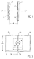
- Figure 1 shows the structure of a tunable Fabry-Pérot interferometer controlled electrostatically, according to the invention.
- This structure comprises a first fixed mirror 4, with which a floating electrode 2 is associated.
- the fixed mirror 4 is formed for example on a substrate.
- the floating electrode 2 is produced on the surface of the mirror 4.
- This mirror 4 consists of a stack of layers of different dielectrics (for example SiO 2 and Si undoped; or else at least one layer of SiO 2 and one layer of undoped Si, the undoped Si being a dielectric).
- the floating electrode may be the last layer of the stack forming the mirror, it then consists of doped silicon, therefore conductive.
- Facing the fixed mirror 2 is a second mirror 6, mobile, along an axis XX 'of the interferometer.
- Two second control electrodes 8, 10 are associated with this second mirror. These are for example produced by metallization of part of a reflecting membrane forming the second mirror 6.
- the two mirrors are held one relative to the other at a distance d. This distance is actually the length of the resonant cavity defined by the mirrors 4, 6.
- Keeping the two mirrors at a distance d is made using, for example, sleepers or stops, or spacers not shown in the figure 1.
- the cavity thus formed defines, from the electrical point of view, a capacitance C 1 between the control electrodes 8, 10 and the floating electrode 2.
- the application of an electric voltage between the control electrodes modifies, through the capacitance C 1 of the air gap, the potential of the floating electrode 2, and thus the movable mirror 6 is attracted towards the fixed mirror.
- control electrodes 8, 10 are made by metallic deposition on a surface, or membrane, reflective.
- the metallic deposit leaves a circular opening 12 on the surface reflective, thus leaving a central area free, reflective and mobile.
- the deposit leaves two free trenches 14, 16 used to isolate the electrodes of command 8, 10 relative to each other.
- the electrodes can be produced by metallic deposition then by etching of zones 12, 14, 16.
- FIG. 3 An embodiment of an interferometer according to the invention is illustrated in FIG. 3.
- This interferometer is produced in two substrates 20, 22, for example in silicon of SOI type ("Silicon On Insulator").
- Mirrors 32, 26 are produced by depositing thin layers: these are for example deposits made up of a stack of different dielectrics, for example SiO 2 and Si (the undoped Si is a dielectric), of thickness ⁇ / 4, alternating and produced on each of the faces 28, 30 of the two substrates intended to be opposite one another.
- the thickness and the number of layers of each stack to be deposited depends on the wavelength at which the filter, or the interferometer, is intended to resonate, as well as on the desired emission finesse.
- the outer layer 24 of the stack is formed of doped silicon to make it conductive.
- the two mirrors 32, 26 define a cavity Fabry-Pérot whose resonance wavelengths are defined by equation (1) above, the distance d being the distance between the surfaces of the two mirrors.
- the fixed mirror 32 is provided with an electrode, called floating, 24.
- the mirror 26 is provided with two electrodes 38, 40, for example having the form described above in conjunction with Figure 2. At these electrodes associated with electrical contacts. Two cavities 42, 44 etched in the substrate 22 possibly allow to leave a passage for these electrical contacts.
- the floating electrode can be produced by example by strong doping of the substrate 22.
- Maintaining the two substrates, one relative to the other, in the desired position so as to define a Fabry-Pérot cavity of length d, is provided by stops 46, 48 and by sealing with seals, or resin pads 50, 52.
- seals, or resin pads 50, 52 Preferably, we leave in the resin joints of the vents which allow equalize the pressures inside and outside the Fabry-Pérot cavity.
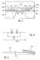
- FIG. 4 represents an electrical diagram equivalent to the overall structure, where C 1 denotes the control capacitance produced between the control electrode and the floating electrode, and where C 2 denotes the parasitic capacitance, due for example, in the mode of FIG. 2, in the trenches 14, 16. Still taking the example of FIG.
- This simulation was carried out using the finite element method (ANSYS).
- FIG. 5 illustrates the result: it represents only half of the membrane (mobile central zone 54 and metallized peripheral zone 56), the arrows representing the zone where the electrostatic force is applied.
- the deflection ⁇ obtained is 0.32 ⁇ m.
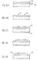
- FIGS. 6A to 6M represent stages of realization of a device according to the invention.
- FIGS. 6A to 6F represent the steps of realization of a first part of the interferometer.
- a substrate 60 for example of the SOI type, with a deposit 62 of SiO 2 on the front face.
- the reference 64 also designates an SiO 2 layer. Between the two is a layer 63 of Si.
- a photolithography step is then carried out: a positive resin is spread on the substrate ("schipley 1828" type resin), which is dried.
- An insolation step makes it possible to define the shape of the separation stops (FIG. 6B: stops 46, 48 of FIG. 3).
- Development is then carried out, that is to say the removal of the insolated resin, then annealing.
- the engraving of the stops can be performed at CHF 3 / O 2 and the removal of the resin with fuming nitric acid.
- the next step is a step of etching the Si 3 N 4 front face by photolithography of positive resin (to define the cavities 42, 44), etching with CHF 3 / O 2 and removal of the resin with HNO 3 smoking.
- the Si 3 N 4 is removed on the front panel by etching the CHF 3 / O 2 .
- Figures 6G to 6L show stages of realization of a second part of an interferometer.
- An opening 76 is made in the rear resin layer (FIG. 6J), by photolithography with positive resin, etching of the rear face of Si 3 N 4 at CHF 3 / O 2 and removal of the resin with fuming HNO 3 .
- the front layer 74 of Si 3 N 4 is etched at CHF 3 / O 2 in order to release the control electrodes.
- the floating electrode is associated to the moving mirror, this is the substrate on which this electrode is made which is etched, not the substrate on which the electrodes are made ordered.
- the interferometer according to the invention is tunable and can be integrated into any gas analysis system which requires a wavelength selection. His tunable nature makes it possible to detect several gases, depending on the wavelength of job. It is also possible to work in optical frequency modulation.
- the interferometer according to the invention can be used for telecommunications, because micro-machining of silicon allows very small cavities, and therefore resonances around the lengths wave at 1.3 ⁇ m and 1.55 ⁇ m.
Landscapes
- Physics & Mathematics (AREA)
- Spectroscopy & Molecular Physics (AREA)
- General Physics & Mathematics (AREA)
- Optics & Photonics (AREA)
- Mechanical Light Control Or Optical Switches (AREA)
- Spectrometry And Color Measurement (AREA)
- Micromachines (AREA)
Applications Claiming Priority (2)
| Application Number | Priority Date | Filing Date | Title |
|---|---|---|---|
| FR9711696A FR2768812B1 (fr) | 1997-09-19 | 1997-09-19 | Interferometre fabry-perot accordable integre |
| FR9711696 | 1997-09-19 |
Publications (2)
| Publication Number | Publication Date |
|---|---|
| EP0903565A1 true EP0903565A1 (de) | 1999-03-24 |
| EP0903565B1 EP0903565B1 (de) | 2004-06-02 |
Family
ID=9511271
Family Applications (1)
| Application Number | Title | Priority Date | Filing Date |
|---|---|---|---|
| EP98402302A Expired - Lifetime EP0903565B1 (de) | 1997-09-19 | 1998-09-17 | Integriertes abstimmbares Fabry-Pérot-Interferometer |
Country Status (5)
| Country | Link |
|---|---|
| US (1) | US6078395A (de) |
| EP (1) | EP0903565B1 (de) |
| JP (1) | JP4578587B2 (de) |
| DE (1) | DE69824249T2 (de) |
| FR (1) | FR2768812B1 (de) |
Cited By (1)
| Publication number | Priority date | Publication date | Assignee | Title |
|---|---|---|---|---|
| WO2001059415A1 (fr) * | 2000-02-14 | 2001-08-16 | Schlumberger Industries, S.A. | Filtre fabry-perot court a couches metalliques |
Families Citing this family (50)
| Publication number | Priority date | Publication date | Assignee | Title |
|---|---|---|---|---|
| FI981456A0 (fi) * | 1998-06-24 | 1998-06-24 | Valtion Teknillinen | Menetelmä mikromekaanisten elektrodien välisen etäisyyden sähköiseksi säätämiseksi |
| US6295130B1 (en) * | 1999-12-22 | 2001-09-25 | Xerox Corporation | Structure and method for a microelectromechanically tunable fabry-perot cavity spectrophotometer |
| US6608711B2 (en) * | 2000-03-03 | 2003-08-19 | Axsun Technologies, Inc. | Silicon on insulator optical membrane structure for fabry-perot MOEMS filter |
| US6341039B1 (en) | 2000-03-03 | 2002-01-22 | Axsun Technologies, Inc. | Flexible membrane for tunable fabry-perot filter |
| US6836366B1 (en) | 2000-03-03 | 2004-12-28 | Axsun Technologies, Inc. | Integrated tunable fabry-perot filter and method of making same |
| US6373632B1 (en) | 2000-03-03 | 2002-04-16 | Axsun Technologies, Inc. | Tunable Fabry-Perot filter |
| US6597461B1 (en) | 2000-03-20 | 2003-07-22 | Parvenu, Inc. | Tunable fabry-perot interferometer using entropic materials |
| US6665109B2 (en) | 2000-03-20 | 2003-12-16 | Np Photonics, Inc. | Compliant mechanism and method of forming same |
| US6747775B2 (en) * | 2000-03-20 | 2004-06-08 | Np Photonics, Inc. | Detunable Fabry-Perot interferometer and an add/drop multiplexer using the same |
| US6678084B2 (en) | 2000-03-20 | 2004-01-13 | Np Photonics, Inc. | Methods of making mechanisms in which relative locations of elements are maintained during manufacturing |
| AU2001249289A1 (en) | 2000-03-20 | 2001-10-03 | Solus Micro Technologies, Inc. | Electrostatically-actuated tunable optical components using entropic materials |
| US6747784B2 (en) | 2000-03-20 | 2004-06-08 | Np Photonics, Inc. | Compliant mechanism and method of forming same |
| US6356689B1 (en) * | 2000-03-25 | 2002-03-12 | Lucent Technologies, Inc. | Article comprising an optical cavity |
| US6538748B1 (en) * | 2000-04-14 | 2003-03-25 | Agilent Technologies, Inc | Tunable Fabry-Perot filters and lasers utilizing feedback to reduce frequency noise |
| US6400738B1 (en) * | 2000-04-14 | 2002-06-04 | Agilent Technologies, Inc. | Tunable Fabry-Perot filters and lasers |
| US6721098B2 (en) | 2000-12-22 | 2004-04-13 | Axsun Technologies, Inc. | Triple electrode MOEMS tunable filter and fabrication process therefor |
| US7425453B1 (en) * | 2001-03-14 | 2008-09-16 | The United States Of America As Represented By The Secretary Of The Navy | Integrated circuit porphyrin-based optical Fabry-Perot chemical sensor |
| JP4720022B2 (ja) * | 2001-05-30 | 2011-07-13 | ソニー株式会社 | 光学多層構造体およびその製造方法、光スイッチング素子、並びに画像表示装置 |
| KR100411328B1 (ko) * | 2001-12-21 | 2003-12-18 | 한국과학기술원 | 가변 광학 필터 |
| KR100453975B1 (ko) * | 2002-10-25 | 2004-10-20 | 전자부품연구원 | 초소형 자기력 구동 패브리-페롯 필터 및 그를 이용한가스 분석 장치 |
| US6996312B2 (en) * | 2003-04-29 | 2006-02-07 | Rosemount, Inc. | Tunable fabry-perot filter |
| JP4166712B2 (ja) * | 2004-01-29 | 2008-10-15 | 株式会社デンソー | ファブリペローフィルタ |
| US7061660B1 (en) * | 2005-04-13 | 2006-06-13 | Hewlett-Packard Development Company, L.P. | MEMs device with feedback control |
| US7804600B1 (en) | 2007-04-30 | 2010-09-28 | The United States Of America As Represented By The Administrator Of The National Aeronautics And Space Administration | Ring-laser gyroscope system using dispersive element(s) |
| US8174698B2 (en) * | 2007-08-10 | 2012-05-08 | Corporation de l'Ecole Polytechnique de Montréal | MEMS tunable silicon fabry-perot cavity and applications thereof |
| FI125817B (fi) * | 2009-01-27 | 2016-02-29 | Teknologian Tutkimuskeskus Vtt Oy | Parannettu sähköisesti säädettävä Fabry-Perot-interferometri, välituote, elektrodijärjestely ja menetelmä sähköisesti säädettävän Fabry-Perot-interferometrin tuottamiseksi |
| FI20095976A0 (fi) * | 2009-09-24 | 2009-09-24 | Valtion Teknillinen | Mikromekaanisesti säädettävä Fabry-Perot -interferometri ja menetelmä sen tuottamiseksi |
| US8711361B2 (en) * | 2009-11-05 | 2014-04-29 | Qualcomm, Incorporated | Methods and devices for detecting and measuring environmental conditions in high performance device packages |
| JP5673075B2 (ja) * | 2010-12-21 | 2015-02-18 | セイコーエプソン株式会社 | 波長可変干渉フィルター、光モジュール、および光分析装置 |
| JP5884393B2 (ja) * | 2011-10-13 | 2016-03-15 | セイコーエプソン株式会社 | 波長可変干渉フィルター、光学フィルターデバイス、光学モジュール、及び電子機器 |
| US20120154915A1 (en) * | 2010-12-21 | 2012-06-21 | Seiko Epson Corporation | Variable wavelength interference filter, optical filter device, optical module, and electronic apparatus |
| JP2012150353A (ja) * | 2011-01-20 | 2012-08-09 | Seiko Epson Corp | 波長可変干渉フィルター、光モジュール、および光分析装置 |
| JP5724557B2 (ja) | 2011-04-07 | 2015-05-27 | セイコーエプソン株式会社 | 波長可変干渉フィルター、光モジュール、および光分析装置 |
| JP6186692B2 (ja) * | 2012-10-01 | 2017-08-30 | セイコーエプソン株式会社 | 波長可変干渉フィルター、光学フィルターデバイス、光学モジュール、及び電子機器 |
| US20140267443A1 (en) * | 2013-03-14 | 2014-09-18 | Qualcomm Mems Technologies, Inc. | Electromechanical systems device with segmented electrodes |
| US10613200B2 (en) | 2017-09-19 | 2020-04-07 | Veoneer, Inc. | Scanning lidar system and method |
| US11460550B2 (en) | 2017-09-19 | 2022-10-04 | Veoneer Us, Llc | Direct detection LiDAR system and method with synthetic doppler processing |
| US11194022B2 (en) | 2017-09-29 | 2021-12-07 | Veoneer Us, Inc. | Detection system with reflection member and offset detection array |
| US20190107622A1 (en) * | 2017-10-11 | 2019-04-11 | Veoneer Us, Inc. | Scanning LiDAR System and Method with Source Laser Beam Splitting Apparatus and Method |
| US11585901B2 (en) | 2017-11-15 | 2023-02-21 | Veoneer Us, Llc | Scanning lidar system and method with spatial filtering for reduction of ambient light |
| US11579257B2 (en) | 2019-07-15 | 2023-02-14 | Veoneer Us, Llc | Scanning LiDAR system and method with unitary optical element |
| US11474218B2 (en) | 2019-07-15 | 2022-10-18 | Veoneer Us, Llc | Scanning LiDAR system and method with unitary optical element |
| US11313969B2 (en) | 2019-10-28 | 2022-04-26 | Veoneer Us, Inc. | LiDAR homodyne transceiver using pulse-position modulation |
| US12044800B2 (en) | 2021-01-14 | 2024-07-23 | Magna Electronics, Llc | Scanning LiDAR system and method with compensation for transmit laser pulse effects |
| US11326758B1 (en) | 2021-03-12 | 2022-05-10 | Veoneer Us, Inc. | Spotlight illumination system using optical element |
| US11732858B2 (en) | 2021-06-18 | 2023-08-22 | Veoneer Us, Llc | Headlight illumination system using optical element |
| US12092278B2 (en) | 2022-10-07 | 2024-09-17 | Magna Electronics, Llc | Generating a spotlight |
| US12228653B2 (en) | 2022-10-07 | 2025-02-18 | Magna Electronics, Llc | Integrating a sensing system into headlight optics |
| US12202396B1 (en) | 2023-12-19 | 2025-01-21 | Magna Electronics, Llc | Line-scan-gated imaging for LiDAR headlight |
| WO2025227195A1 (en) * | 2024-05-01 | 2025-11-06 | The University Of Western Australia | Mems devices and methods of using and manufacturing mems devices |
Citations (2)
| Publication number | Priority date | Publication date | Assignee | Title |
|---|---|---|---|---|
| EP0219359A1 (de) * | 1985-10-16 | 1987-04-22 | BRITISH TELECOMMUNICATIONS public limited company | Fabry-Perot-Interferometer |
| EP0668490A2 (de) * | 1994-02-17 | 1995-08-23 | Vaisala Oy | Elektrisch abstimmbarer, durch mikrotechnische Oberflächenbearbeitung hergestellter Fabry-Perot-Interferometer zum optischen Untersuchung von Materialien |
Family Cites Families (7)
| Publication number | Priority date | Publication date | Assignee | Title |
|---|---|---|---|---|
| EP0046873A1 (de) * | 1980-09-02 | 1982-03-10 | Texas Instruments Incorporated | Lichtmodulator mit verformbarem Spiegel |
| JPS62257032A (ja) * | 1986-04-30 | 1987-11-09 | Sharp Corp | 可変干渉装置 |
| US4859060A (en) * | 1985-11-26 | 1989-08-22 | 501 Sharp Kabushiki Kaisha | Variable interferometric device and a process for the production of the same |
| US5909280A (en) * | 1992-01-22 | 1999-06-01 | Maxam, Inc. | Method of monolithically fabricating a microspectrometer with integrated detector |
| FI96450C (fi) * | 1993-01-13 | 1996-06-25 | Vaisala Oy | Yksikanavainen kaasun pitoisuuden mittausmenetelmä ja -laitteisto |
| JP2555922B2 (ja) * | 1993-02-26 | 1996-11-20 | 日本電気株式会社 | 静電駆動マイクロシャッターおよびシャッターアレイ |
| FI98325C (fi) * | 1994-07-07 | 1997-05-26 | Vaisala Oy | Selektiivinen infrapunadetektori |
-
1997
- 1997-09-19 FR FR9711696A patent/FR2768812B1/fr not_active Expired - Fee Related
-
1998
- 1998-09-02 US US09/145,261 patent/US6078395A/en not_active Expired - Lifetime
- 1998-09-16 JP JP26209798A patent/JP4578587B2/ja not_active Expired - Fee Related
- 1998-09-17 DE DE69824249T patent/DE69824249T2/de not_active Expired - Lifetime
- 1998-09-17 EP EP98402302A patent/EP0903565B1/de not_active Expired - Lifetime
Patent Citations (2)
| Publication number | Priority date | Publication date | Assignee | Title |
|---|---|---|---|---|
| EP0219359A1 (de) * | 1985-10-16 | 1987-04-22 | BRITISH TELECOMMUNICATIONS public limited company | Fabry-Perot-Interferometer |
| EP0668490A2 (de) * | 1994-02-17 | 1995-08-23 | Vaisala Oy | Elektrisch abstimmbarer, durch mikrotechnische Oberflächenbearbeitung hergestellter Fabry-Perot-Interferometer zum optischen Untersuchung von Materialien |
Cited By (2)
| Publication number | Priority date | Publication date | Assignee | Title |
|---|---|---|---|---|
| WO2001059415A1 (fr) * | 2000-02-14 | 2001-08-16 | Schlumberger Industries, S.A. | Filtre fabry-perot court a couches metalliques |
| FR2805052A1 (fr) * | 2000-02-14 | 2001-08-17 | Schlumberger Ind Sa | Filtre fabry-perot court a couches metalliques |
Also Published As
| Publication number | Publication date |
|---|---|
| JP4578587B2 (ja) | 2010-11-10 |
| JPH11167076A (ja) | 1999-06-22 |
| DE69824249T2 (de) | 2005-07-14 |
| US6078395A (en) | 2000-06-20 |
| EP0903565B1 (de) | 2004-06-02 |
| FR2768812B1 (fr) | 1999-10-22 |
| DE69824249D1 (de) | 2004-07-08 |
| FR2768812A1 (fr) | 1999-03-26 |
Similar Documents
| Publication | Publication Date | Title |
|---|---|---|
| EP0903565B1 (de) | Integriertes abstimmbares Fabry-Pérot-Interferometer | |
| EP1364190B1 (de) | Optoelektronische vorrichtung zur wellenlängenfilterung durch kavitätenkopplung | |
| US6466354B1 (en) | Method and apparatus for interferometric modulation of light | |
| US6519073B1 (en) | Micromechanical modulator and methods for fabricating the same | |
| US6813059B2 (en) | Reduced formation of asperities in contact micro-structures | |
| US5914804A (en) | Double-cavity micromechanical optical modulator with plural multilayer mirrors | |
| FR2768813A1 (fr) | Spectrometre photoacoustique miniaturise | |
| US20070242920A1 (en) | Fabry-Perot tunable filter using a bonded pair of transparent substrates | |
| FR2820834A1 (fr) | Procede de fabrication d'un micro-miroir optique et micro-miroir ou matrice de micro-miroirs obtenu par ce procede | |
| US20090040616A1 (en) | Fabry-perot piezoelectric tunable filter | |
| CA2394108A1 (fr) | Procede de fabrication d'un composant optique microelectromecanique | |
| EP3257808A1 (de) | Mikroelektromechanische und/oder nanoelektromechanische vorrichtung mit bewegung ausserhalb der ebene, die mit kapazitiven mitteln zur änderung der oberfläche ausgestattet ist | |
| EP1259847B1 (de) | Optoelektronische halbleitervorrichtung mit elektrisch modulierbarer übertragungsfunktion | |
| WO2010000824A1 (fr) | Structure de guide d'onde optique micronanostructuré pour le contrôle de la biréfringence | |
| FR2820833A1 (fr) | Micro-miroir optique a pivot, matrice de tels micro-miroirs et procede de realisation dudit micro-miroir | |
| JP2005031326A (ja) | 光フィルター | |
| CN104330890B (zh) | 一种长腔长微机电可调谐法布里-珀罗滤波器 | |
| US20100315647A1 (en) | System, Method and Apparatus for a Micromachined Interferometer Using Optical Splitting | |
| FR2737019A1 (fr) | Microelements de balayage pour systeme optique | |
| FR2865201A1 (fr) | Technique de realisation de structures a forte topologie auto-alignees | |
| EP0876594B1 (de) | Abstimmbares fabry-perot -filter zur messung der gaskonzentration | |
| WO2001031755A1 (fr) | Microcavite active accordable et procede de fabrication associe | |
| JP2004205726A (ja) | ビームスプリッター | |
| FR2949856A1 (fr) | Interferometre a compensation de champ | |
| FR2864634A1 (fr) | Composants optiques et leur procede de realisation |
Legal Events
| Date | Code | Title | Description |
|---|---|---|---|
| PUAI | Public reference made under article 153(3) epc to a published international application that has entered the european phase |
Free format text: ORIGINAL CODE: 0009012 |
|
| AK | Designated contracting states |
Kind code of ref document: A1 Designated state(s): DE GB IT |
|
| AX | Request for extension of the european patent |
Free format text: AL;LT;LV;MK;RO;SI |
|
| 17P | Request for examination filed |
Effective date: 19990908 |
|
| AKX | Designation fees paid |
Free format text: DE GB IT |
|
| 17Q | First examination report despatched |
Effective date: 20030217 |
|
| GRAP | Despatch of communication of intention to grant a patent |
Free format text: ORIGINAL CODE: EPIDOSNIGR1 |
|
| GRAS | Grant fee paid |
Free format text: ORIGINAL CODE: EPIDOSNIGR3 |
|
| GRAA | (expected) grant |
Free format text: ORIGINAL CODE: 0009210 |
|
| AK | Designated contracting states |
Kind code of ref document: B1 Designated state(s): DE GB IT |
|
| REG | Reference to a national code |
Ref country code: GB Ref legal event code: FG4D Free format text: NOT ENGLISH |
|
| REF | Corresponds to: |
Ref document number: 69824249 Country of ref document: DE Date of ref document: 20040708 Kind code of ref document: P |
|
| GBT | Gb: translation of ep patent filed (gb section 77(6)(a)/1977) |
Effective date: 20040825 |
|
| PLBE | No opposition filed within time limit |
Free format text: ORIGINAL CODE: 0009261 |
|
| STAA | Information on the status of an ep patent application or granted ep patent |
Free format text: STATUS: NO OPPOSITION FILED WITHIN TIME LIMIT |
|
| 26N | No opposition filed |
Effective date: 20050303 |
|
| PGFP | Annual fee paid to national office [announced via postgrant information from national office to epo] |
Ref country code: GB Payment date: 20120918 Year of fee payment: 15 |
|
| PGFP | Annual fee paid to national office [announced via postgrant information from national office to epo] |
Ref country code: DE Payment date: 20120913 Year of fee payment: 15 Ref country code: IT Payment date: 20120924 Year of fee payment: 15 |
|
| GBPC | Gb: european patent ceased through non-payment of renewal fee |
Effective date: 20130917 |
|
| REG | Reference to a national code |
Ref country code: DE Ref legal event code: R119 Ref document number: 69824249 Country of ref document: DE Effective date: 20140401 |
|
| PG25 | Lapsed in a contracting state [announced via postgrant information from national office to epo] |
Ref country code: GB Free format text: LAPSE BECAUSE OF NON-PAYMENT OF DUE FEES Effective date: 20130917 |
|
| PG25 | Lapsed in a contracting state [announced via postgrant information from national office to epo] |
Ref country code: IT Free format text: LAPSE BECAUSE OF NON-PAYMENT OF DUE FEES Effective date: 20130917 Ref country code: DE Free format text: LAPSE BECAUSE OF NON-PAYMENT OF DUE FEES Effective date: 20140401 |