EP0903565A1 - Integrated tunable Fabry-Pérot interferometer - Google Patents
Integrated tunable Fabry-Pérot interferometer Download PDFInfo
- Publication number
- EP0903565A1 EP0903565A1 EP98402302A EP98402302A EP0903565A1 EP 0903565 A1 EP0903565 A1 EP 0903565A1 EP 98402302 A EP98402302 A EP 98402302A EP 98402302 A EP98402302 A EP 98402302A EP 0903565 A1 EP0903565 A1 EP 0903565A1
- Authority
- EP
- European Patent Office
- Prior art keywords
- mirror
- control electrodes
- substrate
- interferometer
- mirrors
- Prior art date
- Legal status (The legal status is an assumption and is not a legal conclusion. Google has not performed a legal analysis and makes no representation as to the accuracy of the status listed.)
- Granted
Links
- 239000000758 substrate Substances 0.000 claims description 33
- 229910052710 silicon Inorganic materials 0.000 claims description 16
- 239000010703 silicon Substances 0.000 claims description 16
- 238000000034 method Methods 0.000 claims description 13
- 239000012528 membrane Substances 0.000 claims description 11
- 238000005530 etching Methods 0.000 claims description 9
- 238000004519 manufacturing process Methods 0.000 claims description 6
- 238000006073 displacement reaction Methods 0.000 claims description 5
- 229910052751 metal Inorganic materials 0.000 claims description 2
- 239000002184 metal Substances 0.000 claims description 2
- 239000011347 resin Substances 0.000 description 15
- 229920005989 resin Polymers 0.000 description 15
- XUIMIQQOPSSXEZ-UHFFFAOYSA-N Silicon Chemical compound [Si] XUIMIQQOPSSXEZ-UHFFFAOYSA-N 0.000 description 12
- 229910004298 SiO 2 Inorganic materials 0.000 description 7
- 238000000206 photolithography Methods 0.000 description 5
- 238000000151 deposition Methods 0.000 description 4
- VYZAMTAEIAYCRO-UHFFFAOYSA-N Chromium Chemical compound [Cr] VYZAMTAEIAYCRO-UHFFFAOYSA-N 0.000 description 3
- GRYLNZFGIOXLOG-UHFFFAOYSA-N Nitric acid Chemical compound O[N+]([O-])=O GRYLNZFGIOXLOG-UHFFFAOYSA-N 0.000 description 3
- 230000008021 deposition Effects 0.000 description 3
- 239000000203 mixture Substances 0.000 description 3
- 238000004088 simulation Methods 0.000 description 3
- CURLTUGMZLYLDI-UHFFFAOYSA-N Carbon dioxide Chemical compound O=C=O CURLTUGMZLYLDI-UHFFFAOYSA-N 0.000 description 2
- LFQSCWFLJHTTHZ-UHFFFAOYSA-N Ethanol Chemical compound CCO LFQSCWFLJHTTHZ-UHFFFAOYSA-N 0.000 description 2
- 238000010586 diagram Methods 0.000 description 2
- 239000003989 dielectric material Substances 0.000 description 2
- 238000004868 gas analysis Methods 0.000 description 2
- PCHJSUWPFVWCPO-UHFFFAOYSA-N gold Chemical compound [Au] PCHJSUWPFVWCPO-UHFFFAOYSA-N 0.000 description 2
- 239000010931 gold Substances 0.000 description 2
- 229910052737 gold Inorganic materials 0.000 description 2
- 229910017604 nitric acid Inorganic materials 0.000 description 2
- 230000003287 optical effect Effects 0.000 description 2
- 238000007789 sealing Methods 0.000 description 2
- UKFWSNCTAHXBQN-UHFFFAOYSA-N ammonium iodide Chemical compound [NH4+].[I-] UKFWSNCTAHXBQN-UHFFFAOYSA-N 0.000 description 1
- 238000000137 annealing Methods 0.000 description 1
- 229910002092 carbon dioxide Inorganic materials 0.000 description 1
- 239000001569 carbon dioxide Substances 0.000 description 1
- 229910000355 cerium(IV) sulfate Inorganic materials 0.000 description 1
- 229910052804 chromium Inorganic materials 0.000 description 1
- 239000011651 chromium Substances 0.000 description 1
- 239000007789 gas Substances 0.000 description 1
- XLYOFNOQVPJJNP-ZSJDYOACSA-N heavy water Substances [2H]O[2H] XLYOFNOQVPJJNP-ZSJDYOACSA-N 0.000 description 1
- 238000009413 insulation Methods 0.000 description 1
- 239000012212 insulator Substances 0.000 description 1
- 238000005305 interferometry Methods 0.000 description 1
- 238000003754 machining Methods 0.000 description 1
- 238000001465 metallisation Methods 0.000 description 1
- 238000005459 micromachining Methods 0.000 description 1
- 230000003071 parasitic effect Effects 0.000 description 1
- 230000002093 peripheral effect Effects 0.000 description 1
- 238000000926 separation method Methods 0.000 description 1
- 230000000391 smoking effect Effects 0.000 description 1
- 125000006850 spacer group Chemical group 0.000 description 1
Images


Classifications
-
- G—PHYSICS
- G01—MEASURING; TESTING
- G01J—MEASUREMENT OF INTENSITY, VELOCITY, SPECTRAL CONTENT, POLARISATION, PHASE OR PULSE CHARACTERISTICS OF INFRARED, VISIBLE OR ULTRAVIOLET LIGHT; COLORIMETRY; RADIATION PYROMETRY
- G01J3/00—Spectrometry; Spectrophotometry; Monochromators; Measuring colours
- G01J3/12—Generating the spectrum; Monochromators
- G01J3/26—Generating the spectrum; Monochromators using multiple reflection, e.g. Fabry-Perot interferometer, variable interference filters
-
- G—PHYSICS
- G02—OPTICS
- G02B—OPTICAL ELEMENTS, SYSTEMS OR APPARATUS
- G02B26/00—Optical devices or arrangements for the control of light using movable or deformable optical elements
- G02B26/001—Optical devices or arrangements for the control of light using movable or deformable optical elements based on interference in an adjustable optical cavity
Definitions
- the invention relates to the field of interferometry, and more particularly the production of a Fabry-Pérot interferometer, electrostatically controllable and tunable.
- Such device is for example used as a filter interferometric.
- EP-668,490 and EP 693,683 describe integrated Fabry-Pérot interferometers, to order electrostatic.
- a resonant optical cavity is machined in a silicon substrate.
- This cavity is an air layer of thickness ⁇ / 2, ⁇ being the working wavelength, which is machined between two parallel dielectric mirrors.
- One of the mirrors is mobile, while the other remains fixed.
- Each of these mirrors carries control electrodes, which can be produced in the form of conductive deposits of highly doped silicon layers. The application of a potential difference between these control electrodes attracts the movable mirror towards the fixed mirror, thus modifying the air thickness, and therefore the resonance wavelength.
- the electrode of the mirror mobile is annular and machining an area thinner around the mirror makes the center of it more rigid, and improves the plane displacement of the area useful central optics.
- the devices described in these various documents use mounted control electrodes by the two parallel mirrors.
- the command electrostatic is done directly by application of a voltage on these electrodes.
- This technique requires making electrical contacts out of two conductive faces opposite, hence a certain complexity of the resulting device, and of the process allowing to realize it.
- taking contact on the upper mirror is delicate, and requires local stacking of layers strongly doped. Very great attention must therefore be paid on the insulation of the different active parts, so avoid any short circuit.
- the electrode associated with one of the mirrors is a floating electrode
- no socket contact is not to be made on the side of this mirror.
- the interferometer according to the invention is still electrostatic, but both control electrodes are brought to one side of the device.
- the floating electrode and the mirror to which it is associated can be made on the surface of a first substrate.
- this substrate is made of silicon and the floating electrode is made of doped silicon.
- the other mirror, and its control electrodes can be made on the surface of a second substrate, for example, too, made of silicon.
- the mobile mirror can consist of an engraved membrane in a substrate.
- control electrodes they can be formed on either side of an area reflective with which they are associated, by example the mobile mirror.
- this mirror has a reflective central zone and zones side on which the electrodes are placed control.
- This central reflective area can have a circular shape.
- this circular shape delimited by control electrodes, allows movement perfectly plan of the moving reflective area, since the electrostatic attraction only takes place at the periphery of this area, which allows to have a diaphragm filter outlet.
- Control electrodes can be realized in a metallic deposit.
- contacts can be taken directly from the control electrodes, on the surface of one of the substrates.
- the floating electrode and the mirror corresponding can be made on the surface of a first substrate.
- the substrate can be in silicon and the floating electrode can be realized by doping a thin layer of silicon on the surface of the first mirror formed from at least one layer dielectric, first mirror deposited itself on the substrate.
- the floating electrode can also be produced by a metal deposit placed on the mirror.
- the other mirror, as well as the first and second control electrodes can be made in surface of a second substrate.
- this second mirror consists of a membrane, part of which (the mobile reflective zone) is made mobile by etching of the second substrate.
- control electrodes on the other hand, can be made by metallic deposition on one of the mirrors.
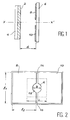
- Figure 1 shows the structure of a tunable Fabry-Pérot interferometer controlled electrostatically, according to the invention.
- This structure comprises a first fixed mirror 4, with which a floating electrode 2 is associated.
- the fixed mirror 4 is formed for example on a substrate.
- the floating electrode 2 is produced on the surface of the mirror 4.
- This mirror 4 consists of a stack of layers of different dielectrics (for example SiO 2 and Si undoped; or else at least one layer of SiO 2 and one layer of undoped Si, the undoped Si being a dielectric).
- the floating electrode may be the last layer of the stack forming the mirror, it then consists of doped silicon, therefore conductive.
- Facing the fixed mirror 2 is a second mirror 6, mobile, along an axis XX 'of the interferometer.
- Two second control electrodes 8, 10 are associated with this second mirror. These are for example produced by metallization of part of a reflecting membrane forming the second mirror 6.
- the two mirrors are held one relative to the other at a distance d. This distance is actually the length of the resonant cavity defined by the mirrors 4, 6.
- Keeping the two mirrors at a distance d is made using, for example, sleepers or stops, or spacers not shown in the figure 1.
- the cavity thus formed defines, from the electrical point of view, a capacitance C 1 between the control electrodes 8, 10 and the floating electrode 2.
- the application of an electric voltage between the control electrodes modifies, through the capacitance C 1 of the air gap, the potential of the floating electrode 2, and thus the movable mirror 6 is attracted towards the fixed mirror.
- control electrodes 8, 10 are made by metallic deposition on a surface, or membrane, reflective.
- the metallic deposit leaves a circular opening 12 on the surface reflective, thus leaving a central area free, reflective and mobile.
- the deposit leaves two free trenches 14, 16 used to isolate the electrodes of command 8, 10 relative to each other.
- the electrodes can be produced by metallic deposition then by etching of zones 12, 14, 16.
- FIG. 3 An embodiment of an interferometer according to the invention is illustrated in FIG. 3.
- This interferometer is produced in two substrates 20, 22, for example in silicon of SOI type ("Silicon On Insulator").
- Mirrors 32, 26 are produced by depositing thin layers: these are for example deposits made up of a stack of different dielectrics, for example SiO 2 and Si (the undoped Si is a dielectric), of thickness ⁇ / 4, alternating and produced on each of the faces 28, 30 of the two substrates intended to be opposite one another.
- the thickness and the number of layers of each stack to be deposited depends on the wavelength at which the filter, or the interferometer, is intended to resonate, as well as on the desired emission finesse.
- the outer layer 24 of the stack is formed of doped silicon to make it conductive.
- the two mirrors 32, 26 define a cavity Fabry-Pérot whose resonance wavelengths are defined by equation (1) above, the distance d being the distance between the surfaces of the two mirrors.
- the fixed mirror 32 is provided with an electrode, called floating, 24.
- the mirror 26 is provided with two electrodes 38, 40, for example having the form described above in conjunction with Figure 2. At these electrodes associated with electrical contacts. Two cavities 42, 44 etched in the substrate 22 possibly allow to leave a passage for these electrical contacts.
- the floating electrode can be produced by example by strong doping of the substrate 22.
- Maintaining the two substrates, one relative to the other, in the desired position so as to define a Fabry-Pérot cavity of length d, is provided by stops 46, 48 and by sealing with seals, or resin pads 50, 52.
- seals, or resin pads 50, 52 Preferably, we leave in the resin joints of the vents which allow equalize the pressures inside and outside the Fabry-Pérot cavity.
- FIG. 4 represents an electrical diagram equivalent to the overall structure, where C 1 denotes the control capacitance produced between the control electrode and the floating electrode, and where C 2 denotes the parasitic capacitance, due for example, in the mode of FIG. 2, in the trenches 14, 16. Still taking the example of FIG.
- This simulation was carried out using the finite element method (ANSYS).
- FIG. 5 illustrates the result: it represents only half of the membrane (mobile central zone 54 and metallized peripheral zone 56), the arrows representing the zone where the electrostatic force is applied.
- the deflection ⁇ obtained is 0.32 ⁇ m.
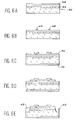
- FIGS. 6A to 6M represent stages of realization of a device according to the invention.
- FIGS. 6A to 6F represent the steps of realization of a first part of the interferometer.
- a substrate 60 for example of the SOI type, with a deposit 62 of SiO 2 on the front face.
- the reference 64 also designates an SiO 2 layer. Between the two is a layer 63 of Si.
- a photolithography step is then carried out: a positive resin is spread on the substrate ("schipley 1828" type resin), which is dried.
- An insolation step makes it possible to define the shape of the separation stops (FIG. 6B: stops 46, 48 of FIG. 3).
- Development is then carried out, that is to say the removal of the insolated resin, then annealing.
- the engraving of the stops can be performed at CHF 3 / O 2 and the removal of the resin with fuming nitric acid.
- the next step is a step of etching the Si 3 N 4 front face by photolithography of positive resin (to define the cavities 42, 44), etching with CHF 3 / O 2 and removal of the resin with HNO 3 smoking.
- the Si 3 N 4 is removed on the front panel by etching the CHF 3 / O 2 .
- Figures 6G to 6L show stages of realization of a second part of an interferometer.
- An opening 76 is made in the rear resin layer (FIG. 6J), by photolithography with positive resin, etching of the rear face of Si 3 N 4 at CHF 3 / O 2 and removal of the resin with fuming HNO 3 .
- the front layer 74 of Si 3 N 4 is etched at CHF 3 / O 2 in order to release the control electrodes.
- the floating electrode is associated to the moving mirror, this is the substrate on which this electrode is made which is etched, not the substrate on which the electrodes are made ordered.
- the interferometer according to the invention is tunable and can be integrated into any gas analysis system which requires a wavelength selection. His tunable nature makes it possible to detect several gases, depending on the wavelength of job. It is also possible to work in optical frequency modulation.
- the interferometer according to the invention can be used for telecommunications, because micro-machining of silicon allows very small cavities, and therefore resonances around the lengths wave at 1.3 ⁇ m and 1.55 ⁇ m.
Landscapes
- Physics & Mathematics (AREA)
- Spectroscopy & Molecular Physics (AREA)
- General Physics & Mathematics (AREA)
- Optics & Photonics (AREA)
- Mechanical Light Control Or Optical Switches (AREA)
- Spectrometry And Color Measurement (AREA)
- Micromachines (AREA)
Abstract
Description
L'invention concerne le domaine de l'interférométrie, et plus particulièrement la réalisation d'un interféromètre Fabry-Pérot, commandable électrostatiquement et accordable. Un tel dispositif est par exemple utilisé comme filtre interférométrique.The invention relates to the field of interferometry, and more particularly the production of a Fabry-Pérot interferometer, electrostatically controllable and tunable. Such device is for example used as a filter interferometric.
Les documents EP-668 490 et EP 693 683 décrivent des interféromètres Fabry-Pérot intégrés, à commande électrostatique.EP-668,490 and EP 693,683 describe integrated Fabry-Pérot interferometers, to order electrostatic.
On trouve également la description de tels interféromètres dans l'article de M. Blomberg et al., intitulé "Electrically Tunable Micromachined Fabry-Pérot Interferometer in Gas Analysis" paru dans Physica Scripta, vol. T69, pages 119-121, 1997 et dans l'article de M. Viitasalo et al., intitulé "Carbon Dioxide Sensor based on Micromachined Fabry-Pérot Interferometer" paru dans SENSOR 97, Poster A7.36, pages 193-198.There is also a description of such interferometers in the article by M. Blomberg et al., entitled "Electrically Tunable Micromachined Fabry-Pérot Interferometer in Gas Analysis "published in Physica Scripta, vol. T69, pages 119-121, 1997 and in the article by M. Viitasalo et al., entitled "Carbon Dioxide Sensor based on Micromachined Fabry-Pérot Interferometer "published in SENSOR 97, Poster A7.36, pages 193-198.
Dans ces documents, une cavité optique résonante est usinée dans un substrat de silicium. Cette cavité est une couche d'air d'épaisseur λ/2, λ étant la longueur d'onde de travail, qui est usinée entre deux miroirs diélectriques parallèles. L'un des miroirs est mobile, tandis que l'autre reste fixe. Chacun de ces miroirs porte des électrodes de commande, qui peuvent être réalisées sous la forme de dépôts conducteurs de couches de silicium fortement dopé. L'application d'une différence de potentiel entre ces électrodes de commande attire le miroir mobile vers le miroir fixe, modifiant ainsi l'épaisseur d'air, et donc la longueur d'onde de résonance.In these documents, a resonant optical cavity is machined in a silicon substrate. This cavity is an air layer of thickness λ / 2, λ being the working wavelength, which is machined between two parallel dielectric mirrors. One of the mirrors is mobile, while the other remains fixed. Each of these mirrors carries control electrodes, which can be produced in the form of conductive deposits of highly doped silicon layers. The application of a potential difference between these control electrodes attracts the movable mirror towards the fixed mirror, thus modifying the air thickness, and therefore the resonance wavelength.
Dans le document EP-668 490, l'électrode du miroir mobile est annulaire et le fait d'usiner une zone amincie sur le pourtour du miroir en rend le centre plus rigide, et améliore le déplacement plan de la zone optique utile centrale.In document EP-668 490, the electrode of the mirror mobile is annular and machining an area thinner around the mirror makes the center of it more rigid, and improves the plane displacement of the area useful central optics.
Les dispositifs décrits dans ces divers documents mettent en oeuvre des électrodes de commande portées par les deux miroirs parallèles. La commande électrostatique se fait directement par l'application d'une tension sur ces électrodes. Cette technique oblige à prendre des contacts électriques sur deux faces conductrices en regard, d'où une certaine complexité du dispositif résultant, et du procédé permettant de le réaliser. En particulier, la prise de contact sur le miroir supérieur est délicate, et nécessite un empilement local de couches fortement dopées. Une très grande attention doit donc être portée sur l'isolation des différentes parties actives, afin d'éviter tout court-circuit.The devices described in these various documents use mounted control electrodes by the two parallel mirrors. The command electrostatic is done directly by application of a voltage on these electrodes. This technique requires making electrical contacts out of two conductive faces opposite, hence a certain complexity of the resulting device, and of the process allowing to realize it. In particular, taking contact on the upper mirror is delicate, and requires local stacking of layers strongly doped. Very great attention must therefore be paid on the insulation of the different active parts, so avoid any short circuit.
La présente invention a pour objet un interféromètre Fabry-Pérot accordable, commandé électrostatiquement, comportant :
- un premier miroir, auquel est associé une électrode flottante,
- un second miroir, auquel sont associées une première et une seconde électrodes de commande, l'un des premier et second miroirs étant fixe tandis que l'autre est mobile,
- une cavité résonnante, de longueur d, délimitée par les premier et second miroirs, l'application d'une tension électrique entre les deux électrodes de commande entraínant un déplacement du miroir mobile par rapport au miroir fixe et modifiant donc la longueur d de la cavité résonante.
- a first mirror, with which a floating electrode is associated,
- a second mirror, with which are associated first and second control electrodes, one of the first and second mirrors being fixed while the other is mobile,
- a resonant cavity, of length d, delimited by the first and second mirrors, the application of an electric voltage between the two control electrodes causing the movable mirror to move relative to the fixed mirror and therefore modifying the length d of the cavity resonant.
Dans la mesure où l'électrode associée à l'un des miroirs est une électrode flottante, aucune prise de contact n'est à réaliser du côté de ce miroir. Il n'y a donc plus, dans le système final, qu'un seul niveau de contact à prendre, correspondant aux électrodes de commande.Insofar as the electrode associated with one of the mirrors is a floating electrode, no socket contact is not to be made on the side of this mirror. There is therefore more, in the final system, than a single level of contact to be made, corresponding to the electrodes of ordered.
Par conséquent, l'interféromètre selon l'invention est toujours à commande électrostatique, mais les deux électrodes de commande sont ramenées sur un seul côté du dispositif.Consequently, the interferometer according to the invention is still electrostatic, but both control electrodes are brought to one side of the device.
L'électrode flottante et le miroir auquel elle est associée peuvent être réalisés en surface d'un premier substrat. Par exemple, ce substrat est en silicium et l'électrode flottante est réalisée en silicium dopé.The floating electrode and the mirror to which it is associated can be made on the surface of a first substrate. For example, this substrate is made of silicon and the floating electrode is made of doped silicon.
L'autre miroir, et ses électrodes de commande peuvent être réalisés en surface d'un second substrat, par exemple, lui aussi, en silicium.The other mirror, and its control electrodes can be made on the surface of a second substrate, for example, too, made of silicon.
Selon un mode particulier de réalisation, le miroir mobile peut être constitué d'une membrane gravée dans un substrat.According to a particular embodiment, the mobile mirror can consist of an engraved membrane in a substrate.
Quant aux électrodes de commande, elles peuvent être formées de part et d'autre d'une zone réfléchissante à laquelle elles sont associées, par exemple le miroir mobile. En d'autres termes, ce miroir comporte une zone centrale réfléchissante et des zones latérales sur lesquelles sont déposées les électrodes de commande.As for the control electrodes, they can be formed on either side of an area reflective with which they are associated, by example the mobile mirror. In other words, this mirror has a reflective central zone and zones side on which the electrodes are placed control.
Cette zone centrale réfléchissante peut avoir une forme circulaire. Dans le cas où il s'agit du miroir mobile, cette forme circulaire, délimitée par les électrodes de commande, permet un déplacement parfaitement plan de la zone réfléchissante mobile, puisque l'attraction électrostatique n'a lieu qu'à la périphérie de cette zone, ce qui permet d'avoir une sortie de filtre diaphragmée.This central reflective area can have a circular shape. In case it is the mirror mobile, this circular shape, delimited by control electrodes, allows movement perfectly plan of the moving reflective area, since the electrostatic attraction only takes place at the periphery of this area, which allows to have a diaphragm filter outlet.
Les électrodes de commande peuvent être réalisées en un dépôt métallique. Par ailleurs, des contacts électriques peuvent être pris directement sur les électrodes de commande, en surface d'un des substrats.Control electrodes can be realized in a metallic deposit. In addition, contacts can be taken directly from the control electrodes, on the surface of one of the substrates.
L'invention a également pour objet un procédé de réalisation d'un interféromètre Fabry-Pérot accordable, comportant :
- une étape de réalisation d'un premier ensemble comportant un premier miroir et une électrode flottante associée à ce premier miroir,
- une étape de réalisation d'un second ensemble comportant un second miroir, présentant une zone réfléchissante, et une première et une seconde électrodes de commande associées à ce second miroir, l'un des miroirs étant fixe, tandis que l'autre est mobile,
- une étape de réalisation d'une cavité résonante, de longueur d, délimitée par les premier et second miroir, par assemblage des premier et second ensembles, l'application d'une tension électrique entre les électrodes de commande entraínant un déplacement de la zone réfléchissante du miroir mobile par rapport au miroir fixe et modifiant donc la longueur d de la cavité.
- a step of producing a first assembly comprising a first mirror and a floating electrode associated with this first mirror,
- a step of producing a second assembly comprising a second mirror, having a reflecting zone, and first and second control electrodes associated with this second mirror, one of the mirrors being fixed, while the other is mobile,
- a step of producing a resonant cavity, of length d, delimited by the first and second mirror, by assembling the first and second sets, the application of an electric voltage between the control electrodes causing a displacement of the reflective zone of the movable mirror relative to the fixed mirror and thus modifying the length d of the cavity.
En particulier, l'électrode flottante et le miroir correspondant peuvent être réalisés en surface d'un premier substrat. Par exemple, le substrat peut être en silicium et l'électrode flottante peut être réalisée par dopage d'une couche mince de silicium en surface du premier miroir formé d'au moins une couche diélectrique, premier miroir déposé lui-même sur le substrat. L'électrode flottante peut être aussi réalisée par un dépôt métallique disposé sur le miroir.In particular, the floating electrode and the mirror corresponding can be made on the surface of a first substrate. For example, the substrate can be in silicon and the floating electrode can be realized by doping a thin layer of silicon on the surface of the first mirror formed from at least one layer dielectric, first mirror deposited itself on the substrate. The floating electrode can also be produced by a metal deposit placed on the mirror.
L'autre miroir, ainsi que les première et seconde électrodes de commande peuvent être réalisées en surface d'un second substrat. Par exemple, ce second miroir est constitué d'une membrane dont une partie (la zone réfléchissante mobile) est rendue mobile par gravure du second substrat.The other mirror, as well as the first and second control electrodes can be made in surface of a second substrate. For example, this second mirror consists of a membrane, part of which (the mobile reflective zone) is made mobile by etching of the second substrate.
Les électrodes de commande, quant à elles, peuvent être réalisées par dépôt métallique sur l'un des miroirs.The control electrodes, on the other hand, can be made by metallic deposition on one of the mirrors.
- la figure 1 représente schématiquement un interféromètre Fabry-Pérot accordable, selon l'invention,Figure 1 schematically shows a tunable Fabry-Pérot interferometer, according to the invention,
- la figure 2 représente une vue de dessus des électrodes de commande et du miroir mobile dans un interféromètre selon l'invention,FIG. 2 represents a top view of the control electrodes and movable mirror in an interferometer according to the invention,
- la figure 3 est une vue en coupe d'un mode de réalisation d'un interféromètre selon l'invention, Figure 3 is a sectional view of a mode of production of an interferometer according to the invention,
- la figure 4 est un schéma électrique équivalent des électrodes de commande d'un interféromètre selon l'invention,Figure 4 is an equivalent electrical diagram control electrodes of an interferometer according to the invention,
- la figure 5 représente une simulation de la déflexion du membrane réfléchissante dans un interféromètre selon l'invention,Figure 5 shows a simulation of the deflection of the reflective membrane in a interferometer according to the invention,
- les figures 6A-6M représentent des étapes pour réalisation d'un interféromètre selon l'invention.Figures 6A-6M show steps for production of an interferometer according to the invention.
La figure 1 représente la structure d'un interféromètre Fabry-Pérot accordable commandé électrostatiquement, conforme à l'invention.Figure 1 shows the structure of a tunable Fabry-Pérot interferometer controlled electrostatically, according to the invention.
Cette structure comporte un premier miroir 4,
fixe, auquel est associée une électrode flottante 2. Le
miroir fixe 4 est formé par exemple sur un substrat.
L'électrode flottante 2 est réalisée à la surface du
miroir 4. Ce miroir 4 est constitué d'un empilement de
couches de diélectriques différents (par exemple SiO2
et Si non dopé ; ou bien au moins une couche de SiO2 et
une couche de Si non dopé, le Si non dopé étant un
diélectrique). L'électrode flottante peut être la
dernière couche de l'empilement formant le miroir, elle
est alors constituée de silicium dopé, donc conducteur.
Face au miroir fixe 2 se trouve un second miroir 6,
mobile, selon un axe XX' de l'interféromètre. A ce
second miroir sont associées deux électrodes de
commande 8, 10. Celles-ci sont par exemple réalisées
par métallisation d'une partie d'une membrane
réflectrice formant le second miroir 6.This structure comprises a first fixed mirror 4, with which a
Les deux miroirs sont maintenus l'un par rapport à
l'autre à une distance d. Cette distance est en fait la
longueur de la cavité résonante délimitée par les
miroirs 4, 6.The two mirrors are held one relative to
the other at a distance d. This distance is actually the
length of the resonant cavity defined by the
Le maintien des deux miroirs à une distance d est réalisé à l'aide, par exemple, de traverses ou de butées, ou d'entretoises non représentées sur la figure 1.Keeping the two mirrors at a distance d is made using, for example, sleepers or stops, or spacers not shown in the figure 1.
L'application d'une tension électrique, à l'aide
de moyens non représentés sur la figure 1, entre les
deux électrodes de commande 8, 10 entraíne un
déplacement du miroir mobile 6 par rapport au miroir
fixe, le long de l'axe XX', et modifie donc la longueur
de la cavité résonante.Applying an electrical voltage, using
means not shown in FIG. 1, between the
two
La longueur d de la cavité Fabry-Pérot satisfait à
la relation :
La cavité ainsi formée définit, du point de vue
électrique, une capacité C1 entre les électrodes de
commande 8, 10 et l'électrode flottante 2. En fait,
l'application d'une tension électrique entre les
électrodes de commande, modifie, à travers la capacité
C1 de l'entrefer, le potentiel de l'électrode flottante
2, et, ainsi, le miroir mobile 6 est attiré en
direction du miroir fixe.The cavity thus formed defines, from the electrical point of view, a capacitance C 1 between the
Le fonctionnement exposé ci-dessus n'est pas modifié si l'électrode flottante est associée au miroir mobile et les électrodes de commande au miroir fixe. On décrit ci-dessous, de manière détaillée, le cas où l'électrode flottante est associée au miroir fixe, mais l'enseignement de l'invention concerne les deux cas et le second cas peut être facilement réalisé à partir du premier en inversant les électrodes de commande et l'électrode de référence.The operation described above is not modified if the floating electrode is associated with the mirror mobile and the control electrodes to the fixed mirror. We described below, in detail, the case where the floating electrode is associated with the fixed mirror, but the teaching of the invention relates to both cases and the second case can be easily realized from the first by reversing the control electrodes and the reference electrode.
Une vue de dessus des électrodes de commande 8, 10
et du miroir mobile est donnée en figure 2 : selon ce
mode de réalisation, les électrodes de commande 8, 10
sont réalisées par dépôt métallique sur une surface, ou
membrane, réfléchissante. Le dépôt métallique laisse
une ouverture circulaire 12 sur la surface
réfléchissante, laissant ainsi libre une zone centrale,
réfléchissante et mobile. Le dépôt laisse libre deux
tranchées 14, 16 permettant d'isoler les électrodes de
commande 8, 10 l'une par rapport à l'autre.
Pratiquement, les électrodes peuvent être réalisées par
dépôt métallique puis par gravure des zones 12, 14, 16.A top view of the
Un mode de réalisation d'un interféromètre selon
l'invention est illustré en figure 3. Cet
interféromètre est réalisé dans deux substrats 20, 22,
par exemple en silicium de type SOI ("Silicon On
Insulator"). Des miroirs 32, 26 sont réalisés par dépôt
de couches minces : ce sont par exemple des dépôts
constitués d'un empilement de diélectriques différents,
par exemple de SiO2 et de Si (le Si non dopé est un
diélectrique), d'épaisseur λ/4, alternés et réalisés
sur chacune des faces 28, 30 des deux substrats
destinées à être en regard l'une de l'autre.
L'épaisseur et le nombre des couches de chaque
empilement à déposer dépend de la longueur d'onde à
laquelle le filtre, ou l'interféromètre, est destiné à
résonner, ainsi que de la finesse d'émission voulue. An embodiment of an interferometer according to the invention is illustrated in FIG. 3. This interferometer is produced in two
Sur le miroir 32, la couche externe 24 de
l'empilement est formée de silicium dopé pour la rendre
conductrice.On the
Les deux miroirs 32, 26 définissent une cavité Fabry-Pérot dont les longueurs d'onde de résonance sont définies par l'équation (1) ci-dessus, la distance d étant la distance séparant les surfaces des deux miroirs.The two mirrors 32, 26 define a cavity Fabry-Pérot whose resonance wavelengths are defined by equation (1) above, the distance d being the distance between the surfaces of the two mirrors.
Le miroir fixe 32 est muni d'une électrode, dite
flottante, 24. Le miroir 26 est muni de deux électrodes
de commande 38, 40, ayant par exemple la forme décrite
ci-dessus en liaison avec la figure 2. A ces électrodes
de commande sont associés des contacts électriques.
Deux cavités 42, 44 gravées dans le substrat 22
permettent éventuellement de laisser un passage pour
ces contacts électriques.The fixed
L'électrode flottante peut être réalisée par
exemple par un dopage fort du substrat 22.The floating electrode can be produced by
example by strong doping of the
Le maintien des deux substrats, l'un par rapport à
l'autre, dans la position voulue de manière à définir
une cavité Fabry-Pérot de longueur d, est assuré par
des butées 46, 48 et par scellement à l'aide de joints,
ou de plots en résine 50, 52. De préférence, on laisse
dans les joints en résine des évents qui permettent de
réaliser une égalisation des pressions à l'intérieur et
à l'extérieur de la cavité Fabry-Pérot.Maintaining the two substrates, one relative to
the other, in the desired position so as to define
a Fabry-Pérot cavity of length d, is provided by
La figure 4 représente un schéma électrique
équivalent à la structure globale, ou C1 désigne la
capacité de commande réalisée entre l'électrode de
commande et l'électrode flottante, et où C2 désigne la
capacité parasite, due par exemple, dans le mode de
réalisation de la figure 2, aux tranchées 14, 16.
Toujours en prenant l'exemple de la figure 2, avec un
diamètre D=1 mm et une longueur L=1,37 mm (distance
entre les deux plots 46, 48), des électrodes de taille
l1=2 mm et l2=1,9 mm, des tranchées 14, 16 de largeur
égale à environ 10 µm, des électrodes 8, 10 réalisées
par un dépôt métallique d'épaisseur égal à environ
300 nm, on obtient, pour une distance d=1,8 µm :
Une simulation de la déflexion d'un miroir mobile,
ayant la forme d'une membrane constituée d'un
empilement de couches Si3N4 (épaisseur : 2 µm) /SiO2
(épaisseur : 0,7 µm)/Si (épaisseur : 0,3 µm)/SiO2
(épaisseur : 0,7 µm)/Si (épaisseur : 0,3 µm), sous une
tension de 30 volts a permis de vérifier que la
déflexion est plane sur toute la partie centrale active
de la membrane. Dans cet exemple, la tension est
appliquée entre deux électrodes parallèles. Cette
simulation a été réalisée grâce à la méthode des
éléments finis (ANSYS). La figure 5 illustre le
résultat : elle ne représente qu'une moitié de la
membrane (zone centrale mobile 54 et zone périphérique
métallisée 56), les flèches représentant la zone où la
force électrostatique est appliquée. La déflexion δ
obtenue est de 0,32 µm.A simulation of the deflection of a mobile mirror, in the form of a membrane consisting of a stack of layers Si 3 N 4 (thickness: 2 µm) / SiO 2 (thickness: 0.7 µm) / Si (thickness : 0.3 µm) / SiO 2 (thickness: 0.7 µm) / Si (thickness: 0.3 µm), at a voltage of 30 volts verified that the deflection is flat over the entire active central part of the membrane. In this example, voltage is applied between two parallel electrodes. This simulation was carried out using the finite element method (ANSYS). FIG. 5 illustrates the result: it represents only half of the membrane (mobile
Les figures 6A à 6M représentent des étapes de réalisation d'un dispositif selon l'invention.FIGS. 6A to 6M represent stages of realization of a device according to the invention.
Les figures 6A à 6F représentent les étapes de réalisation d'une première partie de l'interféromètre.FIGS. 6A to 6F represent the steps of realization of a first part of the interferometer.
Tout d'abord, on considère un substrat 60, par
exemple de type SOI, avec un dépôt 62 de SiO2 en face
avant. La référence 64 désigne également une couche
SiO2. Entre les deux se trouve une couche 63 de Si. First of all, we consider a
On réalise ensuite une étape de photolithographie : on étale une résine positive sur le substrat (résine de type "schipley 1828"), que l'on sèche. Une étape d'insolation permet de définir la forme des butées de séparation (figure 6B : butées 46, 48 de la figure 3) . On réalise ensuite le développement, c'est-à-dire le retrait de la résine insolée, puis un recuit. La gravure des butées peut être réalisée au CHF3/O2 et le retrait de la résine avec de l'acide nitrique fumant.A photolithography step is then carried out: a positive resin is spread on the substrate ("schipley 1828" type resin), which is dried. An insolation step makes it possible to define the shape of the separation stops (FIG. 6B: stops 46, 48 of FIG. 3). Development is then carried out, that is to say the removal of the insolated resin, then annealing. The engraving of the stops can be performed at CHF 3 / O 2 and the removal of the resin with fuming nitric acid.
On réalise ensuite sur les butées obtenues (figure
6C) un dépôt 70 de Si3N4 (d'épaisseur 1 µm) double face.Then carried out on the stops obtained (Figure 6C) a
L'étape suivante (figure 6D) est une étape de
gravure face avant du Si3N4 par photolithographie de
résine positive (pour définir les cavités 42, 44), de
gravure au CHF3/O2 et de retrait de la résine au HNO3
fumant.The next step (FIG. 6D) is a step of etching the Si 3 N 4 front face by photolithography of positive resin (to define the
Ensuite (figure 6E) on réalise la gravure des
cavités 42, 44 au CHF3/O2, puis au KOH à 20% et 85°C,
pendant environ 2 heures.Then (FIG. 6E) the
Enfin (figure 6F), on retire le Si3N4 en face avant par gravure du CHF3/O2.Finally (FIG. 6F), the Si 3 N 4 is removed on the front panel by etching the CHF 3 / O 2 .
Les figures 6G à 6L représentent des étapes de réalisation d'une deuxième partie d'un interféromètre.Figures 6G to 6L show stages of realization of a second part of an interferometer.
On considère, là aussi, un substrat de départ 72
de type SOI, sur lequel on réalise un dépôt 74 de
chrome (10 nm d'épaisseur) et d'or (300 nm d'épaisseur)
en face avant.Here again, we consider a starting
Puis, (figure 6H), on réalise la gravure des électrodes de commande par :
- photolithographie par résine positive,
- gravure de la couche d'or (à l'aide d'un mélange de 80 g de NH4I, 20 g de I2 dans 400 ml de H2O et 600 ml d'éthanol),
- gravure de la couche de chrome (par mélange de 25 g de Ce(SO4)2, 2NH2SO4, 2H2O dans 625 ml de H2O et 125 ml de HNO3),
- retrait de la résine au HNO3 fumant.
- photolithography by positive resin,
- etching of the gold layer (using a mixture of 80 g of NH 4 I, 20 g of I 2 in 400 ml of H 2 O and 600 ml of ethanol),
- etching of the chromium layer (by mixing 25 g of Ce (SO 4 ) 2 , 2NH 2 SO 4 , 2H 2 O in 625 ml of H 2 O and 125 ml of HNO 3 ),
- removal of the resin with fuming HNO 3 .
Ensuite, (figure 6I), on réalise un dépôt 74 de
Si3N4 d'épaisseur 1 µm, en double face.Then, (FIG. 6I), a
Une ouverture 76 est réalisée dans la couche
arrière de résine (figure 6J), par photolithographie
par résine positive, gravure de la face arrière de Si3N4
au CHF3/O2 et retrait de la résine au HNO3 fumant.An
L'étape suivante (figure 6K) permet de graver la
face arrière de la membrane réfléchissante au KOH à 20%
(85°C pendant 5 heures). On réalise ainsi la cavité 80.The next step (Figure 6K) allows you to burn the
back of the 20% KOH reflective membrane
(85 ° C for 5 hours). The
La couche avant 74 de Si3N4 est gravée au CHF3/O2
afin de libérer les électrodes de commande.The
Puis, (figure 6M), les deux structures ainsi
obtenues sont mises en contact et scellées par résine
négative. On réalise une photolithographie de résine
négative sur la face avant du substrat 60 et le
scellement est effectué à 200°C.Then, (figure 6M), the two structures thus
obtained are brought into contact and sealed with resin
negative. We carry out a photolithography of resin
negative on the front face of
Enfin, une étape de prise de contact sur les électrodes de commande est réalisée.Finally, a step of making contact on the control electrodes is performed.
Dans le cas où l'électrode flottante est associée au miroir mobile, c'est le substrat sur lequel cette électrode est réalisée qui est gravé, et non pas le substrat sur lequel sont réalisées les électrodes de commande.In the case where the floating electrode is associated to the moving mirror, this is the substrate on which this electrode is made which is etched, not the substrate on which the electrodes are made ordered.
L'interféromètre selon l'invention est accordable et peut être intégré dans tout système d'analyse de gaz qui nécessite une sélection de longueur d'onde. Son caractère accordable rend possible une détection de plusieurs gaz, en fonction de la longueur d'onde de travail. Il est possible, également, de travailler en modulation de fréquence optique.The interferometer according to the invention is tunable and can be integrated into any gas analysis system which requires a wavelength selection. His tunable nature makes it possible to detect several gases, depending on the wavelength of job. It is also possible to work in optical frequency modulation.
Enfin, l'interféromètre selon l'invention peut être utilisé pour les télécommunications, car le micro-usinage de silicium permet de réaliser de très petites cavités, et donc des résonances autour des longueurs d'onde à 1,3 µm et 1,55 µm.Finally, the interferometer according to the invention can be used for telecommunications, because micro-machining of silicon allows very small cavities, and therefore resonances around the lengths wave at 1.3 µm and 1.55 µm.
Claims (22)
Applications Claiming Priority (2)
| Application Number | Priority Date | Filing Date | Title |
|---|---|---|---|
| FR9711696A FR2768812B1 (en) | 1997-09-19 | 1997-09-19 | FABRY-PEROT INTERFEROMETER TUNABLE INTEGRATED |
| FR9711696 | 1997-09-19 |
Publications (2)
| Publication Number | Publication Date |
|---|---|
| EP0903565A1 true EP0903565A1 (en) | 1999-03-24 |
| EP0903565B1 EP0903565B1 (en) | 2004-06-02 |
Family
ID=9511271
Family Applications (1)
| Application Number | Title | Priority Date | Filing Date |
|---|---|---|---|
| EP98402302A Expired - Lifetime EP0903565B1 (en) | 1997-09-19 | 1998-09-17 | Integrated tunable Fabry-Pérot interferometer |
Country Status (5)
| Country | Link |
|---|---|
| US (1) | US6078395A (en) |
| EP (1) | EP0903565B1 (en) |
| JP (1) | JP4578587B2 (en) |
| DE (1) | DE69824249T2 (en) |
| FR (1) | FR2768812B1 (en) |
Cited By (1)
| Publication number | Priority date | Publication date | Assignee | Title |
|---|---|---|---|---|
| WO2001059415A1 (en) * | 2000-02-14 | 2001-08-16 | Schlumberger Industries, S.A. | Short fabry-perot filter with metallic layers |
Families Citing this family (50)
| Publication number | Priority date | Publication date | Assignee | Title |
|---|---|---|---|---|
| FI981456A0 (en) * | 1998-06-24 | 1998-06-24 | Valtion Teknillinen | Method for electrically controlling the distance between micromechanical electrodes |
| US6295130B1 (en) * | 1999-12-22 | 2001-09-25 | Xerox Corporation | Structure and method for a microelectromechanically tunable fabry-perot cavity spectrophotometer |
| US6608711B2 (en) * | 2000-03-03 | 2003-08-19 | Axsun Technologies, Inc. | Silicon on insulator optical membrane structure for fabry-perot MOEMS filter |
| US6341039B1 (en) | 2000-03-03 | 2002-01-22 | Axsun Technologies, Inc. | Flexible membrane for tunable fabry-perot filter |
| US6836366B1 (en) | 2000-03-03 | 2004-12-28 | Axsun Technologies, Inc. | Integrated tunable fabry-perot filter and method of making same |
| US6373632B1 (en) | 2000-03-03 | 2002-04-16 | Axsun Technologies, Inc. | Tunable Fabry-Perot filter |
| US6597461B1 (en) | 2000-03-20 | 2003-07-22 | Parvenu, Inc. | Tunable fabry-perot interferometer using entropic materials |
| US6665109B2 (en) | 2000-03-20 | 2003-12-16 | Np Photonics, Inc. | Compliant mechanism and method of forming same |
| US6747775B2 (en) * | 2000-03-20 | 2004-06-08 | Np Photonics, Inc. | Detunable Fabry-Perot interferometer and an add/drop multiplexer using the same |
| US6678084B2 (en) | 2000-03-20 | 2004-01-13 | Np Photonics, Inc. | Methods of making mechanisms in which relative locations of elements are maintained during manufacturing |
| AU2001249289A1 (en) | 2000-03-20 | 2001-10-03 | Solus Micro Technologies, Inc. | Electrostatically-actuated tunable optical components using entropic materials |
| US6747784B2 (en) | 2000-03-20 | 2004-06-08 | Np Photonics, Inc. | Compliant mechanism and method of forming same |
| US6356689B1 (en) * | 2000-03-25 | 2002-03-12 | Lucent Technologies, Inc. | Article comprising an optical cavity |
| US6538748B1 (en) * | 2000-04-14 | 2003-03-25 | Agilent Technologies, Inc | Tunable Fabry-Perot filters and lasers utilizing feedback to reduce frequency noise |
| US6400738B1 (en) * | 2000-04-14 | 2002-06-04 | Agilent Technologies, Inc. | Tunable Fabry-Perot filters and lasers |
| US6721098B2 (en) | 2000-12-22 | 2004-04-13 | Axsun Technologies, Inc. | Triple electrode MOEMS tunable filter and fabrication process therefor |
| US7425453B1 (en) * | 2001-03-14 | 2008-09-16 | The United States Of America As Represented By The Secretary Of The Navy | Integrated circuit porphyrin-based optical Fabry-Perot chemical sensor |
| JP4720022B2 (en) * | 2001-05-30 | 2011-07-13 | ソニー株式会社 | OPTICAL MULTILAYER STRUCTURE, ITS MANUFACTURING METHOD, OPTICAL SWITCHING DEVICE, AND IMAGE DISPLAY DEVICE |
| KR100411328B1 (en) * | 2001-12-21 | 2003-12-18 | 한국과학기술원 | Tunable optical filter |
| KR100453975B1 (en) * | 2002-10-25 | 2004-10-20 | 전자부품연구원 | Micro Fabry-Perot filter driven by magnetic force and gas analysis apparatus using the same |
| US6996312B2 (en) * | 2003-04-29 | 2006-02-07 | Rosemount, Inc. | Tunable fabry-perot filter |
| JP4166712B2 (en) * | 2004-01-29 | 2008-10-15 | 株式会社デンソー | Fabry-Perot filter |
| US7061660B1 (en) * | 2005-04-13 | 2006-06-13 | Hewlett-Packard Development Company, L.P. | MEMs device with feedback control |
| US7804600B1 (en) | 2007-04-30 | 2010-09-28 | The United States Of America As Represented By The Administrator Of The National Aeronautics And Space Administration | Ring-laser gyroscope system using dispersive element(s) |
| US8174698B2 (en) * | 2007-08-10 | 2012-05-08 | Corporation de l'Ecole Polytechnique de Montréal | MEMS tunable silicon fabry-perot cavity and applications thereof |
| FI125817B (en) * | 2009-01-27 | 2016-02-29 | Teknologian Tutkimuskeskus Vtt Oy | Improved electronically controlled Fabry-Perot interferometer, an intermediate product, an electrode system and a method for producing an electronically controlled Fabry-Perot interferometer |
| FI20095976A0 (en) * | 2009-09-24 | 2009-09-24 | Valtion Teknillinen | Micromechanically adjustable Fabry-Perot interferometer and method for its production |
| US8711361B2 (en) * | 2009-11-05 | 2014-04-29 | Qualcomm, Incorporated | Methods and devices for detecting and measuring environmental conditions in high performance device packages |
| JP5673075B2 (en) * | 2010-12-21 | 2015-02-18 | セイコーエプソン株式会社 | Tunable interference filter, optical module, and optical analyzer |
| JP5884393B2 (en) * | 2011-10-13 | 2016-03-15 | セイコーエプソン株式会社 | Wavelength variable interference filter, optical filter device, optical module, and electronic apparatus |
| US20120154915A1 (en) * | 2010-12-21 | 2012-06-21 | Seiko Epson Corporation | Variable wavelength interference filter, optical filter device, optical module, and electronic apparatus |
| JP2012150353A (en) * | 2011-01-20 | 2012-08-09 | Seiko Epson Corp | Wavelength variable interference filter, optical module, and optical analysis device |
| JP5724557B2 (en) | 2011-04-07 | 2015-05-27 | セイコーエプソン株式会社 | Tunable interference filter, optical module, and optical analyzer |
| JP6186692B2 (en) * | 2012-10-01 | 2017-08-30 | セイコーエプソン株式会社 | Wavelength variable interference filter, optical filter device, optical module, and electronic apparatus |
| US20140267443A1 (en) * | 2013-03-14 | 2014-09-18 | Qualcomm Mems Technologies, Inc. | Electromechanical systems device with segmented electrodes |
| US10613200B2 (en) | 2017-09-19 | 2020-04-07 | Veoneer, Inc. | Scanning lidar system and method |
| US11460550B2 (en) | 2017-09-19 | 2022-10-04 | Veoneer Us, Llc | Direct detection LiDAR system and method with synthetic doppler processing |
| US11194022B2 (en) | 2017-09-29 | 2021-12-07 | Veoneer Us, Inc. | Detection system with reflection member and offset detection array |
| US20190107622A1 (en) * | 2017-10-11 | 2019-04-11 | Veoneer Us, Inc. | Scanning LiDAR System and Method with Source Laser Beam Splitting Apparatus and Method |
| US11585901B2 (en) | 2017-11-15 | 2023-02-21 | Veoneer Us, Llc | Scanning lidar system and method with spatial filtering for reduction of ambient light |
| US11579257B2 (en) | 2019-07-15 | 2023-02-14 | Veoneer Us, Llc | Scanning LiDAR system and method with unitary optical element |
| US11474218B2 (en) | 2019-07-15 | 2022-10-18 | Veoneer Us, Llc | Scanning LiDAR system and method with unitary optical element |
| US11313969B2 (en) | 2019-10-28 | 2022-04-26 | Veoneer Us, Inc. | LiDAR homodyne transceiver using pulse-position modulation |
| US12044800B2 (en) | 2021-01-14 | 2024-07-23 | Magna Electronics, Llc | Scanning LiDAR system and method with compensation for transmit laser pulse effects |
| US11326758B1 (en) | 2021-03-12 | 2022-05-10 | Veoneer Us, Inc. | Spotlight illumination system using optical element |
| US11732858B2 (en) | 2021-06-18 | 2023-08-22 | Veoneer Us, Llc | Headlight illumination system using optical element |
| US12092278B2 (en) | 2022-10-07 | 2024-09-17 | Magna Electronics, Llc | Generating a spotlight |
| US12228653B2 (en) | 2022-10-07 | 2025-02-18 | Magna Electronics, Llc | Integrating a sensing system into headlight optics |
| US12202396B1 (en) | 2023-12-19 | 2025-01-21 | Magna Electronics, Llc | Line-scan-gated imaging for LiDAR headlight |
| WO2025227195A1 (en) * | 2024-05-01 | 2025-11-06 | The University Of Western Australia | Mems devices and methods of using and manufacturing mems devices |
Citations (2)
| Publication number | Priority date | Publication date | Assignee | Title |
|---|---|---|---|---|
| EP0219359A1 (en) * | 1985-10-16 | 1987-04-22 | BRITISH TELECOMMUNICATIONS public limited company | Fabry-perot interferometer |
| EP0668490A2 (en) * | 1994-02-17 | 1995-08-23 | Vaisala Oy | Electrically tunable fabry-perot interferometer produced by surface micromechanical techniques for use in optical material analysis |
Family Cites Families (7)
| Publication number | Priority date | Publication date | Assignee | Title |
|---|---|---|---|---|
| EP0046873A1 (en) * | 1980-09-02 | 1982-03-10 | Texas Instruments Incorporated | Deformable mirror light modulator |
| JPS62257032A (en) * | 1986-04-30 | 1987-11-09 | Sharp Corp | Variable interference apparatus |
| US4859060A (en) * | 1985-11-26 | 1989-08-22 | 501 Sharp Kabushiki Kaisha | Variable interferometric device and a process for the production of the same |
| US5909280A (en) * | 1992-01-22 | 1999-06-01 | Maxam, Inc. | Method of monolithically fabricating a microspectrometer with integrated detector |
| FI96450C (en) * | 1993-01-13 | 1996-06-25 | Vaisala Oy | Single-channel gas concentration measurement method and equipment |
| JP2555922B2 (en) * | 1993-02-26 | 1996-11-20 | 日本電気株式会社 | Electrostatically driven micro shutters and shutter arrays |
| FI98325C (en) * | 1994-07-07 | 1997-05-26 | Vaisala Oy | Selective infrared detector |
-
1997
- 1997-09-19 FR FR9711696A patent/FR2768812B1/en not_active Expired - Fee Related
-
1998
- 1998-09-02 US US09/145,261 patent/US6078395A/en not_active Expired - Lifetime
- 1998-09-16 JP JP26209798A patent/JP4578587B2/en not_active Expired - Fee Related
- 1998-09-17 DE DE69824249T patent/DE69824249T2/en not_active Expired - Lifetime
- 1998-09-17 EP EP98402302A patent/EP0903565B1/en not_active Expired - Lifetime
Patent Citations (2)
| Publication number | Priority date | Publication date | Assignee | Title |
|---|---|---|---|---|
| EP0219359A1 (en) * | 1985-10-16 | 1987-04-22 | BRITISH TELECOMMUNICATIONS public limited company | Fabry-perot interferometer |
| EP0668490A2 (en) * | 1994-02-17 | 1995-08-23 | Vaisala Oy | Electrically tunable fabry-perot interferometer produced by surface micromechanical techniques for use in optical material analysis |
Cited By (2)
| Publication number | Priority date | Publication date | Assignee | Title |
|---|---|---|---|---|
| WO2001059415A1 (en) * | 2000-02-14 | 2001-08-16 | Schlumberger Industries, S.A. | Short fabry-perot filter with metallic layers |
| FR2805052A1 (en) * | 2000-02-14 | 2001-08-17 | Schlumberger Ind Sa | FABRY-PEROT FILTER WITH METALLIC LAYERS |
Also Published As
| Publication number | Publication date |
|---|---|
| JP4578587B2 (en) | 2010-11-10 |
| JPH11167076A (en) | 1999-06-22 |
| DE69824249T2 (en) | 2005-07-14 |
| US6078395A (en) | 2000-06-20 |
| EP0903565B1 (en) | 2004-06-02 |
| FR2768812B1 (en) | 1999-10-22 |
| DE69824249D1 (en) | 2004-07-08 |
| FR2768812A1 (en) | 1999-03-26 |
Similar Documents
| Publication | Publication Date | Title |
|---|---|---|
| EP0903565B1 (en) | Integrated tunable Fabry-Pérot interferometer | |
| EP1364190B1 (en) | Optoelectronic device with wavelength filtering by cavity coupling | |
| US6466354B1 (en) | Method and apparatus for interferometric modulation of light | |
| US6519073B1 (en) | Micromechanical modulator and methods for fabricating the same | |
| US6813059B2 (en) | Reduced formation of asperities in contact micro-structures | |
| US5914804A (en) | Double-cavity micromechanical optical modulator with plural multilayer mirrors | |
| FR2768813A1 (en) | Miniaturized photo-acoustic spectrometer | |
| US20070242920A1 (en) | Fabry-Perot tunable filter using a bonded pair of transparent substrates | |
| FR2820834A1 (en) | METHOD FOR MANUFACTURING AN OPTICAL MICRO-MIRROR AND MICRO-MIRROR OR MICRO-MIRROR MATRIX OBTAINED BY THIS PROCESS | |
| US20090040616A1 (en) | Fabry-perot piezoelectric tunable filter | |
| CA2394108A1 (en) | Procedure for manufacturing a microelectromechanical optical component | |
| EP3257808A1 (en) | Microelectromechanical and/or nanoelectromechanical device with out-of-plane movement having capacitive means with surface variation | |
| EP1259847B1 (en) | Semiconductor optoelectronic device with electrically adjustable transfer function | |
| WO2010000824A1 (en) | Micro/nanostructured optical waveguiding structure for monitoring birefringence | |
| FR2820833A1 (en) | PIVOT OPTICAL MICRO-MIRROR, MATRIX OF SUCH MICRO-MIRRORS AND METHOD FOR PRODUCING SAID MICRO-MIRROR | |
| JP2005031326A (en) | Light filter | |
| CN104330890B (en) | Long-cavity-length micro-electromechanical tunable Fabry-Perot filter | |
| US20100315647A1 (en) | System, Method and Apparatus for a Micromachined Interferometer Using Optical Splitting | |
| FR2737019A1 (en) | SCANNING MICROELEMENTS FOR OPTICAL SYSTEM | |
| FR2865201A1 (en) | Vertical comb-drive type electrostatic actuator for very large telescope, has two electrode sets moving with respect to each other, from rest to maximum positions, where sets partially and electrically overlap even in rest position | |
| EP0876594B1 (en) | Tunable fabry-perot filter for determining gas concentration | |
| WO2001031755A1 (en) | Tuneable active microcavity and related method for making same | |
| JP2004205726A (en) | Beam splitter | |
| FR2949856A1 (en) | INTERFEROMETER WITH FIELD COMPENSATION | |
| FR2864634A1 (en) | Production of a mechanical driving system for an optical component, notably for adaptive optical components and micro-mirrors |
Legal Events
| Date | Code | Title | Description |
|---|---|---|---|
| PUAI | Public reference made under article 153(3) epc to a published international application that has entered the european phase |
Free format text: ORIGINAL CODE: 0009012 |
|
| AK | Designated contracting states |
Kind code of ref document: A1 Designated state(s): DE GB IT |
|
| AX | Request for extension of the european patent |
Free format text: AL;LT;LV;MK;RO;SI |
|
| 17P | Request for examination filed |
Effective date: 19990908 |
|
| AKX | Designation fees paid |
Free format text: DE GB IT |
|
| 17Q | First examination report despatched |
Effective date: 20030217 |
|
| GRAP | Despatch of communication of intention to grant a patent |
Free format text: ORIGINAL CODE: EPIDOSNIGR1 |
|
| GRAS | Grant fee paid |
Free format text: ORIGINAL CODE: EPIDOSNIGR3 |
|
| GRAA | (expected) grant |
Free format text: ORIGINAL CODE: 0009210 |
|
| AK | Designated contracting states |
Kind code of ref document: B1 Designated state(s): DE GB IT |
|
| REG | Reference to a national code |
Ref country code: GB Ref legal event code: FG4D Free format text: NOT ENGLISH |
|
| REF | Corresponds to: |
Ref document number: 69824249 Country of ref document: DE Date of ref document: 20040708 Kind code of ref document: P |
|
| GBT | Gb: translation of ep patent filed (gb section 77(6)(a)/1977) |
Effective date: 20040825 |
|
| PLBE | No opposition filed within time limit |
Free format text: ORIGINAL CODE: 0009261 |
|
| STAA | Information on the status of an ep patent application or granted ep patent |
Free format text: STATUS: NO OPPOSITION FILED WITHIN TIME LIMIT |
|
| 26N | No opposition filed |
Effective date: 20050303 |
|
| PGFP | Annual fee paid to national office [announced via postgrant information from national office to epo] |
Ref country code: GB Payment date: 20120918 Year of fee payment: 15 |
|
| PGFP | Annual fee paid to national office [announced via postgrant information from national office to epo] |
Ref country code: DE Payment date: 20120913 Year of fee payment: 15 Ref country code: IT Payment date: 20120924 Year of fee payment: 15 |
|
| GBPC | Gb: european patent ceased through non-payment of renewal fee |
Effective date: 20130917 |
|
| REG | Reference to a national code |
Ref country code: DE Ref legal event code: R119 Ref document number: 69824249 Country of ref document: DE Effective date: 20140401 |
|
| PG25 | Lapsed in a contracting state [announced via postgrant information from national office to epo] |
Ref country code: GB Free format text: LAPSE BECAUSE OF NON-PAYMENT OF DUE FEES Effective date: 20130917 |
|
| PG25 | Lapsed in a contracting state [announced via postgrant information from national office to epo] |
Ref country code: IT Free format text: LAPSE BECAUSE OF NON-PAYMENT OF DUE FEES Effective date: 20130917 Ref country code: DE Free format text: LAPSE BECAUSE OF NON-PAYMENT OF DUE FEES Effective date: 20140401 |